EP0255172A2 - Schaltkreis mit Hysterese - Google Patents
Schaltkreis mit Hysterese Download PDFInfo
- Publication number
- EP0255172A2 EP0255172A2 EP87201387A EP87201387A EP0255172A2 EP 0255172 A2 EP0255172 A2 EP 0255172A2 EP 87201387 A EP87201387 A EP 87201387A EP 87201387 A EP87201387 A EP 87201387A EP 0255172 A2 EP0255172 A2 EP 0255172A2
- Authority
- EP
- European Patent Office
- Prior art keywords
- circuit
- differential
- voltage
- hysteresis
- electrodes
- Prior art date
- Legal status (The legal status is an assumption and is not a legal conclusion. Google has not performed a legal analysis and makes no representation as to the accuracy of the status listed.)
- Granted
Links
Images

Classifications
-
- H—ELECTRICITY
- H03—ELECTRONIC CIRCUITRY
- H03K—PULSE TECHNIQUE
- H03K17/00—Electronic switching or gating, i.e. not by contact-making and –breaking
- H03K17/51—Electronic switching or gating, i.e. not by contact-making and –breaking characterised by the components used
- H03K17/56—Electronic switching or gating, i.e. not by contact-making and –breaking characterised by the components used by the use, as active elements, of semiconductor devices
- H03K17/687—Electronic switching or gating, i.e. not by contact-making and –breaking characterised by the components used by the use, as active elements, of semiconductor devices the devices being field-effect transistors
-
- H—ELECTRICITY
- H03—ELECTRONIC CIRCUITRY
- H03K—PULSE TECHNIQUE
- H03K3/00—Circuits for generating electric pulses; Monostable, bistable or multistable circuits
- H03K3/02—Generators characterised by the type of circuit or by the means used for producing pulses
- H03K3/353—Generators characterised by the type of circuit or by the means used for producing pulses by the use, as active elements, of field-effect transistors with internal or external positive feedback
- H03K3/356—Bistable circuits
- H03K3/3565—Bistables with hysteresis, e.g. Schmitt trigger
Definitions
- the invention relates to semiconductor switching circuits that exhibit hysteresis in which
- Switching circuits typically employ hysteresis to provide noise immunity or a safety margin.
- U.S. Patent 3,725,673 discloses a hysteresis circuit.
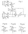
- Fig. 1 illustrates the basic features of this bipolar circuit. It switches between a pair of states with a hysteresis created by suitably switching a current I H .
- the circuit of Fig. 1 employs differential portions 11 and 12.
- Portion 11 amplifies an input vobage V I , which is here the amount by which a signal voltage V IN exceeds a reference voltage V REF , to produce circuit currents I1A and I 1B whose difference is representative of V I .
- the internal configuration (notshown) of portion 11 centers around a pair of Darlington circuits. Each Darlington contains an input PNP transistor whose emitter drives the base of a trailing PNP transistor. The bases of the input transistors differentially receive voltage V I .
- Currents I 1A and I 1B are respectively supplied from the collectors of the trailing transistors whose emitters are connected to a current source to receive a supply current.
- Portion 12 which is configured the same as portion 11, amplifies a control voltage V o to produce circuit currents I 2A and 1 2B whose difference is representative of V C .
- switch 15 is positioned at the high m value to set the circuit at the high threshold.
- V I the circuit changes state as V I rises above the high threshold.
- the new V o value causes switch 15 to switch to the lower m value. This sets the circuit at the low threshold.
- V I later drops nothing happens until it passes the low threshold. At that point, the circuit goes back to its original state. Switch 15 thereby returns to the high m value to reset the circuit at the high threshold.
- the circuit of U.S. Patent 3,725,673 has several desirable features.
- the amount of hysteresis can be controlled by simply adjusting K G or V C . Since K G is a ratio, it is largely independent of temperature and fabrication conditions. V c can be made largely temperature and process independent. Consequently, the hysteresis thresholds are stable with temperature and processing parameters.
- the flexibility is, howeer, somewhat limited because the, thresholds are not independently controllable. One of them is either fixed at zero (Figs. 2a and 2b) or is the negative of the other (Fig. 2c). It would be desirable to overcome this flexibility limitation without sacrificing the preceding advantages.
- a circuit switches between a pair of states with a hysteresis defined by separately controllable thresholds which can be made largely independent of temperature and fabrication parameters.
- the hysteresis is introduced into the circuit by using positive feedback to change the transconductance of a part of the circuit as it switches.
- the present circuit contains first and second differential portions.
- the first portion amplifies an input voltage to produce a pair of circuit currents whose difference is representative of the input voltage.
- the second portion amplifies a control voltage to produce another pair of circuit currents whose difference is representative of the control voltage.
- the four currents are operated on to causethe circuit to make state transitions as a function of the input voltage with a hysteresis whose magnitude depends on the control voltage. This is done with an arithmetic component and feedback circuitry.
- the arithmetic component produces a component signal at a value that varies largely in proportion to a linear combination of (1) the difference between the circuit currents of the first portion and (2) the difference between the circuit currents of the second portion. Generation of the component signal in this way establishes a switching region.
- the circuit makes transitions between its states largely in synchronism with transitions of the component signal.
- the feedback circuitry then creates the hysteresis by adjusting the transconductance of the second differential portion in response to the circuit transistions.
- the hysteresis consists of (1) a transition of a first type in which the circuit switches from one of its states to the other as the input voltage rises above a high threshold and (2) a transition of a second type opposite to the first as the input voltage drops below a low threshold less than the high threshold.
- the feedback circuitry decreases the transconductance of the second portion in response to a transition of the first type and vice versa.
- the primary element in the feedback circuitry is a switch that selectively decouples a part of a current source in the second portion from a pair of like-configured three-electrode amplifiers that are arranged in a differential configuration to receive the control voltage in the second portion. The switch opens as the circuit makes a transition of the first type and vice versa.
- FIG. 3 it illustrates a circuit that makes transitions between a pair of states with a hysteresis created by changing the transconductance of a part of the circuit during each transition.
- the condition of the circuit is represented by output voltage V 0 which switches between a pair of voltage levels as a function of input voltage Via
- V 0 which switches between a pair of voltage levels as a function of input voltage Via
- the circuit makes a transition from one of its states to the other as V o switches from one of its levels to the other, and vice versa.
- This circuit uses various three-electrode amplifiers. Each has a first flow electrode (E1) a second flow electrode (E2), and a control electrode (CE) for controlling current flow between the flow electrodes (E1 and E2). Charge carriers (electrons or holes) moving between the flow electrodes generally originate at the first electrode and terminate at the second electrode.
- Each three-electrode amplifier may be embodied with a single transistor.
- F E T field-effect transistor
- its source, drain, and gate are respectively the first, second, and control electrodes. These are the emitter, collector, and base for a bipolar transistor.
- a three-electrode amplifier could, however, consist of more than a single transistor.
- One example is a bipolar Darlington circuit in which the emitter of an input transistor is connected to the base of a trailing transistor (to give a total current gain approximately equal to the product of the individual transistor current gains).
- the control electrode is the base of the input transistor, while the first and second electrodes are the emitter and collector of the trailing transistor.
- like-configured means that they have corresponding elements interconnected in the same way and that each set of corresponding elements is of the same semiconductor polarity.
- a pair of three-electrode amplifiers would generally be “like-configured” if both are N-channel FET's but not if they are complementary FET's.
- a pair of Darlingtons are “like-configured” as long as the input transistors are the same polarity and the trailing transistor are the same polarity (even if different from that of the input transistors).
- “representative” means that the magnitude of the difference between the currents has a one-to-one relationship with the magnitude of the voltage as long as the voltage magnitude is not too large.
- “representative” means that the difference between the currents is largely one value if the voltage is high and another value if the voltage is low.
- V I is supplied to the non-inerting (+) and inverting (-) inputs of a differential portion 21 which differentially amplifies input V I to produce circuit currents I 1A and I 1B whose difference is representative of V I .
- Portion 21 contains like-configured three-electrode amplifiers I 1A and I1 B whose control electrodes differentially receive voltage V I .
- a current source S1 provides a fixed supply current I S1 to the interconnected first electrodes of amplifiers A1 A and A1 B .
- Their second electrodes respectively supply currents I 1A and I 1B to the respective inverting (-) and non-inverting (+) outputs of portion 21.
- Control voltage V C is supplied to the non-inverting and inverting inputs of a differential portion 22 which differentially amplifies voltage V c to produce circuit currents 1 2 A and I 2B whose difference is representative of V C .
- Portion 22 contains like-configured three-electrode amplifiers A2 A and A2 B whose control electrodes differentially receive voltage V C .
- a current source S2 provides supply current to the interconnected first electrodes of amplifiers A2 A and A2 B . Their second electrodes respectively supply currents I 2A and I 2B to the inverting and non-inverting outputs of portion 22.
- Current source S2 consists of main and switchable portions S2 C and S2 D that provide respective supply currents IS2C and I S2D.
- Main portion S2 C is permanently connected to the first electrodes of amplifiers A2A and A2 B .
- a two-position switch 23 responsive to output V O is located between switchable portion S2 D and the first electrodes of amplifiers A2 A and A2 B .
- a V O transition in one particular direction causes switch 23 to "close”. This establishes a conductive path from portion S2 D to the first electrodes of amplifiers A2 A and A2 B . They now receive current I S2D .
- a V O transition in the opposite direction causes switch 23 to "open”. The conductive path between portion S2 D and amplifiers A2 A and A2 B is thereby broken. Current I S2D is diverted to a reference point G such as ground. Alternatively, current source S2 D simply shuts off if point G is an open-circuit position.
- an arithmetic component 24 In response to currents I 1A , I 1B , I 2A , and I 2B , an arithmetic component 24 generates a component signal Vy at a voltage that varies largely in proportion to I 1B - I 1A - (I 2B - I 2A ).
- An amplifier 25 of a conventic nal type amplifies voltage Vy to generate voltage V O which is fed back to control switch 23.
- the polarities of Vy and V 0 may be the same or opposite depending on the internal characteristics of switch 23. ;
- Hysteresis occurs in the circuit as a result of changing the transconductance of portion 22 during each circuit transition.
- the transconductance of a differential amplifier such as portion 21 or 22 is the incremental change of its differential output current divided by the incremental change of its differential input voltage.
- the transconductance is normally largely constant for a significant range centered around zero input voltage and drops gradually to zero as the input voltage moves out of this range.
- the magnitude of the transconductance at any particular value of the input voltage depends on the amount of amplifier supply current available.
- t r a n sconductances G M1 and G M2 of respective portions 21 and 22 therefore are d(I 1B - I 1A /dV and d(I 2B - I 2A )/dV C .
- GM2 equals G M2C nG M2D where G M2C is the transconductance due to main portion S2 c of current source S2, G M2D is the further transconductance due to using switchable portion S2 D with main portion S2 C , and n is 0 or 1 depending respectively on whether switch 23 is open or closed.
- the difference I 2B- I 2A equals the difference I1 B - I 1A .
- Figs. 4a and 4b show the hysteresis characteristics for the case in which V c is greater than zero.
- the top and bottom of the V O waveform are limited by the upper and lower voltage limits of amplifier 25.
- the gain of amplifier 25 thereby converts the relatively gradual Vy transitions into sharp V O transitions.
- V I is initially low, n is one (switch 23 is closed) so that G M2 equals G M2C + G M2D' V I must rise to a high threshold level T THH approximately equal to V C (G M2C + G M2D )/G M1 to enable V 0 to make a transition. At that point, n goes to zero (switch 23 opens). G M2 drops to GM2C. V I must now drop to a low threshold voltage V THL approximately equal to V C G M2C /G M1 before V O can make a reverse transition. When this occurs, n goes back to one (switch 23 closes). G M2 returns to G M2C + G M2D .
- Hysteresis thresholds V THL and V THH are both positive if V c is positive, and vice versa.
- V C9 tne distance between V THL and V THH can be varied by adjusting G M2D .
- the hysteresis thresholds are separately controllable.
- the components of portion 21 preferably utilize the same type of transistors as the components of portion 22.
- the circuit is fabricated as a monolithic integrated circuit (according to conventional planar processing techniques).
- G M2 therefore has approximately the same dependence on temperature and processing parameters as G M1 so that the ratio G M2 /G M1 is largely independent of temperature and fabrication conditions.
- Voltage V c is preferably generated in such a manner as to be stable with respect to temperature and processing parameters. The result is that temperature and fabrication processes have little effect on VTHL and V THH .
- component 24 Before generating V Y , component 24 can (1) multiply the difference between I 1A and I 1B by a non-dimensional factor F 1 and (2) multiply difference between I 2A and I 2B by another non-dimensional factor F 2 .
- Vy varies largely in proportion to the linear combination F 1 (T1 B - I1 A )- F 2 (I 2B - I 2A ).
- Eq. (1) is modified to :
- each factor F 1 ] or F 2 may be positive or negative. Suitable design choice enables F 1 and F 2 to have largely the same dependence on temperature and process. The resulting hysteresis is again stable with temperature and process.
- V Y varies in proportion to a general linear combination of I 1A , I 1B , I2 A , and I 2B .
- a general linear combination normally does not result in temperature and process stability.
- Fig. 5 depicts a complementary-FET embodiment of the circuit of Fig. 3. All the FET's shown in Fig. 5 are enhancement-made insulated-gate FET's. P-channel FET's are indicated by arrows pointing away from their channels. The reverse applies to N-channel FET's.
- Amplifiers A 1A , A 1B , A 2A and A 2 B of Fig. 3 consist respectively of identical input FET's Q1 A Q1 B , Q2 A , and Q2 B in portions 21 and 22 of Fig. 5.
- Each current source S1, S2 C , or S2 D is a corresponding FET Q3, Q4 C , or Q4 D whose gate receives a reference voltage V S .
- the sources of FET's Q3, Q4 C , and Q4 D are tied to a source of a high supply voltage V HH .
- Switch 23 consists of a pair of identical FET's Q5 and Q6 arranged in a differential configuration FET Q5 is connected as a diode between the Q4 D drain and the sources of FET's Q2 A and Q2B. FET Q6 is connected between the Q4 D drain and a source of a low supply voltage V LL corresponding to point G of Fig. 3.
- Arithmetic component 24 consists of identical FET's Q7 and Q8 arranged as a conventional current mirror with their gates connected together and to the Q7 drain. I 1A and I 2B are summed at the Q7 drain at the subtracting input of component 24. I 2A and I 1B are summed at the Q8 drain at the adding input of component 24 where YVy is produced. Component 24 operates on the summed currents flowing through Q7 and Q8 in such a way as to force Vy to vary largely in proportion to I 2A + I 1B - ( I2 B + I 1A ). Generation of voltage V Y at the requisite value occurs as a result of the internal resistances of FET's Q8 and Q 2 A .
- Amplifier 25 consists of complementary FET's Q9 and Q10 arranged as an inverter. Vy is provided to the gate of FET Q9 whose drain supplies V O to the Q6 gate at a value inverse to the Vy value. FET Q10 acts as a load for FET Q9.
- V O goes low. This causes FET Q6 to turn on hard and pulls the voltage at the interconnected sources of FET's Q5 and Q6 down so as to turn off FET Q5.
- Switch 23 opens. I S2D is diverted to the V LL supply to reduce G M2 . The reverse occurs when V Y . later goes low. The resulting high V O value turns FET Q6 off. allowing FET Q5 to turn on and raise G M2 .
- Voltage V C in Fig. 5 is provided across the middle resistor of a voltage divider 26 consisting of resistors R1, R2, and R3 connected in series between the V LL and VHH supplies.
- V c thereby equals (V HH - V LL ) times a resistance ratio.
- the variation of resistors R1 - R3 with temperature and processing parameters is largely cancelled out in the resistance ratio.
- V C is largely independent of temperature and process as long as the power supply voltage V HH - V LL is substantially constant.
- the transconductance for a differential amplifier such as portion 21 or 22 in Fig. 5 is approximately equal to a constant times the square root of the product of the supply current and the width-to-length ratio (W/L) of the input FET's.
- Letting (W/L) 1 be the W/L for FET's Q1 A and Q1 B and letting (W/L)2 be the W/L for FET's Q2A and Q2 B
- Eq. (1) gives : I S1 ' I S2C' I S2D , (W/L) 1 , and (W/L)2 vary with process and temperature. These dependencies are cancelled out in the current and width-to-length ratios of eqs. (3) and ( 4 ) to make V THL and V THH largely independent of temperature and process.
- V HH and V LL preferably are 5 and O volts, respectively, in the embodiment of Fig. 5.
- V s is 0.5 - 1.0 volt below V HH .
- Resistor R2 is 1 kiloohm, while resistors R1 and R3 are each 5 kiloohms.
- (W/L)1 and (W/L)2 are 40.
- the Q3 W/L is 20.
- FET's Q4 C and Q4 D each have a W/L of 7.5.
- the W/L for FET's Q5 and Q6 is 125.
- control voltage could be variable if it were desirable to dynamically control the hysteresis.
- depletion-mode FET's were used to embody the differential portion that receives the control voltage, it could be supplied from a voltage divider consisting of only two resistors.
- Slew-rate improvement techniques such as those described in U.S. Patent 3,668,538 might be used to regulate the supply current in each differential portion independent of the hysteresis.
Landscapes
- Manipulation Of Pulses (AREA)
- Electronic Switches (AREA)
Applications Claiming Priority (2)
| Application Number | Priority Date | Filing Date | Title |
|---|---|---|---|
| US06/890,251 US4677315A (en) | 1986-07-28 | 1986-07-28 | Switching circuit with hysteresis |
| US890251 | 1986-07-28 |
Publications (3)
| Publication Number | Publication Date |
|---|---|
| EP0255172A2 true EP0255172A2 (de) | 1988-02-03 |
| EP0255172A3 EP0255172A3 (en) | 1989-09-27 |
| EP0255172B1 EP0255172B1 (de) | 1993-04-14 |
Family
ID=25396455
Family Applications (1)
| Application Number | Title | Priority Date | Filing Date |
|---|---|---|---|
| EP87201387A Expired - Lifetime EP0255172B1 (de) | 1986-07-28 | 1987-07-21 | Schaltkreis mit Hysterese |
Country Status (5)
| Country | Link |
|---|---|
| US (1) | US4677315A (de) |
| EP (1) | EP0255172B1 (de) |
| JP (1) | JPS6337709A (de) |
| KR (1) | KR880002324A (de) |
| DE (1) | DE3785400T2 (de) |
Cited By (1)
| Publication number | Priority date | Publication date | Assignee | Title |
|---|---|---|---|---|
| EP0594305A1 (de) * | 1992-10-22 | 1994-04-27 | Advanced Micro Devices, Inc. | Vergleichsschaltung |
Families Citing this family (17)
| Publication number | Priority date | Publication date | Assignee | Title |
|---|---|---|---|---|
| US4812676A (en) * | 1987-12-21 | 1989-03-14 | Digital Equipment Corporation | Current mode logic switching circuit having a Schmitt trigger |
| US5039888A (en) * | 1989-11-14 | 1991-08-13 | Harris Corporation | Method and circuit arrangement for providing programmable hysteresis to a differential comparator |
| DE4216022A1 (de) * | 1992-05-18 | 1993-11-25 | Thomson Brandt Gmbh | Verfahren zur Erzeugung rechteckiger Signale |
| EP0569894B1 (de) * | 1992-05-15 | 1997-01-08 | Deutsche Thomson-Brandt GmbH | Schaltungsanordnung zur Erzeugung rechteckförmiger Signale |
| DE69426713T2 (de) * | 1993-06-16 | 2001-09-06 | Koninkl Philips Electronics Nv | Integrierte Logikschaltung mit Logikgattern mit einem einzigen Eingang |
| TW431067B (en) * | 1994-06-22 | 2001-04-21 | Ibm | Single source differential circuit |
| US5617050A (en) * | 1995-06-05 | 1997-04-01 | Analog Devices, Inc. | Circuit for providing programmable hysteresis levels |
| WO1996039746A1 (en) * | 1995-06-05 | 1996-12-12 | Analog Devices, Inc. (Adi) | Circuit and method for providing programmable hysteresis levels |
| US5610545A (en) * | 1995-06-05 | 1997-03-11 | Analog Devices, Inc. | Method for providing programmable hysteresis levels |
| DE19742576C1 (de) * | 1997-09-26 | 1999-04-15 | Siemens Ag | Komparatoranordnung mit Schalthysterese |
| US5923024A (en) * | 1997-10-02 | 1999-07-13 | Angstrom Technologies, Inc. | Apparatus and methods for controlling sensor signal hysteresis |
| US6020767A (en) * | 1998-05-04 | 2000-02-01 | International Business Machines Corporation | CMOS chip to chip settable interface receiver cell |
| WO2004055968A2 (en) * | 2002-12-17 | 2004-07-01 | Koninklijke Philips Electronics N.V. | Temperature compensated r-c oscillator |
| JP3815738B2 (ja) * | 2003-09-08 | 2006-08-30 | 本田技研工業株式会社 | パワーウインドシステム |
| US7777553B2 (en) * | 2008-04-08 | 2010-08-17 | Infineon Technologies Austria Ag | Simplified switching circuit |
| US20130099762A1 (en) * | 2011-10-20 | 2013-04-25 | Qualcomm Atheros, Inc. | Systems and methods for counteracting overvoltage events |
| US20170163252A1 (en) * | 2015-12-08 | 2017-06-08 | Cirrus Logic International Semiconductor Ltd. | Systems and methods for implementing hysteresis in a comparator |
Citations (1)
| Publication number | Priority date | Publication date | Assignee | Title |
|---|---|---|---|---|
| US3725673A (en) * | 1971-08-16 | 1973-04-03 | Motorola Inc | Switching circuit with hysteresis |
Family Cites Families (6)
| Publication number | Priority date | Publication date | Assignee | Title |
|---|---|---|---|---|
| US3668538A (en) * | 1970-02-19 | 1972-06-06 | Signetics Corp | Fast slewing operational amplifier |
| US4069431A (en) * | 1976-12-22 | 1978-01-17 | Rca Corporation | Amplifier circuit |
| US4406955A (en) * | 1981-06-01 | 1983-09-27 | Motorola, Inc. | Comparator circuit having hysteresis |
| JPS5887910A (ja) * | 1981-11-19 | 1983-05-25 | Nippon Denso Co Ltd | コンパレ−タ回路 |
| JPS5912661A (ja) * | 1982-07-13 | 1984-01-23 | Fujitsu Ltd | 閾値可変型差動信号レシ−バ |
| JPS6026325A (ja) * | 1983-07-22 | 1985-02-09 | Gakken Co Ltd | 合成像映写装置 |
-
1986
- 1986-07-28 US US06/890,251 patent/US4677315A/en not_active Expired - Fee Related
-
1987
- 1987-07-21 DE DE87201387T patent/DE3785400T2/de not_active Expired - Fee Related
- 1987-07-21 EP EP87201387A patent/EP0255172B1/de not_active Expired - Lifetime
- 1987-07-24 JP JP62185342A patent/JPS6337709A/ja active Pending
- 1987-07-25 KR KR1019870008112A patent/KR880002324A/ko not_active Application Discontinuation
Patent Citations (1)
| Publication number | Priority date | Publication date | Assignee | Title |
|---|---|---|---|---|
| US3725673A (en) * | 1971-08-16 | 1973-04-03 | Motorola Inc | Switching circuit with hysteresis |
Cited By (2)
| Publication number | Priority date | Publication date | Assignee | Title |
|---|---|---|---|---|
| EP0594305A1 (de) * | 1992-10-22 | 1994-04-27 | Advanced Micro Devices, Inc. | Vergleichsschaltung |
| US5446396A (en) * | 1992-10-22 | 1995-08-29 | Advanced Micro Devices, Inc. | Voltage comparator with hysteresis |
Also Published As
| Publication number | Publication date |
|---|---|
| EP0255172B1 (de) | 1993-04-14 |
| US4677315A (en) | 1987-06-30 |
| EP0255172A3 (en) | 1989-09-27 |
| DE3785400T2 (de) | 1993-10-21 |
| JPS6337709A (ja) | 1988-02-18 |
| DE3785400D1 (de) | 1993-05-19 |
| KR880002324A (ko) | 1988-04-30 |
Similar Documents
| Publication | Publication Date | Title |
|---|---|---|
| EP0255172B1 (de) | Schaltkreis mit Hysterese | |
| US4475151A (en) | Switching amplifier circuit | |
| JP2525346B2 (ja) | 定電流源回路を有する差動増幅回路 | |
| US4274014A (en) | Switched current source for current limiting complementary symmetry inverter | |
| US5880611A (en) | Reset circuit using comparator with built-in hysteresis | |
| EP0569102A2 (de) | Differenzverstärker mit einem Eingangsspannungsbereich gleich der Speisespannung und mit Quadratwurzelstromsteuerung | |
| US3988595A (en) | High-gain differential input comparator with emitter feedback input hysteresis | |
| US4013898A (en) | Hysteresis circuit | |
| KR860007748A (ko) | 개선된 부하 구동특성을 갖는 반도체 집적회로 | |
| US4634897A (en) | Comparator having a hysteresis characteristic | |
| JP4014383B2 (ja) | 高精度差動型スイッチト電流源 | |
| US5994942A (en) | Buffer circuit with wide dynamic range | |
| US5682119A (en) | Variable gain circuit | |
| JP2591981B2 (ja) | アナログ電圧比較器 | |
| JPH09107245A (ja) | 単一出力二供給d級アンプ | |
| US4853609A (en) | Distortion-free, opposite-phase current source | |
| US20020044002A1 (en) | Mixer circuitry | |
| JP2908298B2 (ja) | 可変利得増幅器 | |
| JP2779388B2 (ja) | 定電圧発生回路 | |
| JPS61157108A (ja) | 電圧−電流変換回路 | |
| US5177380A (en) | ECL latch with single-ended and differential inputs | |
| JPS5936423A (ja) | 電流切り換え回路 | |
| JP2944337B2 (ja) | レベル変換回路 | |
| JPS6134686B2 (de) | ||
| KR940002237Y1 (ko) | 히스테리시스를 갖는 커런트 모드 비교기 |
Legal Events
| Date | Code | Title | Description |
|---|---|---|---|
| PUAI | Public reference made under article 153(3) epc to a published international application that has entered the european phase |
Free format text: ORIGINAL CODE: 0009012 |
|
| AK | Designated contracting states |
Kind code of ref document: A2 Designated state(s): DE FR GB IT NL |
|
| PUAL | Search report despatched |
Free format text: ORIGINAL CODE: 0009013 |
|
| AK | Designated contracting states |
Kind code of ref document: A3 Designated state(s): DE FR GB IT NL |
|
| 17P | Request for examination filed |
Effective date: 19900322 |
|
| 17Q | First examination report despatched |
Effective date: 19900918 |
|
| ITTA | It: last paid annual fee | ||
| GRAA | (expected) grant |
Free format text: ORIGINAL CODE: 0009210 |
|
| AK | Designated contracting states |
Kind code of ref document: B1 Designated state(s): DE FR GB IT NL |
|
| REF | Corresponds to: |
Ref document number: 3785400 Country of ref document: DE Date of ref document: 19930519 |
|
| ITF | It: translation for a ep patent filed |
Owner name: ING. C. GREGORJ S.P.A. |
|
| ET | Fr: translation filed | ||
| PLBE | No opposition filed within time limit |
Free format text: ORIGINAL CODE: 0009261 |
|
| STAA | Information on the status of an ep patent application or granted ep patent |
Free format text: STATUS: NO OPPOSITION FILED WITHIN TIME LIMIT |
|
| 26N | No opposition filed | ||
| ITPR | It: changes in ownership of a european patent |
Owner name: CAMBIO RAGIONE SOCIALE;PHILIPS ELECTRONICS N.V. |
|
| REG | Reference to a national code |
Ref country code: FR Ref legal event code: CD |
|
| PGFP | Annual fee paid to national office [announced via postgrant information from national office to epo] |
Ref country code: GB Payment date: 19950630 Year of fee payment: 9 |
|
| PGFP | Annual fee paid to national office [announced via postgrant information from national office to epo] |
Ref country code: FR Payment date: 19950726 Year of fee payment: 9 |
|
| PGFP | Annual fee paid to national office [announced via postgrant information from national office to epo] |
Ref country code: NL Payment date: 19950731 Year of fee payment: 9 |
|
| NLT1 | Nl: modifications of names registered in virtue of documents presented to the patent office pursuant to art. 16 a, paragraph 1 |
Owner name: PHILIPS ELECTRONICS N.V. |
|
| PGFP | Annual fee paid to national office [announced via postgrant information from national office to epo] |
Ref country code: DE Payment date: 19950926 Year of fee payment: 9 |
|
| PG25 | Lapsed in a contracting state [announced via postgrant information from national office to epo] |
Ref country code: GB Effective date: 19960721 |
|
| PG25 | Lapsed in a contracting state [announced via postgrant information from national office to epo] |
Ref country code: NL Effective date: 19970201 |
|
| GBPC | Gb: european patent ceased through non-payment of renewal fee |
Effective date: 19960721 |
|
| PG25 | Lapsed in a contracting state [announced via postgrant information from national office to epo] |
Ref country code: FR Effective date: 19970328 |
|
| NLV4 | Nl: lapsed or anulled due to non-payment of the annual fee |
Effective date: 19970201 |
|
| PG25 | Lapsed in a contracting state [announced via postgrant information from national office to epo] |
Ref country code: DE Effective date: 19970402 |
|
| REG | Reference to a national code |
Ref country code: FR Ref legal event code: ST |
|
| PG25 | Lapsed in a contracting state [announced via postgrant information from national office to epo] |
Ref country code: IT Free format text: LAPSE BECAUSE OF NON-PAYMENT OF DUE FEES Effective date: 20050721 |