EP0249982B1 - Dekodierer - Google Patents
Dekodierer Download PDFInfo
- Publication number
- EP0249982B1 EP0249982B1 EP87108796A EP87108796A EP0249982B1 EP 0249982 B1 EP0249982 B1 EP 0249982B1 EP 87108796 A EP87108796 A EP 87108796A EP 87108796 A EP87108796 A EP 87108796A EP 0249982 B1 EP0249982 B1 EP 0249982B1
- Authority
- EP
- European Patent Office
- Prior art keywords
- circuit
- error
- syndrome
- memory
- logic
- Prior art date
- Legal status (The legal status is an assumption and is not a legal conclusion. Google has not performed a legal analysis and makes no representation as to the accuracy of the status listed.)
- Expired - Lifetime
Links
Images


Classifications
-
- H—ELECTRICITY
- H03—ELECTRONIC CIRCUITRY
- H03M—CODING; DECODING; CODE CONVERSION IN GENERAL
- H03M13/00—Coding, decoding or code conversion, for error detection or error correction; Coding theory basic assumptions; Coding bounds; Error probability evaluation methods; Channel models; Simulation or testing of codes
- H03M13/03—Error detection or forward error correction by redundancy in data representation, i.e. code words containing more digits than the source words
- H03M13/05—Error detection or forward error correction by redundancy in data representation, i.e. code words containing more digits than the source words using block codes, i.e. a predetermined number of check bits joined to a predetermined number of information bits
- H03M13/13—Linear codes
- H03M13/15—Cyclic codes, i.e. cyclic shifts of codewords produce other codewords, e.g. codes defined by a generator polynomial, Bose-Chaudhuri-Hocquenghem [BCH] codes
- H03M13/151—Cyclic codes, i.e. cyclic shifts of codewords produce other codewords, e.g. codes defined by a generator polynomial, Bose-Chaudhuri-Hocquenghem [BCH] codes using error location or error correction polynomials
-
- H—ELECTRICITY
- H03—ELECTRONIC CIRCUITRY
- H03M—CODING; DECODING; CODE CONVERSION IN GENERAL
- H03M13/00—Coding, decoding or code conversion, for error detection or error correction; Coding theory basic assumptions; Coding bounds; Error probability evaluation methods; Channel models; Simulation or testing of codes
- H03M13/03—Error detection or forward error correction by redundancy in data representation, i.e. code words containing more digits than the source words
- H03M13/033—Theoretical methods to calculate these checking codes
Definitions
- the present invention relates to a decoder for correcting an error in Reed-Solomon (RS) codes.
- RS Reed-Solomon
- the Euclid's decoding method was discovered by Sugiyama et al in 1974 (Sugiyama, Kasahara, Hirasawa, and Suberikawa, "Discussion of the Goppa Code," Electronic Communications Society Technical Study Report , PRL 73-77, pp 11-20 (1974)).
- the Goppa code is a broad class of new linear codes defined by a remarkable technique for projecting code vectors to rational equations including a subclass of the BCH code. Of cource, it is applicable to the RS code.
- This Euclid's decoding method is easier to solve than Peterson' algorithm and is much easier to understand than Berlekamp's algorithm.
- the decoding of an RS code consists of the following four steps:
- the syndrome polynomial is defined by where ⁇ i is an element of GF(q) which is different for i and G(z) is a Goppa polynomial that satisfies where a i is an element of GF(q).
- the Gaussian symbol [x] represents the maximum integer no greater than x.
- Eq. 3 is transformed as follows Let E be a set of error locations (i is a member thereof and e i ⁇ 0), and then, Eq. 13 becomes Eq. 17 is called key equation and cannot generally be solved. However, when the number of errors e is less than t, each error pattern has one different syndrome polynomial so that ⁇ (z) and ⁇ (z) can unequivocally be determined from S(z).
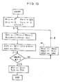
- Fig. 13 shows a flowchart for determining a solution of the key equation using Euclid's algorithm.
- the symbol [.] means a quotient of division.
- the error value e i at the error location i will be determined from the error locator polynomial ⁇ (z) obtained from Euclid's algorithm, the error evaluator polynomial ⁇ (z), and the error location i obtained from Chien's algorithm. From Eqs.
- the error locator polynimial ⁇ (z) and the error evaluator polynomial ⁇ (z)
- Fig. 14 shows, in block, a conventional decoder consisting of a multi-stage shift register 109 for delaying the received coded word, an adder 110, a syndrome computation circuit 111, an error locator polynomial deriving circuit 112, a Chien search circuit 113, a synchronizing circuit 114, a sequence control circuit 115, an input terminal 116 for receiving coded words, and an output terminal 117 for sending the corrected information.
- the synchronizing circuit detects the head of the received coded word. In response to the detected result, the sequence control circuit 115 starts operation.
- the received coded word is also put into the syndrome computation circuit 111 and the mult-stage shift register 109.
- the computed syndrome from the circuit 111 is fed to the error locator polynomial deriving circuit 112 to provide an error locator polynomial, which is then fed to the Chien search circuit 113 for performing Chien search.
- the output at the terminal 302 becomes zero.
- ⁇ i is a root of ⁇ (x).
- This process is called Chien search.
- the received coded word is output from the multi-stage shift register 203 in sequence from the head. This output is synchronized with the Chien search operation performed in the circuit 113.
- the output of the multi-stage shift register 203 is corrected in the correction circuit 206.
- Fig. 16 shows a conventional composite circuit having both syndrome and Chien search circuits.
- a syndrome is processed as follows.
- a succession of 8-bit words received at the input terminal 301 are fed through a switch Sx and the adders A0, A1, ... A15 in a Galois field GF(28) to an array of 8-bit registers L0, L1, ... L15, which have been cleared, for latching.
- the latched contents of the registers L1, L2, ..., L15 are multiplied by constants ⁇ , ⁇ 2, ..., ⁇ 15 in the Galois field GF(28) in the multipliers B1, B2, ... B15 and fed to the adders A1, A2 ...
- A15 for calculating the sums with the next input at the terminal 301 The sums are latched in the registers L1, L2, ... L15.
- the content in the register L1 is added to the next input without multiplication in the adder A0 and the sum is latched in the register L0.
- the switches S w0 , S w1 , ... S w15 are turned to the contacts U so that the calculated syndromes are shifted through the registers L0, L1, ... L15 in sequence and output at the terminal 303.
- the Chien search is performed as follows.
- the contents of the registers L0, L1, ... L8 are fed to a summing circuit 304 for providing the sum of the Chien algorithm at the output terminal 302.
- the above conventional decoder has the following shortcomings.
- the error locator polynomial deriving circuit becomes complicated for the long coded word, requiring a large number of stages of the multi-stage shift register.
- the degree of a polynomial is determined by a device consisting of arithmetic units, thus reducing the number of steps in the algorithm for determining the polynomial.
- the received word is stored in the memory, and the address of the memory is designated on the basis of the error location from the Chien search circuit to correct the received word at the address thereby eliminating the multi-stage shift register.
- the coefficient registers of a Chien search circuit and the adders for the elements of a Galois field are combined in such a manner that no computation is carried out for the element of the Galois field corresponding to the error location that does not exist.
- the decoder and encoder share some hardware so as to provide a compact system.
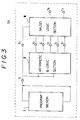
- Fig. 1 is a block diagram of a decoder system embodying the present invention.
- Fig. 2 is a block diagram of the syndrome Chien search computation circuit for the system of Fig. 1.
- Fig. 3 is a block diagram of the finite field logic circuit for the system of Fig. 1.
- Fig. 4 is a block diagram of the program section of the finite field logic circuit of Fig. 3.
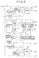
- Fig. 5 is a block diagram of the arithmetic and logic section of the system of Fig. .
- Fig. 6 is a block diagram of the Galois logic section of Fig. 3.
- Fig. 7 is a block diagram of the Galois logic unit for use in the Galois logic section of Fig. 6.
- Fig. 8 is a logic circuit diagram of the degree latch circuit for use in the arithmetic and logic section of Fig.5.
- Fig. 9 is an example of a logic circuit diagram of the square circuit of the Galois logic unit of Fig. 7 .
- Figs. 10(A) and (B) are charts showing the contents of RAM memories Ma and Mb and a register file to be updated according to the algorithm.
- Fig. 11 is a detailed block diagram of the Chien search circuit of Fig. 1 .
- Fig. 12 is a block diagram of a circuit used as both syndrome computation circuit and check symbol computation circuit for coding.
- Fig. 13 is a flowchart showing the algorithm for determining an error location in the Chien circuit.
- Fig. 14 is a block diagram of a conventional decoder.
- Fig. 15 is a block diagram of a conventional Chien circuit.
- Fig. 16 shows a circuit used as both conventional syndrome computation and Chien search circuits.
- a decoder system consists of a finite field logic circuit 123 for calculating a finite field such as deriving an error locator or evaluator polynomial, a delay memory 124 for storing a receiving code word, a syndrome/Chien search computation circuit 125 for carrying out syndrome computation or Chien search operation, and a control circuit 126 for monitoring the finite field logic circuit 123, the syndrome/Chien search computation circuit 125 and the delay memory 124 to control them and adjust the transfer of data between them upon coding or decoding and store an error location address output from the syndrome/Chien search computation circuit.
- a finite field logic circuit 123 for calculating a finite field such as deriving an error locator or evaluator polynomial
- a delay memory 124 for storing a receiving code word
- a syndrome/Chien search computation circuit 125 for carrying out syndrome computation or Chien search operation
- a control circuit 126 for monitoring the finite field logic circuit 123, the syndrome/Chi
- the syndrome/Chien search computation circuit 125 consists of a syndrome/Chien search logic section 118 having the same function as that of the conventional circuit and an address generation circuit 119 operable in synchronism with the Chien search logic circuit 118.
- This address generation circuit 119 is arranged in the form of a subtraction-type counter circuit.
- the syndrome/Chien search circuit 125 also has a clock input terminal 120, an output terminal 121 of the address generation circuit 119, and an output 122 which indicates that the output at the terminal 121 has detected the root of an error locator polynomial.
- the finite field logic circuit 123, the delay memory 124, and syndrome/Chien search logic circuit 125 are connected to data and control buses 127 and 128, respectively.
- a port of the memory 124 is connected to an external data bus 129 for input of a received coded word and output of the corrected word.
- a received coded word is fed to the delay memory 124 through the external data bus 129.
- the coded word is then fed to the syndrome/Chien search computation circuit 125 to provide a syndrome, from which the finite field logic circuit 123 derives error locator and evaluator polynomials.
- the error locator polynomial is fed to the syndrome/Chien search logic section 118 for performing Chien search to feed the finite field logic circuit 123 with an address corresponding to a root of the error locator polynomial.
- the address generation circuit 119 for outputting the address operates as a subtraction counter in synchronism with the syndrome/Chien search logic circuit 118.
- the finite field logic circuit 123 calculates an error value from the Chien search result and corrects the content at the error location address of the delay memory 124 which has been received from the syndrome/Chien search computation circuit 125.
- the data and control signals in the above operation are transferred through the data bus 127 and control bus 128. Then, the corrected content is output on the external bus 129 through the memory 124.
- the address generation circuit 119 operates in synchronism with the syndrome/Chien search circuit 118 to calculate an error location address in the memory 124, and the error correction code can be decoded throuth the finite field logic circuit 123 or delay memory 124 for storing the received coded word so that the multi-state shift register used in the conventional technology can be eliminated.
- the invention can be applied to the decoding of a binary coded word requiring no such computation.
- the content of the delay memory 124 may be inverted by using the address output from the syndrome/Chien search computation circuit 125.
- Fig. 3 there is shown a finite field logic circuit consisting of a program section I, an arithmetic and logic section II, and a Galois logic section III.
- a jump address setting circuit 1 is provided to set an address to which an operation jumps.
- a program counter 2 has addresses from 0 through 1023 and enables either conditional or unconditional jump depending on the flag status.
- a program ROM 3 contains an execution control program.
- a latch circuit 4 stores commands.
- Fig. 5 shows, in the arithmetic logic section II, counters 5 and 6 are adapted to count up to 81 or down to 0.
- Address data latch circuits 7 and 8 are used for addresses of the index system, for example.
- Address adders 9 and 10 are of the 6-bit configuration, for example.
- the above jump setting circuit includes the start, reset, and control circuits of the decoder and permits conditional jump depending on the external or internal flag status.
- FIG. 6 shows, in the Galois logic section III, flag registers F1 and F2 are used for generally input and output purposes, respectively.
- RAM A 11 and RAM B 12 are working random access memories.
- FIG. 5 there is shown an arithmetic and logic unit (ALU) 13.
- a register file 14 has a capacity of 5 bits x 4 words and four addresses AD1, AD2, AD3, and AD4, for example.
- a degree latch circuit 15 feeds the register file 14 with a write inhibit signal in response to a specified flag.
- a selector 16 is provided to select data lines (Ca, A, P, Cb).
- Registers 17 and 18 are provided to select and latch data lines (R, A, P) fed to the ALU 13.
- A stands for data for the ALU 13, P preset data, Ca a value of the counter 5, Cb a value of the counter 6, R a value of the register file 14.
- Flag registers F3 and F4 store the statuses of the counters, respectively.
- a Galois logic unit (GLU) 19 has a logic processor 20 for performing operations X + Z, X/Y, X.Y + Z, and X2 ⁇ Y + Z in the Galois field.
- F5 is a status flag output from the GLU 19
- F6 and F7 are status flags output from the ALU 13.
- An inverse element ROM 21 is a ROM for division in the Galois field and has a capacity of 256 bites in this embodiment.
- Registers 22, 23, and 24 are provided to select and latch data lines (P, A, B) to be fed to the GLU 19.
- P stands for preset data
- a and B are contacts for selecting data from RAM 11 and RAM 12, respectively.
- Selecters 25 and 26 have an input terminal I to which data is fed from the outside such as the syndrome or Chien search circuit and a terminal V to which the computation result of the GLU 19 is fed.
- a selector 27 is for data lines (V, A, B, R) output to the bus.
- St, Er, and Ew are flag registers for indicating whether or not the unit is under operation, there is a demad for reading from the bus, and there is a demand for outputting data to the bus, respectively.
- Fig. 7 there is shown the GLU 19 consisting of a square circuit 28, five selectors 29, 30, 31, 32, and 33, a multiplying circuit 34 in the Galois field, an adding circuit 35 in the Galois field, and a latch memory 36.
- Fig. 8 there is shown the degree latch circuit 15 consisting of a terminal M1 to which a degree latch command is fed, four terminals W1, W2, W3, and W4 to which respective write commands at addresses AD1, AD2, AD3, and AD4 are fed, a flag signal input terminal FL, four terminals EN1, EN2, EN3, and EN4 to which respective write enable signals at addresses AD1, AD2, AD3, and AD4 are fed, four flip-flops R1, R2, R3, and R4, five gate circuits G1, G2, G3, G4, and G5, a clock input terminal T, and a reset signal input terminal R.
- Fig. 9 there is shown the square circuit where an element X in the Galois field input at terminals A0, A1, ... A7 is squared and the value X2 is output at terminals Y0, Y1, ... Y7.
- the number adjacent to / means the number of leads. For example, /6 indicates six parallel leads.
- the index registers ADLA 7 and ADLB 8 are used so that M2(z), U1′(z), M1(z), and U2(z) may not overlap.
- the coefficients S15, S14, ..., S1, S0 latched in the register 24 are fed to the RAM A 11 as they are.
- the GLU 19 finds that the coefficient of S(z) is not '00', it feeds '1' to the flag register F5.
- the operation of the degree latch circuit a feature of the invention, will be described.
- An example of the degree latch circuit is shown in Fig. 8.
- the signal '1' at the terminals W1, W2, W3, or W4 means a write command at AD1, AD2, AD3, or AD4 of the register file 14, and the signal '0' at the output terminal EN1, EN2, EN3, or EN4 makes AD1, AD2, AD3, or AD4 write enable.
- the following procedure may be employed.
- a signal '1' is fed to the terminal MI before the coefficients of S(z) are fed to the register 24.
- the flag input terminal FL is connected to the flag register F5 at the terminal T5 and has an output '0'.
- a signal '1' is fed to the terminal W1 for writing at AD1.
- the input '1' to the terminal M1 is latched in the flip-flop R1 in timing with the clock T. If the output Q of the flip-flop R1 is '0' or its output QC is '1', the gate G1 outputs '1' unconditionaly so that the output terminal EN1 always outputs '0' when the input terminal W1 is '1', thus becoming write enable.
- the flip-flops R2 and R3 are kept under the reset condition.
- S(z) is fed to the GLU 19 and the flag register F5 becomes '1' when the first non-zero data is input.
- the flip-flop R2 latches '1' at the time of rise of a clock pulse T.
- the data of the counter 5 is latched at AD1 of the register file 14. The data then is the highest degree of S(z).
- the flip-flop R2 changes its Q from '0' to '1'. This signal change feeds '1' to the clock terminal of the flip-flop R3, which in turn changes its output QC to '0' and keeps it until a reset signal is fed to the flip-flop.
- This signal change to '0' at QC makes the gate G1 output '0'.
- This is a write inhibit command on the register file 14, thus turning the write enable terminals EN1, EN2, EN3, and EN4 to '1' regardless of the conditions of the write command input terminals W1, W2, W3, and W4. Consequently, no writing operation is carried out in the register file 14.
- This condition is matintained until the command on the degree latch circuit is released or the terminal M1 receives '0' to permit the flip-flop R1 to latch '0', so that the highest degree of S(z) is stored at AD1 of the register file 14.
- a configuration of the GLU 19 is shown in Fig. 7.
- a square circuit 28 in the Galois field is composed of a group of gates so as to output X2 when an element X in the Galois field is input.
- GF(28) for example, it is a logic circuit such as shown in Fig. 9.
- An inverse element ROM circuit 21 is designed to output Y ⁇ 1 when an element Y in the Galois field is input as an address.
- a multiplying circuit 34 in the Galois field is composed of a group of gates so as to output a product of the outputs from selectors 29 and 30.
- An addition circuit 35 in the Galois field is composed of a group of gates arranged in the form of an exclusive OR logic so as to output a sum of the outputs from the register 24 and the selecter 29.
- the registers X 22 and Y 23 are cleared.
- the coefficient of the highest degree of a polynomial M1(z) is fed to the register X 22 and the coefficients of a polynomial M2(z) is fed to the register Y 23 to perform a division X/Y.
- This output is the coefficient of the highest degree of a quotient polynomial Q(z).
- the highest degree of the quotient polynomial Q(z) can be obtained by feeding the register T 18 with the highest degree of M1(z) stored at AD2 of the register file 14 and the register U 17 with the highest degree of M2(z) stored at AD1 of the rester file to perform a subtraction T - U in the ALU 13. This result is stored at AD4 of the register file 14.
- the coefficients of the above quotient polynomial Q(z) are latched in the register Y 23, and the coefficients of degrees lower than the highest degree of M2(z) are fed to the register X 22 in the order of degree and the coefficients of degrees lower than the highest degree of M1(z) are fed to the register Z 24 in the order of degree for performing a product and addition operation X′Y + Z to find a remainder polynomial for the coefficients of Q(z).
- the degree latch circuit is operated to store the highest degree of the remainder polynomial at AD2 of the register file 14.
- the obtained polynomial is also overwritten on the RAM B 12 which stores M1(z).
- '00' is written at the address where the coefficient of the highest degree of M1(z) is stored.
- the coefficient data of Q(z) latched in the register Y 23 are latched as they are, the coefficients of U1′(z) is fed to the register X 22 in sequence from the highest degree, and the coefficients of U2(z) are fed to the register Z 24 in sequence from the higherst degree of the output polynomial to perform an operation X ⁇ Y + Z in the GLU 19 and overwrite the output on the RAM B 12 where U2(z) has been stored.
- the degree data of R(z) or data at AD2 of the register file 14 is fed to the register U 17 and the constant t-1 is fed to the register T 18 to perform an operation T - U in the ALU 13.
- the flag register F7 makes a true or false decision under any of conditions T ⁇ U, T > U, T ⁇ U, or T ⁇ U. In a case of true, it outputs '1'.
- T ⁇ U is selected. Let us examine the flag register F7 with respect to the T - U computation results.
- the flag register F7 is connected to the input of the jump address setting circuit 1 so that when the flag F7 is '1' in response to a conditional jump command, it jumps and leaves the repeatitive loop. If the flag F7 is '0' or R(z) > t - 1, the afore-mentioned operation will be repeated after the operation W of Fig. 13. However, this requires only apparent change of the data assignments in the RAMs 11 and 12 and the register file 14. That is, in the second cycle of operation, the data output from the RAM A 11 in the first cycle of operation is output from the RAM B 12 and the data from the RAM B 12 is output from the RAM A 11.
- the data to the RAM A 11 is fed to the RAM B 12 and the data to the RAM B 12 is fed to the RAM A 11 to exchange the data assignments at AD1 and AD2 of the register file 14 without changing the operation.
- the operation speed is increased by providing two RAMs to eliminate the data transfer.
- the operation requiring at least three steps with the aid of a single RAM can be made in two steps by reading the input data from the first RAM and feeding the operational result to the second RAM to increase the operational speed.
- the respective data assignments in the RAMs A 11 and B 12 and the register file 14 in the second cycle at the points of j and l are shown in the columns d and e of Fig. 10, respectively.
- the data assignments at the points j and l in the even or odd numbers of cycles are shown in the columns f and g or h and i of Fig. 10, respectively.
- the data assignments when the highest degree of R(z) is below t - 1 and the operation leaves the loop is shown in the column j of Fig.10.
- ⁇ (z) and ⁇ (z) are always stored in the RAM A 11.
- the error location i and the element ⁇ i indicating the location i in the Galois field are determined by performing a Chien search based on the obtained error locator polynomial ⁇ (z).
- the error value is determined from the obtained error locator polynomial ⁇ (z), error evaluator polynomial ⁇ (z), and the Galois element ⁇ i . As shown in Eqs.
- E be a set of error locations, then Hence, the Chien search has no influence on K.
- the determination of the degree of a polynomial is speeded up by using the common arithmetic units, and the process is accelerated by means of a latch circuit for latching the degree data which are required for the execution of polynomial computation.
- the conventional GLU can perform only a product X ⁇ Y, addition X + Y, or division X/Y at a step of operation, but, according to the invention, the operation X ⁇ Y + Z or X2 ⁇ Y + Z in the Galois field can be carried out quickly in a single step by using a multiplying or squaring circuit which is able to execute in a single step. Since a pair of RAMs are provided in the GLU to increase the process speed, a decoder with a large minimum distance ( d ⁇ 10 - 30) is possible.
- the syndrome computation and Chien search operation in the syndrome/Chien search logic section 118 will be described with reference to Fig. 16.
- the registers L0 through L15 are cleared.
- the switch Sx is then turned on and the switches SW0 through SW15 are turned to the W side.
- the received data are successively fed to the input terminal 301.
- the output syndromes are put into the finite field logic circuit 123 via the data bus 127 in Fig. 1, where an error locator polynomial ⁇ (z) and an error evaluator polynomial ⁇ (z) are determined.
- this may be obtained by combining the coefficients of the error locator polynomial and the elements of the Galois field in such a manner that coefficients ⁇ t , ⁇ t-1 , ..., ⁇ 0 may correspond to the ⁇ 0 multiplier, ⁇ 1 multiplier, ... , ⁇ t multiplier.
- Eq. 54 is recurrently calculated to output an error location corresponding ⁇ -i at which the sum is zero.
- Eq. 53 shows, computation is performed in the order from the location 255 to the location 0.
- the registers L0 to L15 are cleared in advance. Also, the switch Sx is turned off and the switches SW0 to SW15 are turned to the U side. Then, the coefficients of ⁇ (z) are fed to the input terminal 301 in succession from the top degree and the registers L0 to L15 are right shifted until ⁇ t is put into the register L0. At this point, the switches SW0 to SW15 are turned to the W side.
- the registers L0, L1, .... L t latch ⁇ t , ⁇ t-1 , ... , ⁇ 0, respectively.
- the registers L0 to L t in Fig. 16 correspond to K0 to K t , respectively, in Fig. 11 and similarly, the finite field frequency multiplier Bi to B t correspond to M1 to M t , respectively.
- the ⁇ 0 multiplier may be merely a line.
- the sum circuit 304 is equivalent to the adder. In this case, adder is in the Galois field
- the registers L t+1 to L8 are connected to the input of the sum circuit 304 but they latch zero and have no influence on the Chien search.
- the outputs of the sum circuit 304 are put into the zero decision circuit 4A. In the case of all zeros, a flag is generated at the output terminal 122.
- the address generator circuit 119 calculates the location address in the delay memory in synchronism with the Chien search.
- the flag signal and the location address are put into the control circuit 126 via the control data bus 128 in Fig. 1.
- the control circuit 126 stores the location address and, when the Chien search is completed, puts the element of a finite field corresponding to the error location into the finite field logic circuit 123 via the data bus 127.
- the finite field logic circuit 123 determines the error value from the error locator polynomial ⁇ (z) and the error evaluator polynomial ⁇ (z) for making correction.
- the decoder system of Fig. 1 completes decoding.
- encoding is carried out in the syndrome/Chien search computation circuit of Fig. 1; the syndrome/Chien search logic operation is carried out by the syndrome/Chien search computation circuit 125 of Fig. 1.
- the rest of the logic operation is performed by the finite field logic circuit 123. More specifically, the syndromes output from the syndrome/Chien search computation circuit 125 are put into the finite field logic circuit 123.
- the input syndromes are stored in the RAM A 11 of Fig. 6. This is comparable to the fact that the syndromes are stored in the syndrome computation section 316 of Fig. 12.
- the data which have been stored in the first memory of Fig. 12, are put into the register Y 23 in succession.
- the syndrome data in the RAM A 11 are put into the register X 22, and the RAM B 12 is assigned in place of the second memory 314 of Fig. 12. These data are put into the register Z 24 to perform a finite field logic X Y + Z in the GLU 20. The results are fed back to the RAM B 12 to determine the check symbol data in the same manner as in the circuit of Fig. 12.
- the received word vector r is given by where r i is the information symbol section, r c is the check symbol section, and 0 c and 0 i are zero symbols.
- the second memory 314 which has been cleared in the initial condition, cooperates with the adder 313 to calculate respective terms of A ⁇ 1 and S i to give an accumlative sum for each term.
- the register 315 latches a check symbol r c , which is then output at the terminal 310.
Landscapes
- Physics & Mathematics (AREA)
- Mathematical Physics (AREA)
- Probability & Statistics with Applications (AREA)
- Engineering & Computer Science (AREA)
- Theoretical Computer Science (AREA)
- Algebra (AREA)
- General Physics & Mathematics (AREA)
- Pure & Applied Mathematics (AREA)
- Error Detection And Correction (AREA)
Claims (8)
- Ein Fehlerkorrekturkodier/Dekodiersystem mit einem Speicher zum Speichern eines aufgenommenen kodierten Wortes,
einem Finiten-Feld-Logik-Schaltkreis zum Ableiten eines Fehlerstellenpolynoms und einem Fehlerauswertepolynom aus dem aufgenommenen Wort, wobei der Finite-Feld-Logik-Schaltkreis umfaßt:- arithmetische und logische Mittel zum Bestimmen der Grade der beiden Polynome, wobei die arithmetischen und logischen Mittel einen Speicher zum Speichern von Zwischendaten in der Berechnung beider Polynome besitzen,- Galois-logischen Mittel, die empfänglich sind für diese Grade, um die beiden Polynome zur Korrektur eines Fehlers zu lösen, und- Program-Mitteln zum Steuern der Galois-logischen Mittel und der arithmetischen und logischen Mittel,einem Syndrom/Chiensuch-Berechnungsschaltkreis zum Bestimmen eines Syndroms und einer Fehlerstelle aus den Ergebnissen, die von dem Finiten-Feld-Logik-Schaltkreis ausgegeben sind, und
einem Adresserzeugungs-Schaltkreis, der in Form eines Zählschaltkreises des Subtraktionstyps angeordnet ist, der auf eine Fehlerstelle empfänglich ist, um eine Adresse in dem Speicher zu erzeugen, so daß das aufgenommene Wort an der Adresse geholt und korrigiert werden kann und der synchron mit dem Syndrom/Chiensuch-Berechnungsschaltkreis arbeitet. - Ein Fehlerkorrektur/Kodier/Dekodiersystem nach Anspruch 1, dadurch gekennzeichnet, daß die Galois-logischen Mittel drei logische Register und zwei Mehrzweckspeicher besitzen.
- Ein Fehlerkorrekturkodier/Dekodiersystem nach Anspruch 1, dadurch gekennzeichnet, daß die Galois-logischen Mittel eine Fehlerstelle αi bestimmen und ein Fehlermuster ei ohne Normalisierung des Auswertungspolynoms

- Ein Fehlerkorrekturkodier/Dekodiersystem nach Anspruch 1, dadurch gekennzeichnet, daß die Galois-logischen Mittel einen Quadrierschaltkreis in einem Galoisfeld haben.
- Ein Fehlerkorrekturkodier/Dekodiersystem nach Anspruch 1, dadurch gekennzeichnet, daß der Speicher der Arithmetik- und Logikmittel ein Grad-Zwischenspeicher-Schaltkreis zum Verhindern jeglichen Schreibens auf den Speicher besitzt, wenn ein vorbestimmter Zustandsmerker in einem vorbestimmten Intervall gesetzt ist.
- Ein Fehlerkorrekturkodier/Dekodiersystem nach Anspruch 1, dadurch gekennzeichnet, daß- die Galois-logischen Mittel einen ersten Mehrzweckspeicher und- einen zweiten Mehrzweckspeicher haben,wobei die arithmetischen und logischen Mittel einen Speicher zum Zwischenspeichern eines Grades eines Polynoms besitzen,
wobei die ersten und zweiten Mehrzweckspeicher so angeordnet sind, daß eine Dateneingabe von dem ersten Mehrzweckspeicher in den zweiten Mehrzweckspeicher im nächsten Arbeitsschritt eingegeben werden kann,
die Dateneingabe aus dem zweiten Mehrzweckspeicher in den ersten Mehrzweckspeicher im nächsten Arbeitsschritt eingegeben werden kann, und
daß der Speicher der arithmetischen und logischen Mittel Datenzuordnungen zu einer ersten Adresse und einer zweiten Adresse für ein Vorgehen ohne jeglichen Datentransfer austauschen kann. - Ein Fehlerkorrekturkodier/Dekodiersystem nach Anspruch 1, dadurch gekennzeichnet, daß der Syndrom/Chiensuch-Berechnungsschaltkreis zur Bestimmung einer Fehlerstelle von beiden Polynomen enthält:
einen Addierer zum Berechnen von

einen Entscheidungsschaltkreis zum Entscheiden, ob die Gleichung
- Ein Fehlerkorrekturkodier/Dekodiersystem nach Anspruch 1, dadurch gekennzeichnet, daß der Syndrom/Chiensuch-Berechnungsschaltkreis enthält:- einen ersten Speicher zum Speichern vorbestimmter Konstanten,- einen Multiplizierschaltkreis zum Multiplizieren einer Syndromausgabe aus den Syndromberechnungsmitteln mit Konstanten, die aufeinanderfolgend aus dem ersten Speicher eingelesen sind, und- einen Summierschaltkreis zum Aufsummieren der Multiplikationsergebnisse in Reihenfolge aus den Multiplikationsschaltkreisen, um hiervon die Summe zu erhalten, um so ein Prüfsymbol zur Informationseingabe an die Syndromberechnungsmittel zu geben.
Applications Claiming Priority (6)
| Application Number | Priority Date | Filing Date | Title |
|---|---|---|---|
| JP61141679A JPS6379423A (ja) | 1986-06-18 | 1986-06-18 | チエンサ−チ回路 |
| JP141679/86 | 1986-06-18 | ||
| JP168402/86 | 1986-07-17 | ||
| JP16840286A JPH0744467B2 (ja) | 1986-07-17 | 1986-07-17 | 符号化回路 |
| JP240685/86 | 1986-10-08 | ||
| JP61240685A JPS6394720A (ja) | 1986-10-08 | 1986-10-08 | 誤り訂正符号の復号化回路 |
Publications (3)
| Publication Number | Publication Date |
|---|---|
| EP0249982A2 EP0249982A2 (de) | 1987-12-23 |
| EP0249982A3 EP0249982A3 (en) | 1990-12-27 |
| EP0249982B1 true EP0249982B1 (de) | 1994-09-14 |
Family
ID=27318297
Family Applications (1)
| Application Number | Title | Priority Date | Filing Date |
|---|---|---|---|
| EP87108796A Expired - Lifetime EP0249982B1 (de) | 1986-06-18 | 1987-06-19 | Dekodierer |
Country Status (4)
| Country | Link |
|---|---|
| US (1) | US4841300A (de) |
| EP (1) | EP0249982B1 (de) |
| CA (1) | CA1291819C (de) |
| DE (1) | DE3750526T2 (de) |
Families Citing this family (19)
| Publication number | Priority date | Publication date | Assignee | Title |
|---|---|---|---|---|
| FR2625055B1 (fr) * | 1987-12-17 | 1993-09-24 | Alcatel Thomson Faisceaux | Procede de detection d'effacements affectant une liaison hertzienne numerique et chaine de reception mettant en oeuvre un tel procede |
| DE68920142T2 (de) * | 1989-08-24 | 1995-07-13 | Philips Electronics Nv | Verfahren und Einrichtung zur Decodierung von wortgeschützten Codewörtern durch einen nichtbinären BCH-Code gegen mindestens einen Symbolfehler. |
| US5099482A (en) * | 1989-08-30 | 1992-03-24 | Idaho Research Foundation, Inc. | Apparatus for detecting uncorrectable error patterns when using Euclid's algorithm to decode Reed-Solomon (BCH) codes |
| JP2504312B2 (ja) * | 1990-08-29 | 1996-06-05 | 三菱電機株式会社 | プライオリティエンコ―ダ及びそれを備えたデ―タ処理装置 |
| US5343481A (en) * | 1991-01-07 | 1994-08-30 | Kraft Clifford H | BCH error-location polynomial decoder |
| EP0611054B1 (de) * | 1993-01-22 | 1998-04-08 | Canon Kabushiki Kaisha | Vorrichtung und Verfahren zur Ableitung von Polynomialmengen |
| DE69414631T2 (de) * | 1993-03-31 | 1999-04-08 | Kabushiki Kaisha Toshiba, Kawasaki, Kanagawa | Schaltung zur Durchführung des Euclidschen Algorithmus bei der Dekodierung Arithmetischer Kodes |
| US5463642A (en) * | 1993-06-29 | 1995-10-31 | Mitsubishi Semiconductor America, Inc. | Method and apparatus for determining error location |
| JP3160448B2 (ja) * | 1993-11-30 | 2001-04-25 | 富士通株式会社 | データ訂正装置 |
| US5642367A (en) * | 1994-02-07 | 1997-06-24 | Mitsubishi Semiconductor America, Inc. | Finite field polynomial processing module for error control coding |
| JPH10112659A (ja) * | 1996-10-08 | 1998-04-28 | Canon Inc | 誤り訂正復号装置 |
| JP3850511B2 (ja) * | 1997-05-07 | 2006-11-29 | 日本テキサス・インスツルメンツ株式会社 | リードソロモン復号装置 |
| US6154868A (en) * | 1997-07-18 | 2000-11-28 | International Business Machines Corporation | Method and means for computationally efficient on-the-fly error correction in linear cyclic codes using ultra-fast error location |
| US6154869A (en) * | 1998-02-03 | 2000-11-28 | Texas Instruments Incorporated | Combined error position circuit and chien search circuit for reed-solomon decoding |
| US6374383B1 (en) * | 1999-06-07 | 2002-04-16 | Maxtor Corporation | Determining error locations using error correction codes |
| EP1460765A1 (de) * | 2003-03-19 | 2004-09-22 | STMicroelectronics S.r.l. | Fehlerkorrekturmethode für als Symbolsequenz codierte digitale Daten |
| JP4891704B2 (ja) * | 2006-08-28 | 2012-03-07 | 株式会社東芝 | 半導体記憶装置 |
| JP5259343B2 (ja) * | 2008-10-31 | 2013-08-07 | 株式会社東芝 | メモリ装置 |
| US9954553B1 (en) * | 2015-06-05 | 2018-04-24 | Altera Corporation | Circuitry and methods for continuous parallel decoder operation |
Family Cites Families (9)
| Publication number | Priority date | Publication date | Assignee | Title |
|---|---|---|---|---|
| US4099160A (en) * | 1976-07-15 | 1978-07-04 | International Business Machines Corporation | Error location apparatus and methods |
| US4162480A (en) * | 1977-01-28 | 1979-07-24 | Cyclotomics, Inc. | Galois field computer |
| US4142174A (en) * | 1977-08-15 | 1979-02-27 | International Business Machines Corporation | High speed decoding of Reed-Solomon codes |
| US4389636A (en) * | 1980-11-03 | 1983-06-21 | Riddle H S Jun | Encoding/decoding syncronization technique |
| JPS5992688A (ja) * | 1982-11-19 | 1984-05-28 | Fuji Photo Film Co Ltd | 適応形画像圧縮方式 |
| US4567594A (en) * | 1983-06-07 | 1986-01-28 | Burroughs Corporation | Reed-Solomon error detecting and correcting system employing pipelined processors |
| US4605921A (en) * | 1983-06-20 | 1986-08-12 | Riddle Herbert S | Digital word-framing technique and system |
| US4584686A (en) * | 1983-12-22 | 1986-04-22 | Optical Storage International | Reed-Solomon error correction apparatus |
| US4649541A (en) * | 1984-11-21 | 1987-03-10 | The United States Of America As Represented By The Administrator Of The National Aeronautics And Space Administration | Reed-Solomon decoder |
-
1987
- 1987-06-17 US US07/063,178 patent/US4841300A/en not_active Expired - Lifetime
- 1987-06-18 CA CA000540041A patent/CA1291819C/en not_active Expired - Lifetime
- 1987-06-19 EP EP87108796A patent/EP0249982B1/de not_active Expired - Lifetime
- 1987-06-19 DE DE3750526T patent/DE3750526T2/de not_active Expired - Fee Related
Also Published As
| Publication number | Publication date |
|---|---|
| US4841300A (en) | 1989-06-20 |
| DE3750526T2 (de) | 1995-01-12 |
| EP0249982A2 (de) | 1987-12-23 |
| EP0249982A3 (en) | 1990-12-27 |
| CA1291819C (en) | 1991-11-05 |
| DE3750526D1 (de) | 1994-10-20 |
Similar Documents
| Publication | Publication Date | Title |
|---|---|---|
| EP0249982B1 (de) | Dekodierer | |
| US4099160A (en) | Error location apparatus and methods | |
| EP0167627B1 (de) | Verfahren und vorrichtung zur dekodierung eines fehlerverbesserungskodes | |
| US5517509A (en) | Decoder for decoding ECC using Euclid's algorithm | |
| US5715262A (en) | Errors and erasures correcting reed-solomon decoder | |
| US5170399A (en) | Reed-Solomon Euclid algorithm decoder having a process configurable Euclid stack | |
| US6374383B1 (en) | Determining error locations using error correction codes | |
| US4958349A (en) | High data rate BCH decoder | |
| US6347389B1 (en) | Pipelined high speed reed-solomon error/erasure decoder | |
| US5440570A (en) | Real-time binary BCH decoder | |
| US20030192007A1 (en) | Code-programmable field-programmable architecturally-systolic Reed-Solomon BCH error correction decoder integrated circuit and error correction decoding method | |
| US5805617A (en) | Apparatus for computing error correction syndromes | |
| JP3176171B2 (ja) | 誤り訂正方法及びその装置 | |
| JPH0452556B2 (de) | ||
| US7089276B2 (en) | Modular Galois-field subfield-power integrated inverter-multiplier circuit for Galois-field division over GF(256) | |
| US5365529A (en) | Circuitry for detecting and correcting errors in data words occurring in Reed-Solomon coded blocks and determining when errors are uncorrectable by syndrome analysis, Euclid's algorithm and a Chien search | |
| EP0836285B1 (de) | Reed-Solomon Dekodierer mit universeller Prozessoreinheit und speziellen Schaltungen | |
| EP0393080B1 (de) | Hypersystolischer reed-solomon-encoder | |
| US5541937A (en) | Apparatus for uniformly correcting erasure and error of received word by using a common polynomial | |
| KR100258951B1 (ko) | 리드-솔로몬(rs) 복호기와 그 복호방법 | |
| EP0661841B1 (de) | Paritäts- und Syndromgenerator zur Fehler-Erkennung und -Korrektur in digitalen Übertragungssystemen | |
| EP0595326B1 (de) | Reed-Solomon Fehlerkorrektur mit Euclidschem Algorithmus | |
| EP1175015B1 (de) | Dekodierungsschaltkreis und zugehöriges Dekodierungsverfahren | |
| US6145112A (en) | Error correcting method and apparatus | |
| JP2575506B2 (ja) | チエンサーチ回路 |
Legal Events
| Date | Code | Title | Description |
|---|---|---|---|
| PUAI | Public reference made under article 153(3) epc to a published international application that has entered the european phase |
Free format text: ORIGINAL CODE: 0009012 |
|
| AK | Designated contracting states |
Kind code of ref document: A2 Designated state(s): DE FR GB NL |
|
| PUAL | Search report despatched |
Free format text: ORIGINAL CODE: 0009013 |
|
| AK | Designated contracting states |
Kind code of ref document: A3 Designated state(s): DE FR GB NL |
|
| 17P | Request for examination filed |
Effective date: 19901228 |
|
| 17Q | First examination report despatched |
Effective date: 19930430 |
|
| GRAA | (expected) grant |
Free format text: ORIGINAL CODE: 0009210 |
|
| AK | Designated contracting states |
Kind code of ref document: B1 Designated state(s): DE FR GB NL |
|
| REF | Corresponds to: |
Ref document number: 3750526 Country of ref document: DE Date of ref document: 19941020 |
|
| ET | Fr: translation filed | ||
| PLBE | No opposition filed within time limit |
Free format text: ORIGINAL CODE: 0009261 |
|
| STAA | Information on the status of an ep patent application or granted ep patent |
Free format text: STATUS: NO OPPOSITION FILED WITHIN TIME LIMIT |
|
| 26N | No opposition filed | ||
| PGFP | Annual fee paid to national office [announced via postgrant information from national office to epo] |
Ref country code: GB Payment date: 19960610 Year of fee payment: 10 |
|
| PGFP | Annual fee paid to national office [announced via postgrant information from national office to epo] |
Ref country code: FR Payment date: 19960611 Year of fee payment: 10 |
|
| REG | Reference to a national code |
Ref country code: GB Ref legal event code: 746 Effective date: 19960611 |
|
| REG | Reference to a national code |
Ref country code: FR Ref legal event code: D6 |
|
| PG25 | Lapsed in a contracting state [announced via postgrant information from national office to epo] |
Ref country code: GB Free format text: LAPSE BECAUSE OF NON-PAYMENT OF DUE FEES Effective date: 19970619 |
|
| GBPC | Gb: european patent ceased through non-payment of renewal fee |
Effective date: 19970619 |
|
| PG25 | Lapsed in a contracting state [announced via postgrant information from national office to epo] |
Ref country code: FR Free format text: LAPSE BECAUSE OF NON-PAYMENT OF DUE FEES Effective date: 19980227 |
|
| REG | Reference to a national code |
Ref country code: FR Ref legal event code: ST |
|
| REG | Reference to a national code |
Ref country code: FR Ref legal event code: ST |
|
| PGFP | Annual fee paid to national office [announced via postgrant information from national office to epo] |
Ref country code: DE Payment date: 20000619 Year of fee payment: 14 |
|
| PG25 | Lapsed in a contracting state [announced via postgrant information from national office to epo] |
Ref country code: DE Free format text: LAPSE BECAUSE OF NON-PAYMENT OF DUE FEES Effective date: 20020403 |
|
| PGFP | Annual fee paid to national office [announced via postgrant information from national office to epo] |
Ref country code: NL Payment date: 20030630 Year of fee payment: 17 |
|
| PG25 | Lapsed in a contracting state [announced via postgrant information from national office to epo] |
Ref country code: NL Free format text: LAPSE BECAUSE OF NON-PAYMENT OF DUE FEES Effective date: 20050101 |
|
| NLV4 | Nl: lapsed or anulled due to non-payment of the annual fee |
Effective date: 20050101 |