US4873688A - High-speed real-time Reed-Solomon decoder - Google Patents
High-speed real-time Reed-Solomon decoder Download PDFInfo
- Publication number
- US4873688A US4873688A US07/105,401 US10540187A US4873688A US 4873688 A US4873688 A US 4873688A US 10540187 A US10540187 A US 10540187A US 4873688 A US4873688 A US 4873688A
- Authority
- US
- United States
- Prior art keywords
- input
- polynomial
- output
- coupled
- multiplier
- Prior art date
- Legal status (The legal status is an assumption and is not a legal conclusion. Google has not performed a legal analysis and makes no representation as to the accuracy of the status listed.)
- Expired - Lifetime
Links
Images
Classifications
-
- H—ELECTRICITY
- H03—ELECTRONIC CIRCUITRY
- H03M—CODING; DECODING; CODE CONVERSION IN GENERAL
- H03M13/00—Coding, decoding or code conversion, for error detection or error correction; Coding theory basic assumptions; Coding bounds; Error probability evaluation methods; Channel models; Simulation or testing of codes
- H03M13/03—Error detection or forward error correction by redundancy in data representation, i.e. code words containing more digits than the source words
- H03M13/05—Error detection or forward error correction by redundancy in data representation, i.e. code words containing more digits than the source words using block codes, i.e. a predetermined number of check bits joined to a predetermined number of information bits
- H03M13/13—Linear codes
- H03M13/15—Cyclic codes, i.e. cyclic shifts of codewords produce other codewords, e.g. codes defined by a generator polynomial, Bose-Chaudhuri-Hocquenghem [BCH] codes
- H03M13/151—Cyclic codes, i.e. cyclic shifts of codewords produce other codewords, e.g. codes defined by a generator polynomial, Bose-Chaudhuri-Hocquenghem [BCH] codes using error location or error correction polynomials
- H03M13/1525—Determination and particular use of error location polynomials
- H03M13/1535—Determination and particular use of error location polynomials using the Euclid algorithm
Definitions
- This invention relates to the field of error correction in data. More particularly, this invention relates to system architecture for a high-speed real-time Reed-Solomon decoder used to correct errors in stored or transmitted data.
- Computers and other electronic equipment are useful for communicating, transmitting and storing information for retrieval at another location or later time.
- extrinsic noise introduced by the electronic system or external system can cause error to occur in the transmitted or stored information.
- Reed-Solomon (RS) codes are known and used for encoding and decoding information in such a way that induced errors are correctable. Such coding schemes are discussed in Error-Correction Coding for Digital Communications by George C. Clark, Jr. and J. Bibb Cain, published by the Plenum Press the contents of which are hereby incorporated by reference. The reader is directed to this book for additional information.
- a Galois Field error correction decoder which can correct an error in a received polynomial.
- the apparatus includes means for generating a plurality of syndrome polynomials.
- a magnitude polynomial, ⁇ (x), and a location polynomial, ⁇ (x), having a first derivative, ⁇ '(x), are calculated from the syndrome polynomials utilizing Euclid's Algorithm.
- the module utilizing Euclid's Algorithm includes a general Galois Field multiplier.
- the values of the magnitude polynomial ⁇ (x) is multiplied by a power of x and is divided by the first derivative of the location polynomial evaluated at various rulers of x to form a quotient.
- the division includes finding the inverse of the first derivative and multiplying the inverse by the value of the magnitude polynomial multiplied by a power of x.
- the error is corrected by Exclusive ORing the quotient with the received polynomial.
- FIG. 1 is a block diagram of a circuit which forms the dual basis of a Galois Field polynomial.
- FIG. 2 is a block diagram of a prior art syndrome generator.
- FIG. 3 is a block diagram of the general architecture of the error correction decoder of the preferred embodiment.
- FIG. 4 is a block diagram of a general Galois Field multiplier for 4 bit multiplicands.
- FIG. 6 is a more detailed block diagram of the circuit of FIG. 5.
- FIGS. 6a, 6b, and 6c which show alternate representations of the block diagrams of FIGS. 4, 5 and 6, respectively.
- FIG. 7 is a block diagram of the constant multiplier utilized in the syndrome generator of the preferred embodiment.
- FIG. 8 is a block diagram of the Euclid Divide module.
- FIG. 9 is a block diagram of Euclid Multiple module.
- FIG. 10 is a block diagram of the polynomial solver.
- the RS code used can be described with the following parameters and notation:
- Each RS code is an (n,k) code where k ⁇ n. This means that each code contains n total symbols but only k symbols of information. The remaining n-k symbols contain the coded information necessary to correct errors and are sometimes called parity symbols.
- the RS code block is defined to be
- G(x) Galois Field generator polynomial
- G(x) has zero roots at ⁇ 0 , ⁇ 1 , ⁇ 2 , . . . , ⁇ 2t-i .
- a more general form of the generator polynomial is described as ##EQU2## where s is an offset and ⁇ is another primitive element of the field equal to ⁇ i . Use of the offset s allows for the development of a more general purpose RS decoder.
- Each of the symbols of the RS code polynomial are members of the finite Galois Field.
- a Galois Field can be defined by an irreducible polynomial p(x). This polynomial has coefficients from the field GF(p) and is irreducible. The infinite set of all polynomials can be mapped into the finite field by the congruency
- the remainder of the division b(x)/p(x) is the field element a(x).
- the field element can be represented by the coefficients of a(x). If p is 2, then these coefficients are bits and the field elements in GF(2 q ) are q-bit binary words.
- Each Galois Field resulting from a different polynomial and/or a different primitive element has a different element sequence and may have a different number of elements.
- FIG. 1 A block diagram of a circuit for forming a dual polynomial is shown in FIG. 1.
- An input polynomial 20 is coupled to a constant multiplier 22 and to a multiplexer 24.
- the constant multiplier multiplies the input polynomial 20 by the linear operator T -1 .
- the output of the constant multiplier is also coupled to a separate input of the multiplexer 24.
- the dual basis control signal 26 determines whether the output polynomial 28 is the input polynomial 20 or the dual polynomial that is formed by the constant multiplier 22.
- E(x) is the error polynomial and each r i is a field element.
- the first step in the decoding algorithm is to calculate the syndromes.
- the 2t syndromes are ##EQU3## where 0 ⁇ k ⁇ 2t-1.
- the value of the syndrome polynomial can be defined as ##EQU4## Another equivalent definition of the syndrome polynomial is as follows.
- the syndrome polynomial is defined as
- the next step is to obtain the error location polynomial, ⁇ (x) and the error magnitude polynomial ⁇ (x). These polynomials have the following relationship with the syndrome polynomial
- the error location and error magnitude polynomials can be obtained by using Euclid's greatest common divisor algorithm, which is a recursive operation. The algorithm is described later.
- the location of the error is in symbol n-i of the received polynomial R(x).
- the magnitude of the error is
- ⁇ '(x) is the first derivative of ⁇ (x) with respect to x.
- the reader is referred to Clark and Cain.
- Cell interconnect is an important issue in efficient chip design. Interconnect can consume major portions of a chip layout and greatly limit the amount of circuitry that can be placed on a chip. An objective in the design here was to minimize the amount of cell interconnect.
- the VLSI cells used throughout the decoder include the following Galois Field processing elements: adder, constant multiplier, general multiplier, and field inverse.
- the constant multiplier performs the operation c ⁇ x, where c is a constant and x is a variable; the general multiplier performs the operation x1 ⁇ x2 on the Galois Field element variables x1 and x2.
- Addition in the Galois Field is the bitwise Exclusive OR of the field elements.
- ⁇ 6 is the Galois Field element representing the polynomial ⁇ 3 + ⁇ 2
- ⁇ 7 is ⁇ 3 + ⁇ +1
- ⁇ 13 is ⁇ 3 + ⁇ 2 +1 in the field defined in Table 1.
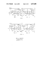
- FIG. 2 depicts the general structure used here to implement a constant multiplier.
- An input message symbol 42 is coupled into a Galois Field adder 43.
- the adder 43 is coupled to supply information to register 44.
- Register 44 is coupled to supply information to multiplier 45.
- the multiplier 45 is coupled to add information back into the adder 43.
- information stored in the register 44 is supplied to the output terminal 46.
- the general multiplier is a more complex module and was implemented with a pass transistor logic circuit that performs multiplication of two Galois Field polynomials.
- the method used to perform the inverse operation is to program a ROM with the necessary values to look up the reciprocal of a given field element. Division is performed by looking up the inverse and multiplying by the inverse.
- FIG. 4 shows a general Galois Field multiplier in GF(2 4 ).
- the individual multiply cells are formed into an array of 4 ⁇ 4 multiply cells.
- the cells are shown to be numbered M(x,y) where x represents the column and y represents the row.
- the feedback cells are included into the array of multiply cells as shown in FIG. 5.
- the feedback cells are labeled F.
- the ⁇ 3 column feeds into the ⁇ 0 column.
- the feedback cell feeds back into the ⁇ 1 column.
- FIG. 6 shows a more detailed block diagram of the circuit of FIG. 5.
- the multiplication is performed as follows.
- the 4 ⁇ 4 array of multiplier cells are numbered M(x,y) where x indicates column and y indicates row similar to FIGS. 4 and 5.
- the binary inputs for ⁇ and ⁇ are applied to the indicated inputs on the circuit schematic as FIG. 6.
- the inputs for ⁇ 0 through ⁇ 3 would allow the Galois Field addition of a third element to the product of ⁇ times ⁇ , i.e., ⁇ + ⁇ .
- the input ⁇ is a carry in which would allow two or more similar blocks of GS(2 4 ) general multipliers to be ganged together.
- the ⁇ s and ⁇ s are set to binary 0 input.
- the ⁇ input can be deleted rather than setting the input to 0 to achieve the same result.
- the multiplier of FIG. 6 can be generalized as shown in FIG. 6a and described as an efficient combinational circuit that can be described algorithmically.
- the multiplier performs the function
- ⁇ (x) and ⁇ (x) are the q bit multiplicands
- ⁇ (x) is the q bit addend
- w(x) is the q bit result
- q is the number of bits in the field.
- the general multiplier consists of q rows, with all of the rows being identical except for the zeroth one.
- the zeroth row performs the functions
- the zeroth row has the multiplicand input ⁇ (x) as the ⁇ .sup.(0) input, and the addend input ⁇ (x) as the ⁇ .sup.(0) input.
- the zeroth coefficient of ⁇ (x) is the single bit input.
- Each row has 2 q-bit inputs, ⁇ .sup.(i) (x) and ⁇ .sup.(i) (x); 2 q-bit outputs, ⁇ .sup.(i+1) (x) and ⁇ .sup.(i+1) (x); and 1 single bit input, ⁇ i x i .
- Each of the signals with identical names between adjacent rows are connected together.
- the ⁇ .sup.(q) output of the last row, row q-1, is the function result w(x).
- Each of the rows performs the two functions
- each row is made up of q cells.
- the jth cell in the ith row has as inputs from the cell above ⁇ j .sup.(i), and ⁇ j .sup.(i).
- the jth cell in the ith row has as outputs to the cell below ⁇ j .sup.(i+1), and ⁇ j .sup.(i+1).
- the zeroth cell has a row input ⁇ i which is passed on to all of the cells in the row, and the last cell has as a row output ⁇ q .sup.(i+1) which is fed back to all of the cells in the row.
- the additional interconnect between each of the cells in the row is ⁇ j .sup.(i+1) which is passed from the jth cell to the next higher cell.
- Each cell performs the two functions
- p j is the jth coefficient of the polynomial p(x).
- ⁇ q .sup.(i+1) * p j is created by an additional Exclusive OR gate inserted between cell j and cell j+1. There is an Exclusive OR gate added for each non-zero coefficient of the primitive polynomial p(x). If the coefficient is zero then the ⁇ j .sup.(i+1) is just equal to ⁇ j-1 i .
- Each cell consists of a two input AND gate and a two input Exclusive OR gate.
- the AND gate performs multiplication in GF(x) and the Exclusive OR gate performs addition in GF(2).
- the AND gate performs the multiplication ⁇ i ⁇ j .sup.(i+1).
- the Exclusive OR gate adds this result to ⁇ j .sup.(i) which is the new ⁇ j .sup.(i+1).
- ⁇ 6 is represented by 1100.
- the ⁇ 0 input is set to 0, ⁇ 1 to 0, ⁇ 2 to 1, and ⁇ 3 to 1.
- ⁇ 0 is set to 1
- ⁇ 1 is set to 1
- ⁇ 2 is set to 0
- ⁇ 3 is set to 1.
- ⁇ 0 and ⁇ 0 are ANDed together in AND gate A20.
- the output of AND gate A20, 0, and ⁇ 0, 0, are exclusive XORed together in Exclusive OR gate X20.
- Zero XOR zero is zero.
- the binary states, 0 or 1, of the various gates are indicated on the drawing of FIG. 5 for the remainder of the devices.
- ⁇ 1 and ⁇ 3 are ANDed together in AND gate A22.
- the output zero of A22 is XORed together with the output of multiply cell M(0,0) in XOR gate X22.
- ⁇ 2 and ⁇ 2 are ANDed together in AND gate A24.
- the output of AND gate A24 is XORed with the output of multiply cell M(0,1).
- ⁇ 3 and the output of XOR gate X52 are ANDed together in AND gate A26.
- the output of the Exclusive OR gate X52 is the result of the carry Exclusive ORed with ⁇ 1 .
- the carry input ⁇ is set to 0.
- the output of A26 Exclusive ORed with the output of multiply cell M(0,2) is result ⁇ 0 .
- ⁇ 0 equals 1.
- the output ⁇ 1 is derived as follows. ⁇ 0 in multiply cell M(1,0) is ANDed together with the output of Exclusive OR gate X52 in AND gate 28.
- the output of AND gate A28 is Exclusive ORed with ⁇ 1 in XOR gate X28.
- the output of Exclusive OR gate 54 is ANDed together with input ⁇ 1 .
- Gate X54 XORs ⁇ 0 AND ⁇ 3 .
- the output of AND gate A30 is Exclusive ORed in gate X30 with the output of multiplier cell M(1,0).
- the output of the multiplier cell M(1,0) is the output of the Exclusive OR gate X28.
- the output of the Exclusive OR gate X56 is ANDed with ⁇ 2 in AND gate A32.
- the inputs to the Exclusive OR gate X52 are ⁇ 3 and ⁇ 2 .
- the output of gate A32 is Exclusive ORed with the output of cell M(1,1). ⁇ 3 and the output of gate X58 are ANDed together in AND gate A34.
- the output of AND gate A34 is Exclusive ORed with the output of multiplier cell M(1,2) in Exclusive OR gate X34 to form the output bit ⁇ 1 .
- ⁇ 1 is a 0.
- General Galois Field multiplier circuits are constructed of combinational logic. No clock pulses are required to toggle the data through the circuitry. In this way, the general Galois Field multiplier is faster than prior art designs. By constructing the general Galois Field multiplier of a cell construction, an extremely dense and compact circuit can be formed on an integrated circuitship utilizing this technology.
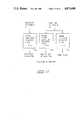
- FIG. 3 A block diagram of the decoder is shown in FIG. 3.
- the system is configured to perform in a pipelined manner where several messages are being processed simultaneously as depicted next:
- the received polynomial 32 is coupled to the syndrome generator 33.
- the syndrome generator 33 calculates each of the 2t syndromes for the given received polynomial 32.
- the syndrome generator 33 is coupled to the Euclid divide module 34.
- the Euclid divide module is coupled to the Euclid multiply module 35.
- the syndromes are input into the Euclid divide module 34.
- the Euclid divide module 34 generates the magnitude polynomial.
- a quotient developed by the Euclid divide module 34 is utilized by the Euclid multiply module 35 to develop the location polynomial.
- the Euclid divide module 34 and Euclid multiply module 35 are coupled to the polynomial solver 36.
- the magnitude polynomial and the location polynomial are input to the polynomial solver.
- the polynomial solver calculates the first derivative of the location polynomial.
- the polynomial solver 36 also finds the zeros of the location polynomial.
- the polynomial solver 36 is coupled to the inverse ROM 37 and to the error correction module 38.
- the inverse ROM 37 is programmed with the inverse, i.e., 1/x, for the elements of the particular Galois Field.
- the inverse ROM is used to find the inverse of the first derivative of the location polynomial.
- the polynomial solver 36 also supplies the magnitude polynomial and the location of the zeros of the location polynomial.
- the received polynomial 32 is also coupled to a FIFO RAM 39.
- the FIFO RAM 39 is sufficiently large to hold four received polynomials.
- the received polynomial is passed from the FIFO RAM 39 into the error correction unit 38 to be corrected by the magnitude and location information contained in the magnitude polynomial, location polynomial and the inverse of the first derivative of the location polynomial.
- the corrected polynomial 40 is output from the error correction decoder for use in another circuit.
- This error correction decoder operates in a four deep pipeline.
- the error correction module 38 can be acting upon a first message.
- the polynomial solver 36 can be acting upon a second message.
- the Euclid divide module 34 and the Euclid multiply module 35 operate upon a third message.
- the syndrome generator 33 can operate upon a fourth message.
- the FIFO RAM 39 stores the same four polynomials being acted upon as just described.
- the received polynomial, R(x), is input to both the FIFO for storage and to the syndrome calculator.
- the syndromes are passed to the Euclid Divide/Multiply module which generates ⁇ (x) and ⁇ (x).
- These polynomials are passed to Polynomial Solver.
- Real time decoding is achieved.
- the system clock being the symbol clock is a very important feature. Therefore, this decoder can decode symbols at the same time message symbols are presented. Decoders that cannot use the symbol clock as the system clock must utilize a more complex clock system where the decoder operates at a higher clock rate than the symbol clock. Therefore, for a given technology, this decoder can operate faster than other designs which require a system clock that operates at a higher rate than the symbol clock. Moreover, operating at a symbol clock rate reduces the amount of message buffering.
- the calculation of the syndromes is given in Eq. 1.
- the calculation r i ⁇ i (k+s) is evaluated for all r i and each k in (0, 1, 2, . . . 2t-1) and i in (0, 1, 2, . . . , n-1) (the number of input symbols in the message).
- the multiplier is a constant multiplier with the constant ⁇ k+s .
- a well known logic circuit for calculating syndrome Sk is shown in FIG. 6.
- Each of the ⁇ k+s is a zero of the generator polynomial G(x) of equation (2) or (3).
- each of the syndromes is the received polynomial evaluated at the zeros of the generator polynomial.
- the syndrome polynomials may be represented as: ##EQU12##
- n terms are multiplied by the appropriate constant representing a zero of the generator polynomial.
- n input R i symbols a total of n clock pulses are needed to calculated a syndrome. All 2t syndromes are calculated simultaneously with 2t circuits operating in parallel.
- FIG. 7 shows an improved circuit for use in generating syndromes.
- An input message symbol 42 is coupled into a Galois Field adder 43.
- the adder 43 is coupled to supply information to register 44.
- Register 44 is coupled to supply information to multiplier 45.
- the multiplier 45 is coupled to add information back into the adder 43.
- For an (n,k) code the first n-1 symbols are input to be recursively added and multiplied. As depicted in FIG. 7 these results reside in the register 44. After n-1 symbols are input, the last symbol is present at the input.
- the last clock pulse adds the last input symbol with the output of the multiplier 45 in the adder 43 and couples the result into the register 47. With the system clock being the symbol clock, if the contents of Syndrome are transferred to the shift register after n clock pulses (n input symbols), the contents of the shift register can be shifted out while the next set of syndromes are being calculated.
- the decoder be capable of decoding dual basis RS code words. It is necessary to transform the dual basis code words into regular field code words; this is accomplished by operating on each received word by T' as defined above and can be implemented with an array of XOR and ZERO cells as described above and shown in FIG. 1. An extra feature is added to the syndrome generator to operate in the regular field, the dual basis or any other basis.
- the Euclid divide/multiply module decomposes the 2t Syndrome polynomials into the error location polynomial ⁇ (x) and the error magnitude polynomial ⁇ (x).
- the relationship between the three polynomials is given in Eq. 8.
- the algorithm used to get ⁇ (x) and ⁇ (x) is the recursive application of the following 2 equations:
- q 1 (x) are the non-negative powers of the division ⁇ 1-2 (x) divided by ⁇ i-1 (x).
- the algorithm continues until the order of ⁇ i (x) is less than t.
- the circuitry for Eq. 10, the Euclid Divide module, consists of a linear array of 2t computational cells and a special cell to calculate the quotients.
- Each computational cell consists of a general multiplier/adder, two 8 wide registers, and two 8 wide 2 to 1 multiplexers.
- the circuitry for Eq. 11, the Euclid Multiply module, consists of a linear array of t+1 processors. Each processor consists of a general multiplier/adder, two 8 wide registers, and two 8 wide 2 to 1 multiplexers. This is the same circuitry used to implement the Euclid Divide Circuit. It is, however, connected differently.
- the Euclid Divide/Multiply engines may be implemented in a VLSI integrated circuit, with the Euclid divide engine roughly twice as big as the Euclid Multiply engine. Even though there are approximately 70,000 transistors in the device it may be implemented in a relatively small area.
- the extraordinary density is achievable because: (1) the general multiplier can be drawn exceedingly dense when domino logic design methodologies are employed, and (2) the given architecture is highly regular and requires virtually no interconnect. These two characteristics make it ideal for VLSI implementation.
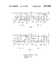
- FIGS. 8 and 9 The architecture of the hardware used to implement Euclid's algorithm is shown in FIGS. 8 and 9.
- FIG. 8 shows the Euclid divide hardware module
- FIG. 9 shows the Euclid multiply module.
- Each of the modules is designed to operate in one of two cycles.
- the Euclid divide module is comprised of 2t cells, 0 through 2t-1. Each of the cells 0 through 2t-2 is identical. Referring to cell 0, a typical cell each cell has an M i register 102, an M i-1 register 104, a multiplexer 106, a general Galois Field multiplier 108 and a Galois Field adder 110. Each of the registers M i and M i-1 are eight bit registers.
- the M i register 102 is coupled to receive an input.
- the output of the M i register is coupled to a first input of the multiplexer 106.
- the multiplexer 106 has a first input, a second input, a first output and a second output.
- the multiplexer may be configured in one of two ways as shown in FIG.
- the first configuration of the multiplexer passes a signal through from the first input to the first output and similarly from the second input to the second output.
- the second configuration of the multiplexer passes a signal from the first input to the second output and from the second input to the first output as shown in FIG. 8 cycle 2 for cell zero.
- the first output of the multiplexer 106 is coupled to a first input of the general multiplier 108 and as an input to the register M i-1 104.
- the output of the multiplier 108 is coupled to the first input of the adder 110.
- the second output of the multiplexer 106 is coupled to a second input of the adder 110.
- the output of the adder 110 is coupled to the input of the M i register of the next cell 112.
- the multiplier 108 is also coupled to receive the quotient Q(x) as a multiplicand on the second input.
- the M i register 102 is coupled to receive the output of AND gate 100. If a binary 1 is coupled to the load syndrome input of AND gate 100, the syndrome S(x) is coupled into the M i .sbsb.0 register 102. If the load syndrome input to AND gate 100 is set to 0 then a zero byte is coupled to the input of the M i .sbsb.0 register 102.
- the output of the M i register is coupled to the M(x) bus and to the inverse ROM 162.
- the inverse ROM is coupled to latch 160.
- the output of latch 160 is coupled to a second input of the Galois Field multiplier 158.
- the first output of the multiplexer 156 is also coupled to a first input of the Galois Field multiplier 158.
- the second output of the multiplexer 156 is coupled as an input to the M i-1 register 154.
- the difference between the hardware configuration in cycle 1 and cycle 2 is the configuration of the multiplexers.
- the multiplexers for cell zero through cell 2t-2 is configured as a straight pass through.
- the first input is coupled to the first output and the second input is coupled to the second output.
- the multiplexer 156 is configured to criss-cross the signal.
- the first input of multiplexer 156 is coupled to the second output of multiplexer 156 and the second input is coupled to the first output.
- each of the multiplexers is in the alternate state.
- cells zero through 2t-2 are coupled to criss-cross the signal and cell 2t-1 is coupled pass the signals straight through the multiplexer.
- the Euclid divide circuit is initialized by resetting all the M i-1 registers to zero except for cell 2t-1.
- M i-1 .sbsb.2t-1 is set to 00000001.
- the quotient bus is forced to zero.
- Each of the multiplexers for cell 0 though cell 2t-2 are in the data criss-cross mode.
- the multiplexer in cell 2t-1 is in the straight pass through mode.
- the load syndrome input to AND gate 100 is set to 1.
- the syndrome S(x) is shifted into each of the M i registers so the byte 2t of the syndrome is in register M i .sbsb.2t-1, the byte j+1 of the syndrome is in register M i .sbsb.j and the first byte of the syndrome is in register M i .sbsb.0.
- the first byte of the syndrome is transferred to M i .sbsb.0 by AND gate 100. Because the initialization sequence requires the multiplexer 106 to criss-cross the data the first byte of the syndrome enters the first input of multiplexer 106, exits the second output of multiplexer 106 and is coupled to the adder 110 as an addend.
- the output of the M i-1 .sbsb.0 register, which is zero, is criss-crossed through multiplexer 106 and is multiplied with a quotient bus of zero, which is also zero and added to the contents of the M i .sbsb.0 register in adder 110.
- the output of the adder is transferred to the M i .sbsb.1 register 112 in cell 1. In this way the contents of register M i .sbsb.0 are simply transferred to register M i .sbsb.1. This procedure is repeated 2t times in order to load the 2t bytes of the syndrome into the 2t M i registers.
- a cycle 2 is the same procedure to shift in the syndrome S(x) described above.
- An additional register which is not shown, counts the number of times the syndrome must be shifted before M i .sbsb.2t-1 is a non-zero byte. This can be done for example by incrementing a register. Once the contents of register M i .sbsb.2t-1 is non-zero then the core cycle is performed. After the core cycle the contents of the M i registers are shifted the same number of cycle 2 times as before the core cycle.
- the core cycle consists of a cycle 1 followed by a cycle 2.
- M i .sbsb.2t-1 contains the most significant byte of the ⁇ i-1 polynomial.
- the contents of M i .sbsb.2t-1 152 is stored in M i-1 .sbsb.2t-1 154. It is also input to the inverse ROM 162 which looks up the inverse, i.e., 1/M i .sbsb.2t-1 , passes that information through latch 160 and multiplies it by the contents of register M i-1 .sbsb.2t-1 and supplies that information to the quotient bus.
- the information on the quotient bus Q(x) is multiplied by the information in each of the remaining M i cells for example M i .sbsb.j-1 and added to M i-1 .sbsb.j-1 and stored as M i .sbsb.j.
- Register M i .sbsb.0 is loaded with all zeros.
- Core cycle 2 latches the inverse of M i .sbsb.2t-1 from cycle 1 in latch 160.
- Each M i-1 .sbsb.j-1 is multiplied by the quotient bus and the product is added to M i .sbsb.j-1 and stored in M i .sbsb.j.
- Cycle 2 is repeated for the number of pre-core cycle 2's.
- the value remaining in the last t bytes of the M i registers equals the polynomial ⁇ (x). This polynomial is shifted onto the M(x) line by performing cycles 2's. A new syndrome may be shifted in while shifting out ⁇ (x).
- the circuit is initialized as described above and the next ⁇ (x) polynomial is calculated.
- the highest order byte of the syndrome is shifted in first and the highest order byte of omega is shifted out first.
- the four Euclid divide equations: ##EQU13## are performed.
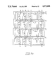
- the Euclid multiply algorithm is performed by the circuit shown in the block diagram of FIG. 9.
- Each of the t+1 cells, cells 0 through t are designed the same.
- cell t is comprised of a multiplexer 200, a Galois Field multiplier 202, a Galois Field adder 204, an L i register 206 and a L i-1 register 208.
- Each of the registers L i and L i-1 are 8 bit bytes.
- the multiplexer 200 is the same as the multiplexers in the Euclid divide circuit.
- the first input of the multiplexer 200 is coupled to receive the output of register L i .sbsb.t 206.
- the second input of multiplexer 200 is coupled to receive a zero.
- the first output of the multiplexer 200 is coupled to a first input of the adder 204.
- the second output of the multiplexer 200 is coupled to a first input of the multiplier 202 and to the input of register L i-1 .sbsb.t 208.
- the second input of multiplier 202 is coupled to receive the quotient bus Q(x) generated by the Euclid divide circuit described above.
- the output of the multiplier 202 is coupled to a second input of the adder 204.
- the output of the adder 204 is coupled into the register L i .sbsb.t 206.
- the second input of the multiplexer is coupled to the output of the preceding register L i-1 .sbsb.j.
- each multiplexer is configured to criss-cross the first input to the second output and the second input to the first output.
- all multiplexers are configured to pass the signal straight through from the first input to the first output and second input to the second output.
- each of the registers L i-1 .sbsb.j is set equal to zero by shifting in the zero applied to the second input of multiplexer 200 utilizing cycle 2s.
- cycle 1 the contents of L i are shifted to L i-1 .
- cell j the output of the L i .sbsb.j register 236 is coupled to the first input of the multiplexer 230.
- the multiplexer criss-crosses the data and so the information in the register L i .sbsb.j is supplied to the second output of the multiplexer 230.
- the multiplexer 230 is coupled to the input of the register L i-1 .sbsb.j 238.
- the information in register L i-1 j+1 228 is coupled to the second input of the multiplexer 230.
- the information in the register L i .sbsb.j 236 is coupled through the multiplexer 230 to a first input of the multiplier 232.
- the information on the quotient bus Q(x) from the Euclid divide circuit is multiplied by the information in the register L i .sbsb.j and applied to a second input of the adder 234. This information is added to the information in L i-1 .sbsb.j+1 and stored in register L i .sbsb.j 236.
- the only exception is cell t where the input to register L i-1 .sbsb.t equals zero.
- the control sequence for the Euclid multiply is the same as the control sequence for the Euclid divide with one exception.
- the stop control comes from the Euclid divide the contents of the L i registers are shifted into the L i-1 registers. This is done with a cycle 1 because the L i-1 registers can be easily shifted using cycle 2's and are thus used to pass the L(x) polynomial on for further processing.
- cell t contains the highest order of the L(x) polynomial. Any zero bytes are shifted out and discarded. Then the L(x) polynomial is shifted out, lowest order byte first. If the stop control comes on a cycle 1 there are no zeros to be shifted out otherwise if a stop control occurs on a cycle 2, which can only happen on a pre-core cycle 2, then the number of zeroes is the number of pre-core cycle 2's. A shift right control occurs with each post-core cycle in the Euclid divide algorithm.
- the circuit of FIG. 9 for the Euclid multiply module finds the error location polynomial by repeatedly applying the recursive equations: ##EQU14##
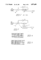
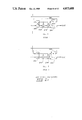
- Polynomial Solver evaluates three polynomials simultaneously: the error location polynomial ⁇ (x), error magnitude polynomial ⁇ (x), and the first derivative of the error location polynomial ⁇ '(x).
- the architecture of the Polynomial Solver consists of three registers stacks as shown in FIG. 11. One stack, the ⁇ (x) stack 50, searches for the zeros of the error location polynomial. An adjacent register stack, the ⁇ '(x) stack 52, evaluates the derivative of the error location polynomial. The ⁇ '(x) register stack shares the same input bus as error location, ⁇ (x), but only loads the odd coefficients of the location polynomial. The third register stack, the ⁇ (x) stack 54, receives the error magnitude polynomial from the Euclid module. The ⁇ (x) register stack 54 has a data path totally separate from the other two register stacks.
- the Polynomial Solver Since only n clock pulses are allowed to determine the zeros of ⁇ (x), there must be a separate control section to input the ⁇ (x) and ⁇ (x) coefficients from the Euclid module.
- the Polynomial Solver has shift registers that accept ⁇ (x) and ⁇ (x) asynchronously. In this mode. it is possible to receive the coefficients of ⁇ (x) for one message while at the same time searching for the zero's of the previous message. When the field elements of one error location polynomial have been completely searched, the coefficients from the ⁇ (x) previously loaded into the shift register can begin immediate evaluation and hence completing the required search in n clock pulses.
- the error magnitude and first derivative of the error location polynomials are evaluated at the same time and for the same field elements as the error location polynomial.
- a decoder has been presented that corrects up to 16 symbol errors for a Reed Solomon code at 80 Mbit/second data rate.
- the output consists of the corrected information symbols and a status word.
- the status word which is inserted in symbol location 31 (location of the first check symbol), contains the number of errors found and an uncorrectable error flag. If the message is uncorrectable, the information symbols are unchanged.
- the operation rate of the decoder chip set as a whole exceeds 1.65 BOPS.
Abstract
Description
C(x)=x.sup.2t ·M(x)+M(x)mod G(x). (1)
a(x)≡b(x) mod p(x).
              TABLE 1
______________________________________
α.sup.3
        α.sup.2
               α.sup.1
                      α.sup.0
                                 α.sup.3
                                      α.sup.2
                                           α.sup.1
                                                α.sup.0
______________________________________
α.sup.0
     0      0      0    1    α.sup.8
                                   0    1    0    1
α.sup.1
     0      0      1    0    α.sup.9
                                   1    0    1    0
α.sup.2
     0      1      0    0    α.sup.10
                                   0    1    1    1
α.sup.3
     1      0      0    0    α.sup.11
                                   1    1    1    0
α.sup.4
     0      0      1    1    α.sup.12
                                   1    1    1    1
α.sup.5
     0      1      1    0    α.sup.13
                                   1    1    0    1
α.sup.6
     1      1      0    0    α.sup.14
                                   1    0    0    1
α.sup.7
     1      0      1    1
______________________________________
R(x)=C(x)+E(x)=r.sub.N-1 x.sup.n-1 + . . . r.sub.1 x+r.sub.0
S(x)=R(x) mod G(x)
S(x)Λ(x)=Ω(x) mod x.sup.2t (6)
Ω(β.sup.i)/Λ'(β.sup.i)·(β.sup.111i) (7)
a(x)=a.sub.q-1 x.sup.q-1 +a.sub.q-2 x.sup.q-2 + . . . +a.sub.1 x.sup.1 +a.sub.0 x.sup.0
b(x)=b.sub.q-1 x.sup.q-1 +b.sub.q-2 x.sup.q-2 + . . . +b.sub.1 x.sup.1 +b.sub.0 x.sup.0
w(x)=γ(x) * β(x)+Θ(x)
x.sup.j β.sub.j mod p(x)
γ.sup.(1) (x)=γ(x)
Θ.sup.(1) (x)=Θ(x)+βoγ(x)
γ.sup.(i+1) (x)=xγ.sup.(i) (x) mod p(x)
Θ.sup.(i+1) (x)=xΘ.sup.(i) (x)+[βiγ(i+1)(x)] mod p(x)
γ.sup.(i+1) (x)=xγ.sup.(i) (x) mod p(x)
Θ.sup.(i+1) (x)=Θ.sup.(i) (x)+βiγ.sup.(i+1) (x)
Θ.sub.j.sup.(i+1) =γ.sub.j-1.sup.i +γ.sub.q-1.sup.i * p.sub.j
Θ.sub.j.sup.(i+1) =Θ.sub.j.sup.(i) +βiγ.sub.j.sup.(i+1)
R(x)=R.sub.0 x.sup.0 +R.sub.1 x.sup.1 +R.sub.2 x.sup.2 + . . . +R.sub.n-1 x.sup.n-1
Ω.sup.i (x)=Ω.sub.i-2 (x) mod Ω.sub.i-1 (x) (10)
Λ.sub.i (x)=-q.sub.i (x)Λ.sub.i-1 (x)+α.sub.i-2 (x) (11)
Claims (13)
Priority Applications (1)
| Application Number | Priority Date | Filing Date | Title |
|---|---|---|---|
| US07/105,401 US4873688A (en) | 1987-10-05 | 1987-10-05 | High-speed real-time Reed-Solomon decoder |
Applications Claiming Priority (1)
| Application Number | Priority Date | Filing Date | Title |
|---|---|---|---|
| US07/105,401 US4873688A (en) | 1987-10-05 | 1987-10-05 | High-speed real-time Reed-Solomon decoder |
Publications (1)
| Publication Number | Publication Date |
|---|---|
| US4873688A true US4873688A (en) | 1989-10-10 |
Family
ID=22305630
Family Applications (1)
| Application Number | Title | Priority Date | Filing Date |
|---|---|---|---|
| US07/105,401 Expired - Lifetime US4873688A (en) | 1987-10-05 | 1987-10-05 | High-speed real-time Reed-Solomon decoder |
Country Status (1)
| Country | Link |
|---|---|
| US (1) | US4873688A (en) |
Cited By (47)
| Publication number | Priority date | Publication date | Assignee | Title |
|---|---|---|---|---|
| US5099482A (en) * | 1989-08-30 | 1992-03-24 | Idaho Research Foundation, Inc. | Apparatus for detecting uncorrectable error patterns when using Euclid's algorithm to decode Reed-Solomon (BCH) codes |
| US5170399A (en) * | 1989-08-30 | 1992-12-08 | Idaho Research Foundation, Inc. | Reed-Solomon Euclid algorithm decoder having a process configurable Euclid stack |
| EP0545498A2 (en) * | 1991-12-04 | 1993-06-09 | Bts Broadcast Television Systems Gmbh | Method and circuit for decoding RS-coded data signals |
| WO1994001937A1 (en) * | 1992-07-09 | 1994-01-20 | Advanced Hardware Architectures, Incorporated | Single-stack implementation of a reed-solomon encoder/decoder |
| EP0595326A2 (en) * | 1992-10-30 | 1994-05-04 | Sony Corporation | Method of correcting lost data and circuit thereof |
| US5323402A (en) * | 1991-02-14 | 1994-06-21 | The Mitre Corporation | Programmable systolic BCH decoder |
| US5329535A (en) * | 1992-04-30 | 1994-07-12 | International Business Machines Corporation | Variable block lengths on-the-fly error correcting decoder |
| US5365529A (en) * | 1991-02-25 | 1994-11-15 | Bts Broadcast Television Systems Gmbh | Circuitry for detecting and correcting errors in data words occurring in Reed-Solomon coded blocks and determining when errors are uncorrectable by syndrome analysis, Euclid's algorithm and a Chien search |
| US5430739A (en) * | 1990-03-27 | 1995-07-04 | National Science Council | Real-time Reed-Solomon decoder |
| US5440570A (en) * | 1990-03-27 | 1995-08-08 | National Science Council | Real-time binary BCH decoder |
| US5517509A (en) * | 1993-03-31 | 1996-05-14 | Kabushiki Kaisha Toshiba | Decoder for decoding ECC using Euclid's algorithm |
| US5537426A (en) * | 1992-05-29 | 1996-07-16 | Goldstar Co., Ltd. | Operation apparatus for deriving erasure position Γ(x) and Forney syndrome T(x) polynomials of a Galois field employing a single multiplier |
| US5541937A (en) * | 1993-12-27 | 1996-07-30 | Canon Kabushiki Kaisha | Apparatus for uniformly correcting erasure and error of received word by using a common polynomial |
| GB2307572A (en) * | 1993-01-27 | 1997-05-28 | Nec Corp | Arithmetic circuit for producing an error numeric value polynomial and an error locator polynomial |
| US5642367A (en) * | 1994-02-07 | 1997-06-24 | Mitsubishi Semiconductor America, Inc. | Finite field polynomial processing module for error control coding |
| GB2274732B (en) * | 1993-01-27 | 1997-08-27 | Nec Corp | Arithmetic circuit having a simple structure for producing an error numeric value polynomial |
| US5689452A (en) * | 1994-10-31 | 1997-11-18 | University Of New Mexico | Method and apparatus for performing arithmetic in large galois field GF(2n) |
| US5715262A (en) * | 1995-07-12 | 1998-02-03 | Lsi Logic Corporation | Errors and erasures correcting reed-solomon decoder |
| EP0838905A2 (en) * | 1996-10-25 | 1998-04-29 | Matsushita Electric Industrial Co., Ltd. | Reed-Solomon Decoder |
| US5771244A (en) * | 1994-03-09 | 1998-06-23 | University Of Southern California | Universal Reed-Solomon coder/encoder |
| FR2769435A1 (en) * | 1997-08-30 | 1999-04-09 | Hyundai Electronics Ind | Synchronised Reed-Solomon decoder |
| US5898708A (en) * | 1994-06-16 | 1999-04-27 | Kabushiki Kaisha Toshiba | Error correction apparatus and method |
| US5970075A (en) * | 1997-06-18 | 1999-10-19 | Uniden San Diego Research And Development Center Inc. | Method and apparatus for generating an error location polynomial table |
| US5978950A (en) * | 1996-07-01 | 1999-11-02 | Daewoo Electronics Co., Ltd. | Polynomial evaluator for use in a reed-solomon decoder |
| US6133747A (en) * | 1997-07-22 | 2000-10-17 | University Of New Mexico | Time redundant radiation tolerant logic |
| WO2001039378A1 (en) * | 1999-11-24 | 2001-05-31 | Koninklijke Philips Electronics N.V. | Accelerated reed-solomon error correction |
| US6263471B1 (en) | 1999-03-05 | 2001-07-17 | Industrial Technology Research Institute | Method and apparatus for decoding an error correction code |
| US6378104B1 (en) * | 1996-10-30 | 2002-04-23 | Texas Instruments Incorporated | Reed-solomon coding device and method thereof |
| US6378103B1 (en) | 1998-05-19 | 2002-04-23 | Samsung Electronics Co., Ltd. | Apparatus and method for error correction in optical disk system |
| US6389442B1 (en) | 1997-12-30 | 2002-05-14 | Rsa Security Inc. | Efficient finite field multiplication in normal basis |
| US6473879B1 (en) * | 1989-07-13 | 2002-10-29 | Canon Kabushiki Kaisha | Encoding device and decoding device suitable for dubbing |
| US20030068037A1 (en) * | 2001-10-10 | 2003-04-10 | Stmicroelectronics S.R.I. | Circuit for the inner or scalar product computation in galois fields |
| US6583470B1 (en) | 1999-03-09 | 2003-06-24 | Science & Technology Corporation @ Unm | Radiation tolerant back biased CMOS VLSI |
| US20030126543A1 (en) * | 2001-11-28 | 2003-07-03 | Chen-Yi Lee | Method and apparatus for solving key equation polynomials in decoding error correction codes |
| US6694476B1 (en) | 2000-06-02 | 2004-02-17 | Vitesse Semiconductor Corporation | Reed-solomon encoder and decoder |
| US6738942B1 (en) | 2000-06-02 | 2004-05-18 | Vitesse Semiconductor Corporation | Product code based forward error correction system |
| US20050149821A1 (en) * | 2003-12-18 | 2005-07-07 | Hoon Lee | Apparatus for FEC supporting transmission of variable-length frames in TDMA system and method of using the same |
| US6920182B2 (en) | 2001-01-09 | 2005-07-19 | Microtune (Texas), L.P. | Delta-sigma modulator system and method |
| US6983414B1 (en) | 2001-03-30 | 2006-01-03 | Cisco Technology, Inc. | Error insertion circuit for SONET forward error correction |
| US7003715B1 (en) | 2001-03-30 | 2006-02-21 | Cisco Technology, Inc. | Galois field multiply accumulator |
| US7124064B1 (en) | 2001-03-30 | 2006-10-17 | Cisco Technology, Inc. | Automatic generation of hardware description language code for complex polynomial functions |
| US20080016432A1 (en) * | 2006-07-12 | 2008-01-17 | Peter Lablans | Error Correction in Multi-Valued (p,k) Codes |
| US7447982B1 (en) * | 2001-03-30 | 2008-11-04 | Cisco Technology, Inc. | BCH forward error correction decoder |
| US20090172501A1 (en) * | 2006-03-03 | 2009-07-02 | Ternarylogic Llc | Multi-State Symbol Error Correction in Matrix Based Codes |
| US20100161701A1 (en) * | 2008-12-18 | 2010-06-24 | Microsoft Corporation | Polynomial representation for symbolic computation |
| US8296632B1 (en) * | 2008-06-06 | 2012-10-23 | Mohammad Amin Shokrollahi | Encoding and decoding of generalized Reed-Solomon codes using parallel processing techniques |
| US20150022384A1 (en) * | 2012-09-05 | 2015-01-22 | Q-Analog Corporation | System Clock Jitter Correction |
Citations (4)
| Publication number | Priority date | Publication date | Assignee | Title |
|---|---|---|---|---|
| US4162480A (en) * | 1977-01-28 | 1979-07-24 | Cyclotomics, Inc. | Galois field computer |
| US4413339A (en) * | 1981-06-24 | 1983-11-01 | Digital Equipment Corporation | Multiple error detecting and correcting system employing Reed-Solomon codes |
| US4434487A (en) * | 1981-10-05 | 1984-02-28 | Digital Equipment Corporation | Disk format for secondary storage system |
| US4564945A (en) * | 1983-06-20 | 1986-01-14 | Reference Technology, Inc. | Error-correction code for digital data on video disc |
-
1987
- 1987-10-05 US US07/105,401 patent/US4873688A/en not_active Expired - Lifetime
Patent Citations (4)
| Publication number | Priority date | Publication date | Assignee | Title |
|---|---|---|---|---|
| US4162480A (en) * | 1977-01-28 | 1979-07-24 | Cyclotomics, Inc. | Galois field computer |
| US4413339A (en) * | 1981-06-24 | 1983-11-01 | Digital Equipment Corporation | Multiple error detecting and correcting system employing Reed-Solomon codes |
| US4434487A (en) * | 1981-10-05 | 1984-02-28 | Digital Equipment Corporation | Disk format for secondary storage system |
| US4564945A (en) * | 1983-06-20 | 1986-01-14 | Reference Technology, Inc. | Error-correction code for digital data on video disc |
Non-Patent Citations (6)
| Title |
|---|
| "Error-Correction Coding for Digital Communications" by George C. Clark, Jr. and J. Bibb Cain, pp. 195-201, published by Plenum Press, New York, First Printing Jun. 1981. |
| "VLSI Reed Solomon Decoder Design" by Gary K. Maki, Patrick A. Owsley, Kelley B, Cameron and Jack Venbrux, published in Communications-Computers: Teamed for the '90's, Conference Record vol. 3 of 3, 1986 IEEE Military Communications Conference. |
| Berlekamp, Algebraic Coding Theory, McGraw Hill Book Co., 1968, pp. 21 30. * |
| Berlekamp, Algebraic Coding Theory, McGraw-Hill Book Co., 1968, pp. 21-30. |
| Error Correction Coding for Digital Communications by George C. Clark, Jr. and J. Bibb Cain, pp. 195 201, published by Plenum Press, New York, First Printing Jun. 1981. * |
| VLSI Reed Solomon Decoder Design by Gary K. Maki, Patrick A. Owsley, Kelley B, Cameron and Jack Venbrux, published in Communications Computers: Teamed for the 90 s, Conference Record vol. 3 of 3, 1986 IEEE Military Communications Conference. * |
Cited By (64)
| Publication number | Priority date | Publication date | Assignee | Title |
|---|---|---|---|---|
| US6473879B1 (en) * | 1989-07-13 | 2002-10-29 | Canon Kabushiki Kaisha | Encoding device and decoding device suitable for dubbing |
| US5170399A (en) * | 1989-08-30 | 1992-12-08 | Idaho Research Foundation, Inc. | Reed-Solomon Euclid algorithm decoder having a process configurable Euclid stack |
| US5099482A (en) * | 1989-08-30 | 1992-03-24 | Idaho Research Foundation, Inc. | Apparatus for detecting uncorrectable error patterns when using Euclid's algorithm to decode Reed-Solomon (BCH) codes |
| US5430739A (en) * | 1990-03-27 | 1995-07-04 | National Science Council | Real-time Reed-Solomon decoder |
| US5440570A (en) * | 1990-03-27 | 1995-08-08 | National Science Council | Real-time binary BCH decoder |
| US5323402A (en) * | 1991-02-14 | 1994-06-21 | The Mitre Corporation | Programmable systolic BCH decoder |
| US5365529A (en) * | 1991-02-25 | 1994-11-15 | Bts Broadcast Television Systems Gmbh | Circuitry for detecting and correcting errors in data words occurring in Reed-Solomon coded blocks and determining when errors are uncorrectable by syndrome analysis, Euclid's algorithm and a Chien search |
| US5490154A (en) * | 1991-12-04 | 1996-02-06 | U.S. Philips Corporation | Method of and circuit arrangement for decoding RS-coded data signals |
| EP0545498A2 (en) * | 1991-12-04 | 1993-06-09 | Bts Broadcast Television Systems Gmbh | Method and circuit for decoding RS-coded data signals |
| EP0545498A3 (en) * | 1991-12-04 | 1994-02-23 | Broadcast Television Syst | |
| US5329535A (en) * | 1992-04-30 | 1994-07-12 | International Business Machines Corporation | Variable block lengths on-the-fly error correcting decoder |
| US5537426A (en) * | 1992-05-29 | 1996-07-16 | Goldstar Co., Ltd. | Operation apparatus for deriving erasure position Γ(x) and Forney syndrome T(x) polynomials of a Galois field employing a single multiplier |
| WO1994001937A1 (en) * | 1992-07-09 | 1994-01-20 | Advanced Hardware Architectures, Incorporated | Single-stack implementation of a reed-solomon encoder/decoder |
| EP0595326A3 (en) * | 1992-10-30 | 1995-10-04 | Sony Corp | Method of correcting lost data and circuit thereof |
| EP0989680A1 (en) * | 1992-10-30 | 2000-03-29 | Sony Corporation | Method of correcting lost data and circuit thereof |
| EP0989679A1 (en) * | 1992-10-30 | 2000-03-29 | Sony Corporation | Method of correcting lost data and circuit thereof |
| EP0991196A1 (en) * | 1992-10-30 | 2000-04-05 | Sony Corporation | Method of correcting lost data and circuit thereof |
| US5566190A (en) * | 1992-10-30 | 1996-10-15 | Sony Corporation | Apparatus and methods for correcting lost data |
| EP0595326A2 (en) * | 1992-10-30 | 1994-05-04 | Sony Corporation | Method of correcting lost data and circuit thereof |
| GB2307572B (en) * | 1993-01-27 | 1997-08-27 | Nec Corp | Arithmetic circuit having a simple structure for producing an error locator coefficient of an error locator polynomial |
| GB2274732B (en) * | 1993-01-27 | 1997-08-27 | Nec Corp | Arithmetic circuit having a simple structure for producing an error numeric value polynomial |
| GB2307572A (en) * | 1993-01-27 | 1997-05-28 | Nec Corp | Arithmetic circuit for producing an error numeric value polynomial and an error locator polynomial |
| US5517509A (en) * | 1993-03-31 | 1996-05-14 | Kabushiki Kaisha Toshiba | Decoder for decoding ECC using Euclid's algorithm |
| US5541937A (en) * | 1993-12-27 | 1996-07-30 | Canon Kabushiki Kaisha | Apparatus for uniformly correcting erasure and error of received word by using a common polynomial |
| US5642367A (en) * | 1994-02-07 | 1997-06-24 | Mitsubishi Semiconductor America, Inc. | Finite field polynomial processing module for error control coding |
| US5771244A (en) * | 1994-03-09 | 1998-06-23 | University Of Southern California | Universal Reed-Solomon coder/encoder |
| US5898708A (en) * | 1994-06-16 | 1999-04-27 | Kabushiki Kaisha Toshiba | Error correction apparatus and method |
| US5689452A (en) * | 1994-10-31 | 1997-11-18 | University Of New Mexico | Method and apparatus for performing arithmetic in large galois field GF(2n) |
| US5715262A (en) * | 1995-07-12 | 1998-02-03 | Lsi Logic Corporation | Errors and erasures correcting reed-solomon decoder |
| US5978950A (en) * | 1996-07-01 | 1999-11-02 | Daewoo Electronics Co., Ltd. | Polynomial evaluator for use in a reed-solomon decoder |
| EP0838905A3 (en) * | 1996-10-25 | 2001-03-21 | Matsushita Electric Industrial Co., Ltd. | Reed-Solomon decoder |
| EP1370004A3 (en) * | 1996-10-25 | 2005-05-04 | Matsushita Electric Industrial Co., Ltd. | Arithmetic unit for Reed-Solomon decoder |
| EP0838905A2 (en) * | 1996-10-25 | 1998-04-29 | Matsushita Electric Industrial Co., Ltd. | Reed-Solomon Decoder |
| US6378104B1 (en) * | 1996-10-30 | 2002-04-23 | Texas Instruments Incorporated | Reed-solomon coding device and method thereof |
| US5970075A (en) * | 1997-06-18 | 1999-10-19 | Uniden San Diego Research And Development Center Inc. | Method and apparatus for generating an error location polynomial table |
| US6133747A (en) * | 1997-07-22 | 2000-10-17 | University Of New Mexico | Time redundant radiation tolerant logic |
| FR2769435A1 (en) * | 1997-08-30 | 1999-04-09 | Hyundai Electronics Ind | Synchronised Reed-Solomon decoder |
| US6389442B1 (en) | 1997-12-30 | 2002-05-14 | Rsa Security Inc. | Efficient finite field multiplication in normal basis |
| US6378103B1 (en) | 1998-05-19 | 2002-04-23 | Samsung Electronics Co., Ltd. | Apparatus and method for error correction in optical disk system |
| US6263471B1 (en) | 1999-03-05 | 2001-07-17 | Industrial Technology Research Institute | Method and apparatus for decoding an error correction code |
| US6583470B1 (en) | 1999-03-09 | 2003-06-24 | Science & Technology Corporation @ Unm | Radiation tolerant back biased CMOS VLSI |
| US6539515B1 (en) * | 1999-11-24 | 2003-03-25 | Koninklijke Philips Electronics N.V. | Accelerated Reed-Solomon error correction |
| WO2001039378A1 (en) * | 1999-11-24 | 2001-05-31 | Koninklijke Philips Electronics N.V. | Accelerated reed-solomon error correction |
| US6694476B1 (en) | 2000-06-02 | 2004-02-17 | Vitesse Semiconductor Corporation | Reed-solomon encoder and decoder |
| US6738942B1 (en) | 2000-06-02 | 2004-05-18 | Vitesse Semiconductor Corporation | Product code based forward error correction system |
| US6810499B2 (en) | 2000-06-02 | 2004-10-26 | Vitesse Semiconductor Corporation | Product code based forward error correction system |
| US6920182B2 (en) | 2001-01-09 | 2005-07-19 | Microtune (Texas), L.P. | Delta-sigma modulator system and method |
| US7124064B1 (en) | 2001-03-30 | 2006-10-17 | Cisco Technology, Inc. | Automatic generation of hardware description language code for complex polynomial functions |
| US6983414B1 (en) | 2001-03-30 | 2006-01-03 | Cisco Technology, Inc. | Error insertion circuit for SONET forward error correction |
| US7003715B1 (en) | 2001-03-30 | 2006-02-21 | Cisco Technology, Inc. | Galois field multiply accumulator |
| US7447982B1 (en) * | 2001-03-30 | 2008-11-04 | Cisco Technology, Inc. | BCH forward error correction decoder |
| US20030068037A1 (en) * | 2001-10-10 | 2003-04-10 | Stmicroelectronics S.R.I. | Circuit for the inner or scalar product computation in galois fields |
| US7206410B2 (en) * | 2001-10-10 | 2007-04-17 | Stmicroelectronics S.R.L. | Circuit for the inner or scalar product computation in Galois fields |
| US20030126543A1 (en) * | 2001-11-28 | 2003-07-03 | Chen-Yi Lee | Method and apparatus for solving key equation polynomials in decoding error correction codes |
| US20050149821A1 (en) * | 2003-12-18 | 2005-07-07 | Hoon Lee | Apparatus for FEC supporting transmission of variable-length frames in TDMA system and method of using the same |
| US7581155B2 (en) * | 2003-12-18 | 2009-08-25 | Electronics And Telecommunications Research Institute | Apparatus for FEC supporting transmission of variable-length frames in TDMA system and method of using the same |
| US20090172501A1 (en) * | 2006-03-03 | 2009-07-02 | Ternarylogic Llc | Multi-State Symbol Error Correction in Matrix Based Codes |
| US8832523B2 (en) * | 2006-03-03 | 2014-09-09 | Ternarylogic Llc | Multi-state symbol error correction in matrix based codes |
| US20080016432A1 (en) * | 2006-07-12 | 2008-01-17 | Peter Lablans | Error Correction in Multi-Valued (p,k) Codes |
| US9203436B2 (en) * | 2006-07-12 | 2015-12-01 | Ternarylogic Llc | Error correction in multi-valued (p,k) codes |
| US8296632B1 (en) * | 2008-06-06 | 2012-10-23 | Mohammad Amin Shokrollahi | Encoding and decoding of generalized Reed-Solomon codes using parallel processing techniques |
| US20100161701A1 (en) * | 2008-12-18 | 2010-06-24 | Microsoft Corporation | Polynomial representation for symbolic computation |
| US20150022384A1 (en) * | 2012-09-05 | 2015-01-22 | Q-Analog Corporation | System Clock Jitter Correction |
| US8957796B2 (en) * | 2012-09-05 | 2015-02-17 | IQ—Analog Corporation | System clock jitter correction |
Similar Documents
| Publication | Publication Date | Title |
|---|---|---|
| US4873688A (en) | High-speed real-time Reed-Solomon decoder | |
| US4868828A (en) | Architecture for time or transform domain decoding of reed-solomon codes | |
| US5715262A (en) | Errors and erasures correcting reed-solomon decoder | |
| EP0114938B1 (en) | On-the-fly multibyte error correction | |
| US6637002B1 (en) | Decoder for error correcting block codes | |
| US5517509A (en) | Decoder for decoding ECC using Euclid's algorithm | |
| US7502989B2 (en) | Even-load software Reed-Solomon decoder | |
| US20030192007A1 (en) | Code-programmable field-programmable architecturally-systolic Reed-Solomon BCH error correction decoder integrated circuit and error correction decoding method | |
| EP0838905B1 (en) | Reed-Solomon Decoder | |
| US6119262A (en) | Method and apparatus for solving key equation polynomials in decoding error correction codes | |
| US6571368B1 (en) | Systolic Reed-Solomon decoder | |
| US5535225A (en) | Time domain algebraic encoder/decoder | |
| US7089276B2 (en) | Modular Galois-field subfield-power integrated inverter-multiplier circuit for Galois-field division over GF(256) | |
| US7162679B2 (en) | Methods and apparatus for coding and decoding data using Reed-Solomon codes | |
| US7870468B1 (en) | Reed-solomon decoder using a configurable arithmetic processor | |
| KR100260415B1 (en) | High speed serial error position polynomual calculation circuit | |
| US6263471B1 (en) | Method and apparatus for decoding an error correction code | |
| US20040078747A1 (en) | Generalized forney algorithm circuit | |
| US6735737B2 (en) | Error correction structures and methods | |
| US20030159103A1 (en) | Efficient method for fast decoding of BCH binary codes | |
| Maki et al. | VLSI Reed Solomon decoder design | |
| US20180006664A1 (en) | Methods and apparatus for performing reed-solomon encoding by lagrangian polynomial fitting | |
| US20070011592A1 (en) | Decoder architecture for Reed Solomon codes | |
| EP0793352B1 (en) | Apparatus for determining the error evaluator polynomial for use in a Reed-Solomon decoder | |
| Khan et al. | Hardware implementation of shortened (48, 38) Reed Solomon forward error correcting code |
Legal Events
| Date | Code | Title | Description |
|---|---|---|---|
| AS | Assignment |
Owner name: IDAHO RESEARCH FOUNDATION, A CORP. OF IDAHO Free format text: ASSIGNMENT OF ASSIGNORS INTEREST.;ASSIGNORS:MAKI, GARY K.;CAMERON, KELLY;OWSLEY, PATRICK A.;REEL/FRAME:004897/0785 Effective date: 19880204 |
|
| STCF | Information on status: patent grant |
Free format text: PATENTED CASE |
|
| AS | Assignment |
Owner name: BOARD OF REGENTS OF THE UNIVERSITY OF IDAHO, IDAHO Free format text: SECURITY INTEREST;ASSIGNOR:IDAHO RESEARCH FOUNDATION, INC.;REEL/FRAME:005368/0648 Effective date: 19900216 |
|
| AS | Assignment |
Owner name: TRANSCO SYNDICATE #1, LTD., CALIFORNIA Free format text: SECURITY INTEREST;ASSIGNOR:ADVANCED HARDWARE ARCHITECTURES, INC., A CORP OF DE;REEL/FRAME:005404/0393 Effective date: 19900703 |
|
| CC | Certificate of correction | ||
| FPAY | Fee payment |
Year of fee payment: 4 |
|
| FPAY | Fee payment |
Year of fee payment: 8 |
|
| FPAY | Fee payment |
Year of fee payment: 12 |