EP0247650A2 - Motorgeschwindigkeitsregelsystem - Google Patents
Motorgeschwindigkeitsregelsystem Download PDFInfo
- Publication number
- EP0247650A2 EP0247650A2 EP19870200769 EP87200769A EP0247650A2 EP 0247650 A2 EP0247650 A2 EP 0247650A2 EP 19870200769 EP19870200769 EP 19870200769 EP 87200769 A EP87200769 A EP 87200769A EP 0247650 A2 EP0247650 A2 EP 0247650A2
- Authority
- EP
- European Patent Office
- Prior art keywords
- output
- signal
- interrupt
- detector
- counter
- Prior art date
- Legal status (The legal status is an assumption and is not a legal conclusion. Google has not performed a legal analysis and makes no representation as to the accuracy of the status listed.)
- Granted
Links
Images


Classifications
-
- H—ELECTRICITY
- H02—GENERATION; CONVERSION OR DISTRIBUTION OF ELECTRIC POWER
- H02P—CONTROL OR REGULATION OF ELECTRIC MOTORS, ELECTRIC GENERATORS OR DYNAMO-ELECTRIC CONVERTERS; CONTROLLING TRANSFORMERS, REACTORS OR CHOKE COILS
- H02P25/00—Arrangements or methods for the control of AC motors characterised by the kind of AC motor or by structural details
- H02P25/02—Arrangements or methods for the control of AC motors characterised by the kind of AC motor or by structural details characterised by the kind of motor
- H02P25/10—Commutator motors, e.g. repulsion motors
- H02P25/14—Universal motors
- H02P25/145—Universal motors whereby the speed is regulated by measuring the motor speed and comparing it with a given physical value, speed feedback
-
- H—ELECTRICITY
- H02—GENERATION; CONVERSION OR DISTRIBUTION OF ELECTRIC POWER
- H02P—CONTROL OR REGULATION OF ELECTRIC MOTORS, ELECTRIC GENERATORS OR DYNAMO-ELECTRIC CONVERTERS; CONTROLLING TRANSFORMERS, REACTORS OR CHOKE COILS
- H02P23/00—Arrangements or methods for the control of AC motors characterised by a control method other than vector control
- H02P23/0077—Characterised by the use of a particular software algorithm
-
- Y—GENERAL TAGGING OF NEW TECHNOLOGICAL DEVELOPMENTS; GENERAL TAGGING OF CROSS-SECTIONAL TECHNOLOGIES SPANNING OVER SEVERAL SECTIONS OF THE IPC; TECHNICAL SUBJECTS COVERED BY FORMER USPC CROSS-REFERENCE ART COLLECTIONS [XRACs] AND DIGESTS
- Y10—TECHNICAL SUBJECTS COVERED BY FORMER USPC
- Y10S—TECHNICAL SUBJECTS COVERED BY FORMER USPC CROSS-REFERENCE ART COLLECTIONS [XRACs] AND DIGESTS
- Y10S388/00—Electricity: motor control systems
- Y10S388/907—Specific control circuit element or device
- Y10S388/912—Pulse or frequency counter
Definitions
- This invention relates to a speed control system for an a.c. electric motor which is connected in series with a controllable switch between first and second a.c. supply conductors, which system comprises a data processing system comprising a program store and a digital data processor for performing a program of processing operations on digital data in accordance with program data contained in said program store, which processing system has an output coupled to a control input of said switch, a detector for zero potential between said supply conductors, which detector has an input coupled to said supply conductors and an output coupled to an input of said data processing system, for generating an output signal when zero potential occurs between said supply conductors, a tachogenerator having an input coupled to said motor and an output coupled to an interrupt signal input of said data processing system, and a counter having an input coupled to an output of a clock signal source and an output coupled to an interrupt signal input of said data processing system, for generating an output signal when the count therein reaches a predetermined value, said program comprising a cyclic main program and first and
- the invention provides a speed control system for an a.c. electric motor which is connected in series with a controllable switch between first and second a.c. supply conductors, which system comprises a data processing system comprising a program store and a digital data processor for performing a program of processing operations on digital data in accordance with program data contained in said program store, which processing system has an output coupled to a control input of said switch, a detector for zero potential between said supply conductors, which detector has an input coupled to said supply conductors and an output coupled to an input of said data processing system, for generating an output signal when zero potential occurs between said supply conductors, a tachogenerator having an input coupled to said motor and an output coupled to an interrupt signal input of said data processing system, and a counter having an input coupled to an output of a clock signal source and an output coupled to an interrupt signal input of said data processing system, for generating an output signal when the count therein reaches a predetermined value, said program comprising a cyclic main program and first and
- the fourth storage means each for a digital representation of a respective time which has elapsed between the generation of an output signal by the detector and the subsequent generation of an output signal by the tachogenerator, or for information from which this time can be calculated
- the said third interrupt routine comprising the steps of (a) loading the counter with a value such that the count therein will next reach said predetermined value when the switch is required to conduct, which loading value is derived from the first storage means, and (b) updating the contents of the second storage means
- the said second interrupt routine comprising the step of (c) generating at the said output of the processing system a conduct control signal for the switch
- the said first interrupt routine comprising, at least some times it is performed, the steps of (d) reading the contents of the counter and storing in one of the third and fourth storage means a digital representation, derived from the contents thus read and the value with which the counter was loaded when the immediately preceding output signal was generated by the detector, of the time which has elapsed since the generation of an output signal by the detector,
- Some single-chip microcomputers e.g. those of the MAB8400 family available from Mullard Ltd., U.K. have a single counter/timer on-chip, this being clocked by the source which also controls the actual microcomputer, and generating an interrupt each time it overflows. Such overflows normally occur several times during each half-cycle of the a.c. public electricity supply.
- the aforesaid counter may comprise a first portion which is arranged to generate a signal at an output thereof each time this portion overflows, which output constitutes the output of the counter which is coupled to an interrupt signal input of the data processing system, and a second portion constituted by further storage means for a digital representation of the number of output signals which have been generated by overflow of the first portion since the last output signal generated by the detector occurred, the digital representation stored by the first storage means may be arranged to be in terms of a whole number of complete cycle periods of said first portion plus a fraction of a second complete cycle period, step (a) may comprise loading the first portion with a value such that it will next overflow after a period of time equal to the said fraction of a complete cycle period and resetting the content of the further storage means, and the second interrupt routine may constitute a branch of a larger interrupt routine which is arranged to be performed in response to each overflow of the said first portion,
- a speed control system for an a.c. electric motor 1 which is connected in series with a :ontrollable switch 2 in the form of a triac between irst and second a.c. supply conductors 3 and 4 :omprises a data processing system 5.
- System 5 ncludes a single-chip microcomputer 6 which in :onventional manner comprises a program store 7 and a digital data processor 8 for performing a program of processing operations on digital data in accordance with program data contained in the store 7. This program will be described more fully below.
- Microcomputer 6 is, in the present example, a member of the MAB 8400 family available from Mullard Ltd., U.K., and in consequence has but a single interrupt signal input j NT /TO. Only those connections between microcomputer 6 and the exterior which are particularly relevant to the following description are shown.
- the microcomputer 6 includes internally first, second, third, fourth and fifth storage means in the form of registers FAR, ZCSLTA, TISLTA, NTT and LTT respectively, further storage means in the form of registers ZCSLTA*, CTPLV, TIBF, PM * , PT and PMrespec- tively, and an 8-bit timer/counter CT which is driven by an internal clock CL the frequency of which is determined by an external crystal resonator 12 connected between pins XTAL 1 and XTAL 2 of the microcomputer 6.
- the clock CL also controls the overall operation of the microcomputer, with the result that counter CT is clocked once every machine cycle performed by the microcomputer. Each time the content of counter CT corresponds to its maximum count and receives a further clock pulse, i.e. overflows, it resets and generates an internal interrupt signal.
- Control of the speed of the motor 1 is effected by controlling the firing angle of triac 2, i.e. the instant in each half-cycle of the a.c. supply fed to the conductors 3 and 4 at which the triac 2 is fired, these instants being made earlier in the half cycles (corresponding to a larger firing angle) if the actual motor speed is less than a target speed a digital representation of which is stored in the register PT in microcomputer 6, and being made later in the half-cycles (corresponding to a smaller firing angle) if the actual speed is greater than the target speed.
- the trigger pulses for the triac 2 are generated by microcomputer 6 at the correct instants at a pair of parallel-connected output port pins P010 and P011 and are fed to the triac gate via an amplifier 9.
- the microcomputer 6 needs information about when each zero crossing occurs in the supply fed to the conductors 3 and 4, i.e. when each half-cycle starts, and also about the actual speed of the motor 1.
- the system 5 also includes first and second interrupt signal sources in the form of a detector 10 for zero potential between the conductors 3 and 4, and a tachogenerator 11 driven by the motor 1.
- Source 10 In the quiescent state each of these sources produces logic "1" " at its output, source 10 producing a logic "0" pulse each time the voltage between conductors 3 and 4 reaches zero and source 11 producing logic "0" pulses at a rate which is directly proportional to the speed of the motor 1.
- Source 10 may comprise a pair of voltage comparators for detecting the presence on one of the conductors 3 and 4 of a potential less than a very small positive and negative potential respectively relative to the other, the outputs of which comparators are combined by means of a NAND function).
- Each of these logic "0" pulses initiates an interrupt routine in the microcomputer 6, this routine comprising first and second branches, the first being taken in response to a logic "0" pulse from zero crossing detector 10 and the second being taken in response to a logic "0" pulse from tachogenerator 11.
- the outputs 13 and 14 of the sources 10 and 11 are coupled to respective inputs 15 and 16 of a OR-function circuit 17 the output 18 of which is connected to the interrupt signal input INT/TO of microcomputer 6.
- the coupling from output 13 to input 15 is via the set input 19 and the output 20 of a bistable device 21, and the coupling from output 14 to input 16 is via the set input 22 and the output 23 of a bistable device 24.
- Device 21 comprises in known manner two cross-coupled NAND-gates 25 and 26, and device 24 similarly comprises two cross-coupled NAND-gates 27 and 28.
- OR-function circuit 17 also has an override signal input 29 to which is connected a further output port pin P016 of microcomputer 6.
- Two further output port pins P06 and P07 of microcomputer 6 are connected to reset inputs 31 and 32 respectively of bistable devices 21 and 24 respectively.
- the output 20 of bistable device 21 is also connected to a test input pin T1 of microcomputer 6.
- the bistable devices 21 and 24 and the disable input 29 of OR-function circuit 17 are provided for the following reason.
- Microcomputer 6 responds, at its interrupt signal input ⁇ NT /TO, only to a signal transition from logic "1 " to logic "0", and not to the mere presence thereat of logic "0". Because the logic "0" pulses from tachogenerator 11 can occur at any time during a cycle of the voltage supply fed to conductors 3 and 4 it is very possible that, at least occasionally, one of these will overlap a logic "0" pulse from zero-crossing detector 10.
- Output pin P016 is normally logic "1", this output pin being connected to one input of a NAND-gate 34 forming part of circuit 17.
- the other input of NAND-gate 34 is fed from the outputs 20 and 23 of devices 21 and 24 via a NAND-gate 35 also forming part of circuit 17, so that if it is assumed that both devices initially produce a logic "1” a a logic “0” subsequently produced by either of these devices (in response to a logic "0" pulse produced by the source 10 or the source 11) will result in the application of a signal transition from logic "1" to logic "0” to the interrupt signal input I NT /TO, and hence in the carrying out of an interrupt routine by microcomputer 6.
- This interrupt routine includes the following steps.
- bistable device 21 is in the set state, indicating that zero-crossing detector 10 has produced a logic "0" pulse, and a first branch of the interrupt routine is taken. If the signal state at test input T1 is logic "1" " on the other hand, then tachogenerator 11 must have produced the logic "0" pulse which gave rise to the interrupt, and a second branch of the interrupt routine is taken in this case.
- microcomputer 6 At the end of the first branch microcomputer 6 generates a logic "0" pulse at its output P06, resetting bistable device 21, and also generates a logic "0" pulse at its output P016.
- microcomputer 6 At the end of the second branch microcomputer 6 generates a logic "0" pulse at its output P07, resetting bistable device 24, and also generates a logic "0" pulse at its output P016. If only one of these bistable devices is in the set state when the reset occurs (because only one of the sources 10 and 11 has produced a logic "0" pulse) the signal level at interrupt signal input ) NT* /TO merely returns to logic “1" and remains there until one of the bistable devices 21 and 24 again assumes the set state.
- test pin T1 is connected to the output of bistable device 21, if both the tachogenerator 11 and the mains zero crossing detector 10 produce a logic "0" pulse substantially simultaneously the interrupt routine branch corresponding to the zero-crossing detector 10 will be performed before the branch corresponding to the tachogenerator 11.
- An alternative possibility is to connect the output 23 of device 24 to a further test input of microcomputer 6, for example another pin of the port PO, and to arrange that this and pin T1 are tested in the required order at the beginning of the interrupt routine. This would be necessary in any case if one or more further interrupt signal sources and associated bistable devices were provided connected to further respective inputs of NAND-gate 35, as it will be evident is possible. If such a further source and associated device is present microcomputer 6 will obviously have to be provided with a corresponding further output similar to P06 and P07 connected to the reset input of the further bistable device.
- Fig. 1 operates as follows, it being assumed, for example, that crystal resonator 12 is chosen to resonate at such a frequency that counter CT is clocked at a frequency such that there are between five and seven complete fill (cycle) periods for this counter in each half-cycle of the a.c. voltage applied to conductors 3 and 4.
- Program store 7 contains a cyclic main program which basically consists of a calculation routine for calculating the actual speed of the motor 1 as indicated by the period of the output pulses of the tachogenerator 11 and, from this and the target speed indicated by the content of the register PT, the firing angle for the triac 2 required in each half-cycle of the a.c. supply fed to the conductors 3 and 4.
- This calculation results in an eleven-bit digital number indicating the number of counts which counter CT should make after each zero crossing occurs in the a.c. supply before the triac is fired, which number is stored in the firing angle register FAR.
- the three most significant bits of this number indicate the number of complete cycles of counter CT required and the eight least significant bits indicate the additional fraction of a complete cycle which is required.
- a digital number representing the period of the tachogenerator pulses and hence the actual speed of the motor is calculated from the content of the registers LTT, NTT and ZCSLTA * and entered into the register PM, and each time this occurs the previous content of register PM is entered into another register PM*.
- register NTT contains, at any given time, a representation in terms of a number of counts of counter CT of the time interval by which the last tachogenerator pulse lagged the zero-crossing in the a.c. supply which immediately preceded it.
- register LTT contains a representation of a similar quantity relating to the preceding tachogenerator pulse.
- register ZCSLTA* contains a representation of the number of zero-crossings (if any) which occurred between these two tachogenerator pulses.
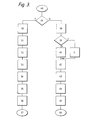
- pin T1 is first tested (step 49) to determine whether the interrupting device is the zero-crossing detector 10. If it is (branch "Y") the 8-bit counter CT and the register CTPLV are both set (steps 50 and 51) to the 256-complement of the eight least significant bits of the content of the firing angle register FAR which has previously been filled during the main program, as mentioned above. Moreover register TIBF is set in step 52 to the three most significant bits of the content of register FAR. In general triac 2 will be required to be fired a whole number N of cycles of counter CT plus a fraction of such a cycle after the zero-crossing instant, the contents of register FAR representing these quantities, as indicated above.
- step 50 counter CT will next overflow (generating a timer interrupt) after the said fraction of such a cycle, and because of step 52 the content of register TIBF indicates at which subsequent such overflow (or the same one) the triac should be fired.
- the content of register TIBF is first tested to see if it is zero, after which it is decremented. If the result of the test is zero the triac is actually fired, thus achieving the correct firing instant.
- the quantity stored in step 51 is used when the tachogenerator 11 produces an external interrupt, as will be described below.
- a record is kept in register TISLZC of the number of timer interrupts which have occurred since the last zero-crossing (again for use when the tachogenerator produces an external interrupt); this is the reason for step 53.
- a record is kept in register ZCSLTA of the number of zero-crossings which have occurred since the last tachogenerator interrupt (again for use when the tachogenerator produces an interrupt); this is the reason for step 54.
- the logic "0" pulse generated on pin P06 by means of steps 55 and 56 resets the bistable device 21.
- step 49 If it is determined in step 49 that the zero-crossing detector 10 is not the interrupting device, then the interrupting device must be the tachogenerator 11. In such a case branch "N" is carried out. More particularly, in step 58 the content of register NTT is transferred to register LTT. Then in step 59 it is tested whether the content of counter CT is less than a predetermined amount L. If it is not ("N") then in step 60 register NTT is filled with a quantity given by the concatenated contents of register TISLZC and counter CT less the content of register CTPLV.
- step 53 Because of step 53 and of the fact (as will be described with reference to Figure 4) that the content of register TISLZC is incremented each time a timer interrupt occurs, at any given time the contents of register TISLZC indicate how many timer interrupts have occurred since the last zero-crossing.
- the concatenated contents of register TISLZC and counter CT therefore represent the number of clock pulses generated by clock CL since the last zero-crossing occurred, i.e. the time period between the immediately preceding zero-crossing and the current tachogenerator output pulse. This quantity is therefore entered into register NTT.
- step 58 a corresponding quantity relating to the immediately preceding tachogenerator output pulse is already present in register LTT.
- the time (represented by a number of output pulses of clock CL) elapsing between these two tachogenerator output pulses (which is a measure of the current motor speed) is therefore given by the content of register NTT less the content of register LTT plus X times the number of output pulses of CL which corresponds to a complete half-cycle of the supply applied across terminals 3 and 4, where X is the number of zero-crossings which have occurred since the tachogenerator produced the preceding output pulse.
- register ZCSLTA Because of steps 54 and 63 the quantity X is contained in register ZCSLTA, this quantity being saved into register ZCSLTA * in step 62.
- the registers NTT, LTT and ZCSLTA' contain the quantities required by step 46 in the main program.
- the logic "0" pulse generated on output pin P07 by means of steps 64 and 65 resets the bistable device 24.
- the logic "0" pulse generated on pin P016 by means of steps 64 and 65 temporarily overrides the output signal of OR-function circuit 17, as described above, thereby producing a new transition from logic "1" to logic "0" at interrupt input 1 NT /TO if bistable device 21 should also be in the set state.
- step 60 is replaced by step 61, the difference being that the quantity 255 is used in the calculation instead of the content of counter CT.
- the relevant reading of counter CT will not follow the interrupt signal which gave rise to the relevant interrupt routine immediately, inter alia because the microcomputer 6 has first to store parameters to enable it to continue with its current program after the interrupt has been serviced, during which storage process the counter CT continues to count.
- the counter CT is thus read L counts after the interrupt signal occurs, where L may be of the order of ten, and thus the reading is too high by L. This does not normally matter, as it is the same for all readings.
- register TIBF is loaded in step 52 ( Figure 3) at each zero-crossing with the number of timer interrupts which should occur before the triac is actually fired, and is decremented (step 70) when each timer interrupt actually occurs, if when a given timer interrupt occurs the content of register TIBF is zero (test 68) then the triac should be fired immediately. This is accordingly done by means of step 69.
- a record is kept in register TISLZC of the number of timer interrupts which have occurred since the last zero-crossing (for use in steps 60 and 61 of Figure 3). This is the reason for the incrementing of the contents of this register in step 71 (and for their resetting to zero in step 53 of Figure 3).
- step 71 may be omitted provided that test 68 is now a test on the contents of register TISLZC for equality with the contents of register TIBF.
- steps 43, 45, 46 and 47 of the main program are only performed if a tachogenerator interrupt has been generated and processed by means of steps 58-66 since steps 43-47 were last performed. (Otherwise the main program would be duplicating a previous calculation).
- the branch of Figure 3 containing the steps 58-66 may include an operation (not shown) of setting a flag
- the main program of Figure 2 may include, after step 42, the steps (not shown) of testing and resetting this flag, the steps 43, 45, 46 and 47 only being performed if the flag is found to be set.
- step 58 of Figure 3 may be omitted if it is arranged that the results of the calculations carried out in step 60 (or 61) are written alternately into respective members of a pair of registers, a toggle being operated each time to indicate which register was last written and being tested in step 43 of Figure 2 to indicate which register corresponds to NTT and which to LTT.
- steps 43, 45 and 46 of the main program of Figure 2 can be carried out instead in the interrupt branch containing steps 58-66 of Figure 3, step 44 of Figure 2 then being transferred to after step 47.
- registers TIBF and TISLZC may be omitted, the various calculations and operations involving the contents of these re- giters being suitably modified or omitted accordingly.
Landscapes
- Engineering & Computer Science (AREA)
- Power Engineering (AREA)
- Control Of Ac Motors In General (AREA)
- Control Of Electric Motors In General (AREA)
Applications Claiming Priority (2)
| Application Number | Priority Date | Filing Date | Title |
|---|---|---|---|
| GB8610565 | 1986-04-30 | ||
| GB08610565A GB2189910A (en) | 1986-04-30 | 1986-04-30 | Motor speed control system |
Publications (3)
| Publication Number | Publication Date |
|---|---|
| EP0247650A2 true EP0247650A2 (de) | 1987-12-02 |
| EP0247650A3 EP0247650A3 (en) | 1989-07-26 |
| EP0247650B1 EP0247650B1 (de) | 1993-08-04 |
Family
ID=10597115
Family Applications (1)
| Application Number | Title | Priority Date | Filing Date |
|---|---|---|---|
| EP87200769A Expired - Lifetime EP0247650B1 (de) | 1986-04-30 | 1987-04-23 | Motorgeschwindigkeitsregelsystem |
Country Status (5)
| Country | Link |
|---|---|
| US (1) | US4771223A (de) |
| EP (1) | EP0247650B1 (de) |
| JP (1) | JPS62262685A (de) |
| DE (1) | DE3786837D1 (de) |
| GB (1) | GB2189910A (de) |
Cited By (4)
| Publication number | Priority date | Publication date | Assignee | Title |
|---|---|---|---|---|
| EP0428469A3 (en) * | 1989-11-14 | 1992-11-19 | Fagor. S.Coop. Ltda. | Digital speed controller for washing machine motors |
| FR2686168A1 (fr) * | 1992-01-14 | 1993-07-16 | Motorola Semiconducteurs | Circuit de commande de la vitesse d'un moteur. |
| GB2296608A (en) * | 1994-12-07 | 1996-07-03 | Mitsubishi Electric Corp | Motor drive unit for a fan |
| GB2301716A (en) * | 1995-06-01 | 1996-12-11 | Yang Tai Her | Phase angle control circuit for a switching device |
Families Citing this family (6)
| Publication number | Priority date | Publication date | Assignee | Title |
|---|---|---|---|---|
| JPH02159989A (ja) * | 1988-12-09 | 1990-06-20 | Sharp Corp | タイミング信号発生回路 |
| US5894095A (en) * | 1997-04-17 | 1999-04-13 | Demali; Gary W. | Mixing drill with speed sensing with multiple preset speeds |
| FR2767427B1 (fr) * | 1997-08-14 | 2000-04-28 | Moulinex Sa | Procede et systeme de variation et de regulation de vitesse d'un moteur |
| FR2767428B1 (fr) * | 1997-08-18 | 1999-11-19 | Moulinex Sa | Systeme et procede de regulation de vitesse pour moteur a excitation serie, et moteur correspondant |
| US7227326B1 (en) * | 2006-04-24 | 2007-06-05 | Rockwell Automation Technologies, Inc. | System and method for transient-based motor speed estimation with transient excitation |
| CN108336939B (zh) * | 2017-01-19 | 2023-03-24 | 尼得科电机有限公司 | 用于使用和控制永磁交流电动机的系统和方法 |
Family Cites Families (4)
| Publication number | Priority date | Publication date | Assignee | Title |
|---|---|---|---|---|
| US3110853A (en) * | 1958-06-05 | 1963-11-12 | Westinghouse Electric Corp | Electrical control apparatus |
| US4201936A (en) * | 1976-12-10 | 1980-05-06 | General Electric Company | Motor speed regulator and control system |
| AU2255583A (en) * | 1982-12-21 | 1984-06-28 | Sunbeam Corp. | Food preparation appliance |
| GB2147436A (en) * | 1983-09-28 | 1985-05-09 | Philips Electronic Associated | Variable motor speed control arrangement |
-
1986
- 1986-04-30 GB GB08610565A patent/GB2189910A/en not_active Withdrawn
-
1987
- 1987-04-21 US US07/040,910 patent/US4771223A/en not_active Expired - Fee Related
- 1987-04-23 EP EP87200769A patent/EP0247650B1/de not_active Expired - Lifetime
- 1987-04-23 DE DE8787200769T patent/DE3786837D1/de not_active Expired - Lifetime
- 1987-04-30 JP JP62107885A patent/JPS62262685A/ja active Pending
Cited By (6)
| Publication number | Priority date | Publication date | Assignee | Title |
|---|---|---|---|---|
| EP0428469A3 (en) * | 1989-11-14 | 1992-11-19 | Fagor. S.Coop. Ltda. | Digital speed controller for washing machine motors |
| FR2686168A1 (fr) * | 1992-01-14 | 1993-07-16 | Motorola Semiconducteurs | Circuit de commande de la vitesse d'un moteur. |
| EP0551627A1 (de) * | 1992-01-14 | 1993-07-21 | Motorola Semiconducteurs S.A. | Motorgeschwindigkeitsregelkreis |
| GB2296608A (en) * | 1994-12-07 | 1996-07-03 | Mitsubishi Electric Corp | Motor drive unit for a fan |
| GB2296608B (en) * | 1994-12-07 | 1999-03-24 | Mitsubishi Electric Corp | Motor unit, motor drive unit, fan unit and method of controlling the motor drive unit |
| GB2301716A (en) * | 1995-06-01 | 1996-12-11 | Yang Tai Her | Phase angle control circuit for a switching device |
Also Published As
| Publication number | Publication date |
|---|---|
| JPS62262685A (ja) | 1987-11-14 |
| GB2189910A (en) | 1987-11-04 |
| EP0247650A3 (en) | 1989-07-26 |
| US4771223A (en) | 1988-09-13 |
| GB8610565D0 (en) | 1986-06-04 |
| DE3786837D1 (de) | 1993-09-09 |
| EP0247650B1 (de) | 1993-08-04 |
Similar Documents
| Publication | Publication Date | Title |
|---|---|---|
| US4758945A (en) | Method for reducing power consumed by a static microprocessor | |
| US4748559A (en) | Apparatus for reducing power consumed by a static microprocessor | |
| US4771223A (en) | Motor speed control system | |
| JPH0795291B2 (ja) | ウオツチドツグタイマ | |
| JPS59146345A (ja) | コントロ−ルフロ−並列計算機方式 | |
| US4443848A (en) | Two-level priority circuit | |
| EP0082558B1 (de) | Steuersignalgeneratoranordnung für Halbleiterschalter | |
| JPH0450629B2 (de) | ||
| JPS5914396A (ja) | パルスモ−タ駆動装置 | |
| US4408328A (en) | Microprogram control circuit | |
| KR900002437B1 (ko) | 정보처리장치의 성능 조정 시스템 | |
| JPH02165721A (ja) | パルス出力装置 | |
| GB2189912A (en) | Data processing system; A.C. motor control | |
| GB2110441A (en) | Power supply control | |
| JP3098409B2 (ja) | 命令をリアル・タイムで処理する装置または方法 | |
| JPS63200234A (ja) | デ−タ処理装置 | |
| JPS5916054A (ja) | マイクロ・プロセツサ | |
| JP2557785Y2 (ja) | シングルチップマイクロコンピュータ | |
| JPH07118926B2 (ja) | モ−タのデイジタル制御装置 | |
| SU1677858A1 (ru) | Асинхронный распределитель | |
| JPS593563A (ja) | 計算機システム評価用タイマ | |
| JPH0767288B2 (ja) | サイリスタ・インバ−タのゲ−トパルス制御装置 | |
| CN116736786A (zh) | 一种实现plc控制设备计划任务队列的方法 | |
| JPH03246603A (ja) | 高速カウンタ | |
| JPH0695304B2 (ja) | デ−タ処理装置 |
Legal Events
| Date | Code | Title | Description |
|---|---|---|---|
| PUAI | Public reference made under article 153(3) epc to a published international application that has entered the european phase |
Free format text: ORIGINAL CODE: 0009012 |
|
| AK | Designated contracting states |
Kind code of ref document: A2 Designated state(s): DE ES FR GB IT |
|
| RAP3 | Party data changed (applicant data changed or rights of an application transferred) |
Owner name: PHILIPS ELECTRONIC AND ASSOCIATED INDUSTRIES LIMIT Owner name: N.V. PHILIPS' GLOEILAMPENFABRIEKEN |
|
| PUAL | Search report despatched |
Free format text: ORIGINAL CODE: 0009013 |
|
| AK | Designated contracting states |
Kind code of ref document: A3 Designated state(s): DE ES FR GB IT |
|
| 17P | Request for examination filed |
Effective date: 19900118 |
|
| 17Q | First examination report despatched |
Effective date: 19920211 |
|
| RAP3 | Party data changed (applicant data changed or rights of an application transferred) |
Owner name: PHILIPS ELECTRONICS UK LIMITED Owner name: N.V. PHILIPS' GLOEILAMPENFABRIEKEN |
|
| GRAA | (expected) grant |
Free format text: ORIGINAL CODE: 0009210 |
|
| AK | Designated contracting states |
Kind code of ref document: B1 Designated state(s): DE ES FR GB IT |
|
| PG25 | Lapsed in a contracting state [announced via postgrant information from national office to epo] |
Ref country code: IT Free format text: LAPSE BECAUSE OF FAILURE TO SUBMIT A TRANSLATION OF THE DESCRIPTION OR TO PAY THE FEE WITHIN THE PRE;WARNING: LAPSES OF ITALIAN PATENTS WITH EFFECTIVE DATE BEFORE 2007 MAY HAVE OCCURRED AT ANY TIME BEFORE 2007. THE CORRECT EFFECTIVE DATE MAY BE DIFFERENT FROM THE ONE RECORDED.SCRIBED TIME-LIMIT Effective date: 19930804 Ref country code: DE Effective date: 19930804 Ref country code: FR Effective date: 19930804 |
|
| REF | Corresponds to: |
Ref document number: 3786837 Country of ref document: DE Date of ref document: 19930909 |
|
| PG25 | Lapsed in a contracting state [announced via postgrant information from national office to epo] |
Ref country code: ES Free format text: LAPSE BECAUSE OF FAILURE TO SUBMIT A TRANSLATION OF THE DESCRIPTION OR TO PAY THE FEE WITHIN THE PRESCRIBED TIME-LIMIT Effective date: 19931115 |
|
| EN | Fr: translation not filed | ||
| PG25 | Lapsed in a contracting state [announced via postgrant information from national office to epo] |
Ref country code: GB Effective date: 19940423 |
|
| PLBE | No opposition filed within time limit |
Free format text: ORIGINAL CODE: 0009261 |
|
| STAA | Information on the status of an ep patent application or granted ep patent |
Free format text: STATUS: NO OPPOSITION FILED WITHIN TIME LIMIT |
|
| 26N | No opposition filed | ||
| GBPC | Gb: european patent ceased through non-payment of renewal fee |
Effective date: 19940423 |