EP0245765B1 - Datenübertragungssteuerungssystem - Google Patents
Datenübertragungssteuerungssystem Download PDFInfo
- Publication number
- EP0245765B1 EP0245765B1 EP87106567A EP87106567A EP0245765B1 EP 0245765 B1 EP0245765 B1 EP 0245765B1 EP 87106567 A EP87106567 A EP 87106567A EP 87106567 A EP87106567 A EP 87106567A EP 0245765 B1 EP0245765 B1 EP 0245765B1
- Authority
- EP
- European Patent Office
- Prior art keywords
- data
- phase
- basic clock
- clock
- node
- Prior art date
- Legal status (The legal status is an assumption and is not a legal conclusion. Google has not performed a legal analysis and makes no representation as to the accuracy of the status listed.)
- Expired - Lifetime
Links
Images


Classifications
-
- H—ELECTRICITY
- H04—ELECTRIC COMMUNICATION TECHNIQUE
- H04L—TRANSMISSION OF DIGITAL INFORMATION, e.g. TELEGRAPHIC COMMUNICATION
- H04L47/00—Traffic control in data switching networks
- H04L47/10—Flow control; Congestion control
- H04L47/28—Flow control; Congestion control in relation to timing considerations
-
- H—ELECTRICITY
- H04—ELECTRIC COMMUNICATION TECHNIQUE
- H04L—TRANSMISSION OF DIGITAL INFORMATION, e.g. TELEGRAPHIC COMMUNICATION
- H04L12/00—Data switching networks
- H04L12/28—Data switching networks characterised by path configuration, e.g. LAN [Local Area Networks] or WAN [Wide Area Networks]
- H04L12/42—Loop networks
- H04L12/422—Synchronisation for ring networks
-
- H—ELECTRICITY
- H04—ELECTRIC COMMUNICATION TECHNIQUE
- H04L—TRANSMISSION OF DIGITAL INFORMATION, e.g. TELEGRAPHIC COMMUNICATION
- H04L12/00—Data switching networks
- H04L12/28—Data switching networks characterised by path configuration, e.g. LAN [Local Area Networks] or WAN [Wide Area Networks]
- H04L12/42—Loop networks
- H04L12/427—Loop networks with decentralised control
- H04L12/433—Loop networks with decentralised control with asynchronous transmission, e.g. token ring, register insertion
-
- H—ELECTRICITY
- H04—ELECTRIC COMMUNICATION TECHNIQUE
- H04L—TRANSMISSION OF DIGITAL INFORMATION, e.g. TELEGRAPHIC COMMUNICATION
- H04L47/00—Traffic control in data switching networks
- H04L47/10—Flow control; Congestion control
-
- H—ELECTRICITY
- H04—ELECTRIC COMMUNICATION TECHNIQUE
- H04L—TRANSMISSION OF DIGITAL INFORMATION, e.g. TELEGRAPHIC COMMUNICATION
- H04L47/00—Traffic control in data switching networks
- H04L47/10—Flow control; Congestion control
- H04L47/13—Flow control; Congestion control in a LAN segment, e.g. ring or bus
-
- H—ELECTRICITY
- H04—ELECTRIC COMMUNICATION TECHNIQUE
- H04L—TRANSMISSION OF DIGITAL INFORMATION, e.g. TELEGRAPHIC COMMUNICATION
- H04L47/00—Traffic control in data switching networks
- H04L47/10—Flow control; Congestion control
- H04L47/30—Flow control; Congestion control in combination with information about buffer occupancy at either end or at transit nodes
Definitions
- This invention relates to a data transfer control system, which permits realization of circuit switching with a network of a token ring system as a local area networks system with the features of the first part of claim 1.
- EP-A-0 158 364 discloses a data transfer control system with the features of the first part of claim 1.
- a primary object of the invention is to eliminate the data buffer underflow due to token excursion time variation and realize circuit switching with a token ring system network.
- Another object of the invention is to provide, for the realization of circuit switching with the token ring system network, a synchronizing system, which permits establishment of synchronization between particular nodes in the network independently of the synchronization of the network as a whole and also of the communication speed in the network.
- a predetermined amount of data is stored in a data buffer under control of a controller, and also data transfer from the data buffer is started after the lapse of a predetermined period of time from the instant of setting-up of a data transfer mode.
- no underflow occurs in the receiving side data buffer.
- clock phase data is transmitted mutually as packets between nodes to establish the synchronization between the nodes.
- Fig. 1 is a block diagram showing an example of a node for carrying out the invention.
- a node 104 which comprises a ring transmission/reception control section 111 provided on a ring transmission line 103 for controlling transmission, reception, reproduction and repeating of transfer data, a transmission/reception data buffer 112 for temporarily storing transfer data, a terminal interface circuit 113 serving as an interface with respect to a terminal 101 and a controller 114 for collectively controlling the components 111 to 113.
- the terminal 101 is an exclusive transmission terminal, and it is connected through a terminal interface line 102 to the terminal interface circuit 113 of the node 104.
- the present invention concerns a data transfer control system in the controller 114 shown in Fig. 1, and an example of control sequence according to the invention will now be described with reference to the flow chart of Fig. 2.
- Fig. 2 shows an initial operation of the controller 114 until it is ready to start transmission of data from the terminal 101 to the ring transmission line 103 in response to a calling request from the terminal 101 or reception of a calling from a different node.
- a data transfer mode is set up after completion of a calling control mode (steps 121 and 122)
- transmission data from the terminal 101 starts to be fed to the transmission/reception data buffer 112 in the node 104, but the transmission of data to the ring transmission line 103 in a step 124 is enabled only after the lapse of a predetermined period of time in a step 123.
- the amount of data that is first sent out to the ring transmission line 103 is X ⁇ t w bits, and subsequently data stored in the transmission/reception data buffer 112 is sent out to the ring transmission line 103 every time of token arrival.
- the amount of data stored in the transmission/reception data buffer 112 is proportional to the elapsed time. Therefore, the judgement in the step 123 may be replaced with a check as to whether the predetermined data amount X ⁇ t w is reached by the data stored in the transmission/reception data buffer 112. Further, the storage capacity of the transmission/reception data buffer 112 should be over X ⁇ t w bits.
- FIG. 3 shows the manner of data transfer from node A to node B.
- Data flows from the terminal into the node A at a speed of X bits/sec.
- data flows out from the node B into the terminal at the same speed of X bits/sec.
- X ⁇ t w bits of data are transferred to be received in the node B.
- the node B starts to provide data to the terminal at the speed of X bits/sec. as soon as X ⁇ t w bits are received.
- the node A continues transmission to the ring transmission line while securing the token for every excursion.
- the amount of data that is remaining in the reception data buffer immediately before the node B receives new data in the n-th excursion form the ring transmission line in this situation is X ⁇ (t w - t B1 - t F2 + t F1 + t B1 + t B2 - t F3 ... - t Bn-2 - t Fu-1 + t Fu-2 + t Bn-2 - t Bn-1 - t Fu ) bits or, in a rearranged form, X ⁇ (t w + t F1 - t Fu-1 - t Bn-1 - t Fu ) bits. If this value is negative, there is an underflow in the data buffer.
- the underflow can be eliminated by satisfying a condition t w + t T ⁇ 1 - t Fu-1 - t Bn-1 - t Fu > 0 or t w > (t Fu-1 + t Bn-1 ) + (t Fu - T F1 ) .
- the maximum values of t Fu-1 + t Bn-1 and t Fu - t F1 are respectively t F (MAX) + t B (MAX) and t F (MAX) - t F (MIN).
- the former value corresponds to the maximum token excursion time, while the latter corresponds to the maximum inter-node forward delay time.
- the adjacent node is in the opposite direction to the direction, in which data is transmitted. Therefore, it will be seen that in the worst case double the maximum token excursion time suffices as the predetermined delay t w .
- the system according to the invention is realized with the transmitting side data buffer.
- the receiving side data buffer as shown in steps 131 to 134 of the flow chart of Fig. 4.
- the same effects as in the above embodiment may be obtained by arranging such that the predetermined delay t w is provided collectively by the transmitting and receiving side data buffers on the basis of the flow charts of Figs. 2 and 4.
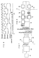
- Fig. 5 is a block diagram showing an essential part of the node according to the invention inclusive of a synchronizing circuit.
- the node 104 is connected by a transceiver 2 to a transmission line 103 constituting a network.
- Reference numeral 3 designates a transmission/reception controller having functions of medium access control in conformity to the network system and control of transmission and reception of data including basic clock phase data to be described later.
- Reference numeral 4 designates a transmitting side data buffer, in which is temporarily stored transmission data from the terminal 101 connected to the node through the terminal interface line 102.
- the data stored in the transmitting side data buffer 4 is sent out as bursts to the transmission line 103 when the node 104 secures a right of transmission with arrival of token or the like.
- Reference numeral 5 designates a receiving side data buffer, which receives and stores data addressed to the terminal 101 from the transmission line 103 and sends out the stored data continuously to the terminal 101.
- the speed of communication on the transmission line 103 is sufficiently high compared to the communication speed of the terminal 101, and a continuous data stream on the terminal interface line 102 corresponds to a data stream of data flowing burst-wise (or intermittently) in a time-compressed form through the transmission line 103.
- Reference numeral 6 designates a basic clock generator, and 7 a basic clock reproduction circuit, which is a featuring circuit as means for realizing the synchronizing system according to the invention.
- the function of the basic clock generator 6 is utilized when the node 104 is a clock master, while the function of the basic clock reproduction circuit 7 is utilized when the node is a clock slave.
- Reference numeral 8 designates a clock selector for supplying, to the terminal 101, either a master clock 14 of the basic clock generator 6 or a slave clock 15 of the basic clock reproduction circuit 7 according to a selector control 9 set by the operator or the like. It is conceivable to supply both the master and slave clocks 14 and 15 to the terminal 101 for the respective transmitting and receiving functions of the terminal 101.
- Reference numeral 113 designates a terminal interface circuit providing interface with respect to the transmitting and receiving side data buffers 4 and 5, clock selector 8 and terminal 101.
- a standard interface e.g., "RS232C" is provided to the terminal 101.
- Fig. 6 shows an example of the basic clock generator 6 in this embodiment.
- reference numeral 61 designates an oscillator, and 62 a frequency divider for providing intermediate value outputs.
- the frequency divider 62 is a one-eighth frequency divider. Its last stage output serves as a master clock 14 supplied to the terminal 101, and a 4-bit digital value of individual frequency division stages of ⁇ /8, ⁇ /4, ⁇ /2 and ⁇ is supplied as phase data of the master clock 14 to the transmission/reception controller 3.
- the frequency divider 62 permits a function of generating the master clock 14 and a function of generating the digital phase data of the master clock to be realized with a single circuit.
- Fig. 7 is a view showing a specific example of the basic clock generator 6 in the embodiment.
- reference numeral 61 designates an oscillator, 62 a frequency divider for providing intermediate value outputs, and 63 a master side master phase register for holding digital phase data of the frequency divider 62.
- the frequency divider 62 is a one-eighth frequency divider. Its last stage output serves as master clock 14 supplied to the terminal 101, and a 4-bit digital value of individual frequency division stages ⁇ /8, ⁇ /4, ⁇ /2 and ⁇ is supplied as digital phase data of the master clock 14 to the master side master phase register 63.
- the frequency divider 62 permits a function of generating the master clock 14 and a function of generating the digital phase data to be realized with a single circuit.
- Fig. 8 shows the input to and intermediate and last stage outputs of the frequency divider 62, i.e., a time chart of the master clock 14, indicating that the phase of one cycle (2 ⁇ ) of the master clock is digitalized in ⁇ /8 step, i.e., 4 bits.
- the master node transmits the newest digital phase data, i.e., digital phase data at the instant of start of transmission.
- Fig. 9 is a view showing an example of the basic clock reproduction circuit 7 in the embodiment.
- reference numeral 71 designates a 4-bit master phase register for holding the digital phase data which is transmitted from the master node and supplied through the transmission/reception controller 3, and 72 a slave phase register for holding the digital phase data of the slave clock 15.
- the contents of the registers 71 and 72 are updated according to a phase data reception pulse 31 which is provided from the transmission/reception controller 3 every time the master phase data is received.
- Reference numeral 73 designates a substracter which provides the phase difference between the contents of the registers 71 and 72.
- This phase difference is converted in a digital-to-analog (D/A) converter 74 into an analog voltage which is supplied to a voltage-controlled oscillator (VCO) 75 to control the oscillation frequency thereof.
- VCO voltage-controlled oscillator
- the output of the VCO 75 is supplied to a frequency divider 76 similar to the frequency divider shown in Fig. 7.
- the frequency divider 76 generates the slave clock 15 supplied to the terminal 101 as well as the digital phase data of the slave clock 15, these data being supplied to the slave phase register 72.
- the basic clock reproduction circuit 7 is basically the same as the prior art PLL except for that the phase data is sampled and compared, and the slave phase can be locked to the master phase on the basis of the sampling theorem so far as the variation of the phase difference is sufficiently small compared to the sampling period.
- Fig. 10 is a view showing a second example of the basic clock reproduction circuit 7.
- Reference numeral 76A in the Figure designates a variable frequency divider for frequency dividing a reproduction clock with a predetermined ratio to provide the slave clock 15 while also providing slave phase data, and 73A a subtracter as an operational circuit for performing subtraction of master phase data transmitted from the master node and supplied through the transmission/reception controller 3 and the slave phase data to obtain the difference between the master and slave phase data and supplying the error data thus obtained either entirely or partly as phase control data to the frequency divider 76A.
- a phase data reception pulse 31 is generated to be supplied to the variable frequency divider 76A to hold the value of the phase control data 71A at that moment.
- the variable frequency divider 76A adjusts the slave phase according to the held value to hold constant the error between the master and slave phases. More specifically, if the slave phase is lagging behind the master phase, the phase control data 71A has a positive value. In this case, the variable frequency divider 76A reduces the frequency division ratio to advance the slave phase. If the slave phase is leading the master phase, the phase control data 71A has a negative value. In this case, the variable frequency divider 76A increases the frequency division ratio to retard the slave phase. Fig.
- FIG. 11 shows a list of the error data, and in which 4-bit phase data are shown hexadecimally. It will be seen from Fig. 11 that the slave phase is the same as or lagging behind the master phase when the error data is 0 to 7 (i.e., positive) and is leading the master phase when the error data is 8 to F (i.e., negative). Therefore, it is possible to control the variable frequency divider 76A by utilizing only the sign bit (i.e., ⁇ phase data) of the error data. In the case of Fig. 10, the ⁇ phase of the error data is utilized as the phase control data 71A.
- Fig. 12 shows an example of the detailed construction of the variable frequency divider 76A. This circuit construction is well known.
- a J-K flip-flop FF3 merely frequency divides the reproduction clock 63 into one-half and constitutes a one-512-nd frequency divider with succeeding stage synchronous 4-bit counters C1 and C2.
- Fig. 13 is a time chart illustrating the operation of the variable frequency divider 76A when compensating for the delay of the slave phase.
- variable frequency divider shown in Fig. 12
- Fig. 13 the operation of the variable frequency divider shown in Fig. 12 will be explained with reference to Fig. 13.
- the phase control data 71A is "L"
- a flip-flop FF1a is set with the trailing end (fall) of the phase data reception pulse 31.
- the Q output of the flip-flop FF1a goes to "H” while the Q output of a flip-flop FF3 is “L”
- the AND condition is met, and the output of the AND gate G1a goes to "H”.
- the Q output of the flip-flop FF3 goes to "H” with the trailing end (fall) of the clock.
- the Q output of the flip-flop FF2a goes to "H"
- the flip-flop FF1a is reset.
- Fig. 14 is a time chart illustrating the operation of the variable frequency divider when the slave phase is leading the master phase. This operation is not described in detail.
- the slave phase is controlled to follow the master phase transmitted through a packet multiplex network.
- the number of frequency division stages of the variable frequency divider 76A and bit width of the master and slave phase data are suitably determined from the difference between the transmission and reception clocks, master phase transfer interval and allowable error between the master and slave phases.
- the synchronizing system permits present time data t n measured under control of the transmitting side clock (i.e., master clock) to be transmitted as phase data to the receiving side to correct the leading or lagging error ⁇ n of the receiving side clock (i.e., slave clock) t' n , wherein the slave clock is synchronized to the master clock.
- the transfer delay ⁇ has to be constant, but the transfer interval t n+1 - t n need not be constant, and the maximum transfer interval is determined by the extent of the error between the transmission and reception clocks.
- the transfer delay ⁇ as is obvious from a frame configuration as shown in Fig.
- data INFO is the phase data of the master clock.
- this data is a fixed length of 4 bits, so that the frame constitutes a packet having a fixed length.
- the transfer delay ⁇ is constant.
- a packet multiplex network e.g., a token ring or token bus network
- the upper limit of the transmission waiting time of each node is guaranteed by the excursion of the token or the like. Therefore, the above condition is met by making the constituent elements of the basic clock generator 6 and basic clock reproduction circuit 7 to be as precise as to be able to allow error between the transmission and reception clocks even when the transmission waiting time is maximum.
- the oscillation frequency of an oscillator 61 is frequency divided by a frequency divider 62 on the transmitting side, thus producing a master clock at a frequency of f0 Hz and phase data ⁇ 0 obtained through quantization in 1/8 ⁇ step.
- Phase data ⁇ 0 at the time t i of transmission is sampled and transmitted as data t i in a frame configuration as shown in Fig. 16 to the network.
- This phase data ⁇ 0 (t i ) reaches the receiving side after network transfer delay ⁇ and is subjected to serial-to-parallel conversion in a receiving register 3a in the transmission/reception controller 3.
- phase data reception pulse 31 based on the frame category FC of the received frame is generated from the transmission/reception controller 3.
- the phase data ⁇ 0 (t i ) is held in a master phase register 71, and phase data ⁇ c (t i + ⁇ ) of the f c -Hz slave clock at instant t i + ⁇ is sampled and held in a slave phase register 72.
- the phase data ⁇ 0 (t i ) and ⁇ c (t i + ⁇ ) held in the registers 71 and 72 are supplied to a subtracter 73 consisting of a complement circuit 73a and an adder 73b to obtain the phase difference between these two data.
- the phase difference is provided as digital data to a D/A converter 74 for conversion into analog data.
- the analog data is impressed as a control voltage proportional to the phase difference ⁇ 0 (t i )- ⁇ c (t i + ⁇ ) to a voltage-controlled oscillator 75.
- a voltage-controlled oscillator 75 In the voltage-controlled oscillator 75, its oscillation frequency is controlled according to the control voltage such that the phase difference is constant, and its output is supplied to a frequency divider 76.
- the frequency divider 76 frequency divides the oscillation frequency to generate a slave clock synchronized to the master clock and also phase data ⁇ c of the slave clock to be ready for the timing of reception of the next phase data reception pulse 31.
- the conditions required for the synchronization are that the network transfer delay ⁇ is constant and that the minimum sampling frequency 1/(t n+1 - t n ) max as specified by the transfer interval t u+1 - t n is at least double the maximum difference between the master and slave clock frequencies f0 and f c in accordance with the sampling theorem.
- the transfer delay ⁇ is constant as noted before, and by making the phase difference variation sufficiently small compared to the sampling cycle period by ensuring high accuracy of the individual clocks, the slave phase can be locked to the master phase, and it is possible to establish synchronization between particular nodes installed in a spaced-apart relation to one another via a network by permitting transmission of master phase data through the network.
- Fig. 18 shows a synchronizing system in case when the circuit shown in Fig. 5 is used as basic clock generation means.
- phase data ⁇ 0 transmitted in the frame configuration to the network reaches the receiving side after the network transfer delay ⁇ and is subjected to serial-to-parallel conversion in the receiving register 3a in the transmission/reception controller 3.
- a phase data reception pulse 31 based on the frame category FC of the reception frame is generated from the transmission/reception controller 3, and phase control data 71A obtained from a subtracter 73A is supplied at this timing to a variable frequency divider 76A for the variable frequency division control as noted above.
- the slave phase can be synchronized to the master phase.
- Circuit switching can be realized in a packet multiplex network if clock synchronization between nodes can be established.
- the oscillator 61 is provided in the basic clock generator 6. However, it is possible to process a clock supplied from the outside of the node like the output of the oscillator 61 for establishing synchronization between nodes under the control of the external clock.
- node 104 includes both the basic clock generator 6 and basic clock reproduction circuit 7. However, depending on the node it is possible to provide only either one of these two circuits.
- the synchronizing system as described it is possible to establish synchronization for circuit switching in a packet multiplex network, e.g., a token ring or token bus network, without need of dependency on the synchronization of the network as a whole and also on the communication speed in the network.
- a packet multiplex network e.g., a token ring or token bus network
Landscapes
- Engineering & Computer Science (AREA)
- Computer Networks & Wireless Communication (AREA)
- Signal Processing (AREA)
- Small-Scale Networks (AREA)
- Synchronisation In Digital Transmission Systems (AREA)
Claims (12)
- Datenübertragungssteuerungssystem zum Durchführen einer Datenübertragung eines Tokenringsystems, in welchem die Obergrenze der Übertragungswartezeit jedes Knotenpunktes (104) garantiert ist, wobei jeder Knotenpunkt (104) dem Passieren der Daten von/zu einem dazugehörigen, damit verbundenen Anschluß (101) zu/von besagtem Netzwerk dient und einen Datenpuffer (112) zum zeitweisen Speichern besagter Daten enthält, das Timing der Datenübertragung zu dem Netzwerk gesteuert ist, um eine konstante Verzögerung herzustellen, und von einem Grundtakterzeugungsmittel erzeugte Phasendaten eines Grundtaktgebers zu einem anderen Knotenpunkt (104) übertragen werden, gekennzeichnet durch eine Steuerung (114) zum Steuern einer Abrufsteuerung zwischen den Knotenpunkten (104) und der Datenübertragungssteuerung für besagten Datenpuffer (112) und das Grundtakterzeugungsmittel (6) zum Erzeugen einer Grundtaktrate für besagten Anschluß (101), wobei besagte Steuerung (114) dem Steuern des Timings der Datenübertragung zu besagtem Netzwerk dient, um eine konstante Verzögerungszeit zu liefern, und die von besagtem Grundtakterzeugungsmittel (6) erzeugten Phasendaten des Grundtaktgebers zu dem anderen Knotenpunkt (104) unter Benutzung eines Pakets übertragen werden, um Synchronisation des Grundtakts zur Datenübertragung zwischen besagtem anderen Knotenpunkt (104) und einem damit verbundenen Anschluß (101) zu erhalten.
- Datenübertragungssteuerungssystem nach Anspruch 1, dadurch gekennzeichnet, daß besagte konstante Verzögerungszeit doppelt so lang wie die maximale Tokenumlaufzeit durch den Tokenring ist.
- Datenübertragungssteuerungssystem nach Anspruch 1, dadurch gekennzeichnet, daß die Datenübertragung von einem übertragungsseitigen Datenpuffer (4) zu der Ringübertragungsleitung (103) nach einer vorherbestimmten Verzögerungszeit gestartet wird.
- Datenübertragungssteuerungssystem nach Anspruch 1, dadurch gekennzeichnet, daß die Datenübertragung von einem empfangsseitigen Datenpuffer (5) zu dem Anschluß (101) nach einer vorherbestimmten Verzögerungszeit gestartet wird.
- Datenübertragungssteuerungssystem nach Anspruch 1, dadurch gekennzeichnet, daß die Datenübertragung von dem übertragungsseitigen Datenpuffer (4) zu der Ringübertragungsleitung (103) und die Datenübertragung von dem empfangsseitigen Datenpuffer (5) zu dem Anschluß (101) nach Verzögerungszeiten gestartet werden, die zusammen eine vorherbestimmte Verzögerungszeit bilden.
- Datenübertragungssteuerungssystem nach Anspruch 1, dadurch gekennzeichnet, daß ein Knotenpunkt (104), der als ein Hauptsynchronisator beim Erreichen einer Taktsynchronisation zwischen den Knotenpunkten fungiert, das Grundtakterzeugungsmittel (8) zum Liefern eines Grundtakts an einen dazugehörigen Knotenpunkt und zum Erzeugen von Phasendaten von besagtem Grundtakt als Digitaldaten enthält, wobei besagte Digitalphasendaten aus vorherbestimmten Bits bestehen und als ein Paket dem Netzwerk zugesendet werden; daß ein Knotenpunkt, der als Nebensynchronisator fungiert, ein Grundtaktreproduktionsmittel (7) enthält, das mit besagten über das Netzwerk erhaltenen Digitalphasendaten auf das Steuerungsziel zuarbeitet, einen mit besagtem Grundtakt synchronisierten Takt zu reproduzieren; und daß Synchronisation zwischen bestimmten Knotenpunkten durch Lieferung der reproduzierten Taktrate an den angeschlossenen Anschluß (101) erreicht wird.
- Datenübertragungssteuerungssystem nach Anspruch 1, dadurch gekennzeichnet, daß jeder Knotenpunkt (104) sowohl ein Grundtakterzeugungsmittel (6) als auch ein Grundtaktreproduktionsmittel (7) enthält.
- Datenübertragungssteuerungssystem nach Anspruch 1, dadurch gekennzeichnet, daß jeder Knotenpunkt (104) entweder ein Grundtakterzeugungsmittel (6) oder ein Grundtaktreproduktionsmittel (7) enthält.
- Datenübertragungssteuerungssystem nach Anspruch 1, dadurch gekennzeichnet, daß besagtes Grundtakterzeugungsmittel (6) einen Oszillator (61) und einen Frequenzteiler (62) zum Frequenzteilen der Frequenz des Ausgangs besagten Oszillators (61) und auch zum Liefern digitaler Werte von individuellen Frequenzteilungsstadien enthält, um Phasendaten von besagtem Grundtakt zu bilden.
- Datenübertragungssteuerungssystem nach Anspurch 1, dadurch gekennzeichnet, daß besagtes Grundtakterzeugungsmittel (6) einen Frequenzteiler (62) zum Frequenzteilen einer extern gelieferten Taktrate enthält, um einen Grundtakt zu erzeugen, der an den Anschluß (101) weitergeben wird, während Digitalwerte von individuellen Frequenzteilungsstadien bereitgestellt werden, um Phasendaten von besagtem Grundtaktgeber zu bilden.
- Datenübertragungssteuerungssystem nach Anspurch 6, dadurch gekennzeichnet, daß besagtes Grundtaktreproduktionsmittel (7) ein Hauptphasenregister (71) zum Halten von über das Netzwerk empfangenen Digitalphasendaten, einen spannungsgesteuerten Oszillator (75) mit einer Oszillationsfrequenz, die in Übereinstimmung mit einer Steuerspannung steuerbar ist, einen Frequenzteiler (76) zum Frequenzteilen der Ausgangsfrequenz von besagtem Oszillator (75) zum Erzeugen eines an den Anschluß (101) weiterzugebenden Takts, während auch Digitalwerte von individuellen Frequenzteilungsstadien geliefert werden, um Phasendaten von besagtem Takt zu erzeugen, ein Nebenphasenregister (72) zum Halten der von besagtem Frequenzteiler (76) gelieferten Digitalphasendaten, einen Subtrahierer (73) zum Durchführen einer Subtraktion von besagtem Hauptphasenregister (71) und besagtem Nebenphasenregister (72), um den Phasenunterschied zu liefern, und einen Digital-Analog-Wandler (74) zum Wandeln des digitalen Ausgangs von besagtem Subtrahierer (73) in eine analoge, als eine Regelspannung dem besagten spannungsgesteurten Oszillator (75) zuzuführenden Spannung enthält.
- Datenübertragungssteuerungssystem nach Anspruch 1, dadurch gekennzeichnet, daß besagtes Grundtakterzeugungsmittel (6) einen variablen Frequenzteiler (76A), der Änderungen des Taktteilungsverhältnisses durchführen kann, und einen Operationsregelkreis (73A) zum Steuern des Frequenzteilungsverhältnisses von besagtem variablen Frequenzteiler (76A) durch Vergleich der über das Netzwerk empfangenen Hauptphase und der in besagtem variablen Frequenzteiler (76A) in dem Empfangsknotenpunkt erzeugten Nebenphase enthält, wodurch es besagter Nebenphase erlaubt ist, besagter Hauptphase zu folgen.
Applications Claiming Priority (8)
| Application Number | Priority Date | Filing Date | Title |
|---|---|---|---|
| JP11020186A JPS62266943A (ja) | 1986-05-14 | 1986-05-14 | デ−タ転送制御方式 |
| JP110201/86 | 1986-05-14 | ||
| JP151189/86 | 1986-06-27 | ||
| JP15118986 | 1986-06-27 | ||
| JP23194/87 | 1987-02-03 | ||
| JP62023193A JPH0783359B2 (ja) | 1986-06-27 | 1987-02-03 | 同期方式 |
| JP23193/87 | 1987-02-03 | ||
| JP62023194A JPH0783360B2 (ja) | 1986-06-27 | 1987-02-03 | 同期方式 |
Publications (3)
| Publication Number | Publication Date |
|---|---|
| EP0245765A2 EP0245765A2 (de) | 1987-11-19 |
| EP0245765A3 EP0245765A3 (en) | 1990-02-07 |
| EP0245765B1 true EP0245765B1 (de) | 1993-09-22 |
Family
ID=27457915
Family Applications (1)
| Application Number | Title | Priority Date | Filing Date |
|---|---|---|---|
| EP87106567A Expired - Lifetime EP0245765B1 (de) | 1986-05-14 | 1987-05-06 | Datenübertragungssteuerungssystem |
Country Status (5)
| Country | Link |
|---|---|
| US (1) | US4845709A (de) |
| EP (1) | EP0245765B1 (de) |
| AU (1) | AU580476B2 (de) |
| CA (1) | CA1282147C (de) |
| DE (1) | DE3787494T2 (de) |
Families Citing this family (38)
| Publication number | Priority date | Publication date | Assignee | Title |
|---|---|---|---|---|
| JPS6489737A (en) * | 1987-09-30 | 1989-04-04 | Toshiba Corp | Multiple address communication data transmission system |
| JP2749581B2 (ja) * | 1988-01-22 | 1998-05-13 | ユニバーサル販売 株式会社 | 遊技機用データ通信システム |
| GB2232857B (en) * | 1989-06-13 | 1993-09-01 | Research Machines Ltd | A flag counter circuit |
| JP2535615B2 (ja) * | 1989-08-14 | 1996-09-18 | 株式会社東芝 | デ―タ同期伝送方式 |
| JP2829091B2 (ja) * | 1990-04-19 | 1998-11-25 | 株式会社東芝 | データ処理システム |
| US5495474A (en) * | 1991-03-29 | 1996-02-27 | International Business Machines Corp. | Switch-based microchannel planar apparatus |
| US5742761A (en) * | 1991-03-29 | 1998-04-21 | International Business Machines Corporation | Apparatus for adapting message protocols for a switch network and a bus |
| US5206857A (en) * | 1991-04-29 | 1993-04-27 | At&T Bell Laboratories | Apparatus and method for timing distribution over an asynchronous ring |
| US5351242A (en) * | 1992-04-14 | 1994-09-27 | Marian Kramarczyk | Method and apparatus for configuring and maintaining token ring networks |
| US5539727A (en) * | 1992-04-14 | 1996-07-23 | Kramarczyk; Marian | Method and apparatus for configuring and maintaining token ring networks |
| US6263374B1 (en) | 1992-09-17 | 2001-07-17 | International Business Machines Corporation | Apparatus for coupling a bus-based architecture to a switch network |
| US6067408A (en) * | 1993-05-27 | 2000-05-23 | Advanced Micro Devices, Inc. | Full duplex buffer management and apparatus |
| US5598581A (en) * | 1993-08-06 | 1997-01-28 | Cisco Sytems, Inc. | Variable latency cut through bridge for forwarding packets in response to user's manual adjustment of variable latency threshold point while the bridge is operating |
| JP3441018B2 (ja) * | 1994-11-02 | 2003-08-25 | 富士通株式会社 | リング型伝送路の遅延制御方法および伝送装置 |
| JP3301682B2 (ja) * | 1995-08-11 | 2002-07-15 | 松下電器産業株式会社 | パケット出力装置 |
| US6028837A (en) * | 1996-08-27 | 2000-02-22 | National Semiconductor Corporation | Ether ring architecture for local area networks |
| US6027195A (en) * | 1996-11-12 | 2000-02-22 | Varis Corporation | System and method for synchronizing the piezoelectric clock sources of a plurality of ink jet printheads |
| JP3339786B2 (ja) * | 1996-12-02 | 2002-10-28 | オークマ株式会社 | 環状通信路におけるタイマー同期化装置および初期化方法 |
| US6091705A (en) * | 1996-12-20 | 2000-07-18 | Sebring Systems, Inc. | Method and apparatus for a fault tolerant, software transparent and high data integrity extension to a backplane bus or interconnect |
| US6581126B1 (en) | 1996-12-20 | 2003-06-17 | Plx Technology, Inc. | Method, system and apparatus for a computer subsystem interconnection using a chain of bus repeaters |
| US5896384A (en) | 1997-02-28 | 1999-04-20 | Intel Corporation | Method and apparatus for transferring deterministic latency packets in a ringlet |
| DE19803686A1 (de) * | 1998-01-30 | 1999-08-05 | Siemens Ag | Verfahren und Vorrichtung zur Kommunikation gleichberechtigter Stationen eines ringförmigen, seriellen Lichtwellenleiter-Busses |
| US6587857B1 (en) * | 1998-06-30 | 2003-07-01 | Citicorp Development Center, Inc. | System and method for warehousing and retrieving data |
| US7280549B2 (en) * | 2001-07-09 | 2007-10-09 | Micron Technology, Inc. | High speed ring/bus |
| US7123675B2 (en) * | 2002-09-25 | 2006-10-17 | Lucent Technologies Inc. | Clock, data and time recovery using bit-resolved timing registers |
| US7684413B2 (en) * | 2002-10-09 | 2010-03-23 | Juniper Networks, Inc. | System and method for rate agile adaptive clocking in a packet-based network |
| WO2006075321A2 (en) * | 2005-01-13 | 2006-07-20 | Vyyo Inc. | Device, system and method of communicating between circuit switch interfaces over an analog modulation communication network |
| US9286198B2 (en) | 2005-04-21 | 2016-03-15 | Violin Memory | Method and system for storage of data in non-volatile media |
| US8112655B2 (en) * | 2005-04-21 | 2012-02-07 | Violin Memory, Inc. | Mesosynchronous data bus apparatus and method of data transmission |
| US9582449B2 (en) | 2005-04-21 | 2017-02-28 | Violin Memory, Inc. | Interconnection system |
| US8452929B2 (en) | 2005-04-21 | 2013-05-28 | Violin Memory Inc. | Method and system for storage of data in non-volatile media |
| CN103116565A (zh) | 2005-04-21 | 2013-05-22 | 提琴存储器公司 | 可配置的开关原件、互连网络及布局网络间相互连接方法 |
| US9384818B2 (en) * | 2005-04-21 | 2016-07-05 | Violin Memory | Memory power management |
| US8028186B2 (en) | 2006-10-23 | 2011-09-27 | Violin Memory, Inc. | Skew management in an interconnection system |
| CN101836193B (zh) * | 2007-10-05 | 2012-10-03 | 提琴存储器公司 | 一种同步数据总线装置及数据传输方法 |
| US8823657B2 (en) * | 2010-09-07 | 2014-09-02 | Apple Inc. | Master/slave control of touch sensing |
| FI20195031A1 (fi) * | 2019-01-18 | 2020-07-19 | Exalocus Oy | Signaalien kulkuaikaeroon pohjautuva paikannus |
| US11818187B2 (en) * | 2019-08-31 | 2023-11-14 | Sonos, Inc. | Mixed-mode synchronous playback |
Family Cites Families (4)
| Publication number | Priority date | Publication date | Assignee | Title |
|---|---|---|---|---|
| US4716575A (en) * | 1982-03-25 | 1987-12-29 | Apollo Computer, Inc. | Adaptively synchronized ring network for data communication |
| US4525832A (en) * | 1982-07-07 | 1985-06-25 | Fuji Xerox Co., Ltd. | Digital signal transmission system |
| US4528661A (en) * | 1983-02-14 | 1985-07-09 | Prime Computer, Inc. | Ring communications system |
| US4663748A (en) * | 1984-04-12 | 1987-05-05 | Unisearch Limited | Local area network |
-
1987
- 1987-05-06 EP EP87106567A patent/EP0245765B1/de not_active Expired - Lifetime
- 1987-05-06 DE DE87106567T patent/DE3787494T2/de not_active Expired - Fee Related
- 1987-05-13 US US07/049,702 patent/US4845709A/en not_active Expired - Lifetime
- 1987-05-13 CA CA000536997A patent/CA1282147C/en not_active Expired - Lifetime
- 1987-05-14 AU AU72967/87A patent/AU580476B2/en not_active Ceased
Also Published As
| Publication number | Publication date |
|---|---|
| EP0245765A2 (de) | 1987-11-19 |
| DE3787494T2 (de) | 1994-04-28 |
| US4845709A (en) | 1989-07-04 |
| EP0245765A3 (en) | 1990-02-07 |
| DE3787494D1 (de) | 1993-10-28 |
| CA1282147C (en) | 1991-03-26 |
| AU7296787A (en) | 1987-11-19 |
| AU580476B2 (en) | 1989-01-12 |
Similar Documents
| Publication | Publication Date | Title |
|---|---|---|
| EP0245765B1 (de) | Datenübertragungssteuerungssystem | |
| US5353313A (en) | Transmission of a clock signal over an asynchronous data channel | |
| US4771426A (en) | Isochronous clock reconstruction | |
| US4592050A (en) | Apparatus and method for providing a transparent interface across a satellite communications link | |
| KR20000076918A (ko) | 무선 네트워크 | |
| JP2001513301A (ja) | Stm伝送システムによるatmにおける同期 | |
| AU556987B2 (en) | Synchronizing system | |
| US6011801A (en) | Rate control of channels on a time division multiplex bus | |
| RU2288543C2 (ru) | Способ и устройство для уменьшения фазовых скачков при переключении источников синхронизации | |
| JPH0783360B2 (ja) | 同期方式 | |
| JPH0783359B2 (ja) | 同期方式 | |
| US7783200B2 (en) | Method and apparatus for constant bit rate data transmission in an optical burst switching network | |
| US5333136A (en) | Parallel data transferring and processing circuit | |
| JP3538374B2 (ja) | 時刻供給システム及び時刻供給装置 | |
| NO135617B (de) | ||
| JPS60160236A (ja) | Pcm多重変換装置の同期方式 | |
| JP2010200277A (ja) | クロック同期方法及び通信システム | |
| JPH08335921A (ja) | Tfts通信同期回路 | |
| JP2730519B2 (ja) | スタッフ同期回路 | |
| JPH10336182A (ja) | Atm網内時刻同期方式 | |
| JP3315430B2 (ja) | パルス発生装置 | |
| JP2000224152A (ja) | 基準信号分配システム | |
| JPH03216028A (ja) | 衛星伝送システム | |
| JPH06164566A (ja) | 位相同期方式 | |
| JPS60235557A (ja) | ル−プ式伝送路間接続方式 |
Legal Events
| Date | Code | Title | Description |
|---|---|---|---|
| PUAI | Public reference made under article 153(3) epc to a published international application that has entered the european phase |
Free format text: ORIGINAL CODE: 0009012 |
|
| AK | Designated contracting states |
Kind code of ref document: A2 Designated state(s): DE FR GB |
|
| PUAL | Search report despatched |
Free format text: ORIGINAL CODE: 0009013 |
|
| AK | Designated contracting states |
Kind code of ref document: A3 Designated state(s): DE FR GB |
|
| 17P | Request for examination filed |
Effective date: 19900430 |
|
| 17Q | First examination report despatched |
Effective date: 19920331 |
|
| GRAA | (expected) grant |
Free format text: ORIGINAL CODE: 0009210 |
|
| AK | Designated contracting states |
Kind code of ref document: B1 Designated state(s): DE FR GB |
|
| REF | Corresponds to: |
Ref document number: 3787494 Country of ref document: DE Date of ref document: 19931028 |
|
| ET | Fr: translation filed | ||
| PLBE | No opposition filed within time limit |
Free format text: ORIGINAL CODE: 0009261 |
|
| STAA | Information on the status of an ep patent application or granted ep patent |
Free format text: STATUS: NO OPPOSITION FILED WITHIN TIME LIMIT |
|
| 26N | No opposition filed | ||
| REG | Reference to a national code |
Ref country code: GB Ref legal event code: 746 Effective date: 19960611 |
|
| REG | Reference to a national code |
Ref country code: FR Ref legal event code: D6 |
|
| PGFP | Annual fee paid to national office [announced via postgrant information from national office to epo] |
Ref country code: DE Payment date: 20010430 Year of fee payment: 15 |
|
| PGFP | Annual fee paid to national office [announced via postgrant information from national office to epo] |
Ref country code: GB Payment date: 20010502 Year of fee payment: 15 |
|
| PGFP | Annual fee paid to national office [announced via postgrant information from national office to epo] |
Ref country code: FR Payment date: 20010518 Year of fee payment: 15 |
|
| REG | Reference to a national code |
Ref country code: GB Ref legal event code: IF02 |
|
| PG25 | Lapsed in a contracting state [announced via postgrant information from national office to epo] |
Ref country code: GB Free format text: LAPSE BECAUSE OF NON-PAYMENT OF DUE FEES Effective date: 20020506 |
|
| PG25 | Lapsed in a contracting state [announced via postgrant information from national office to epo] |
Ref country code: DE Free format text: LAPSE BECAUSE OF NON-PAYMENT OF DUE FEES Effective date: 20021203 |
|
| GBPC | Gb: european patent ceased through non-payment of renewal fee |
Effective date: 20020506 |
|
| PG25 | Lapsed in a contracting state [announced via postgrant information from national office to epo] |
Ref country code: FR Free format text: LAPSE BECAUSE OF NON-PAYMENT OF DUE FEES Effective date: 20030131 |
|
| REG | Reference to a national code |
Ref country code: FR Ref legal event code: ST |