EP0242898B1 - Vorrichtung mit flachem Suszeptor, der parallel zu einer Referenzfläche um eine Achse lotrecht zu dieser Fläche rotiert - Google Patents
Vorrichtung mit flachem Suszeptor, der parallel zu einer Referenzfläche um eine Achse lotrecht zu dieser Fläche rotiert Download PDFInfo
- Publication number
- EP0242898B1 EP0242898B1 EP87200478A EP87200478A EP0242898B1 EP 0242898 B1 EP0242898 B1 EP 0242898B1 EP 87200478 A EP87200478 A EP 87200478A EP 87200478 A EP87200478 A EP 87200478A EP 0242898 B1 EP0242898 B1 EP 0242898B1
- Authority
- EP
- European Patent Office
- Prior art keywords
- disc
- rotation
- reference plane
- grooves
- groove
- Prior art date
- Legal status (The legal status is an assumption and is not a legal conclusion. Google has not performed a legal analysis and makes no representation as to the accuracy of the status listed.)
- Expired - Lifetime
Links
- 238000000034 method Methods 0.000 claims description 26
- 238000000927 vapour-phase epitaxy Methods 0.000 claims description 5
- 230000000295 complement effect Effects 0.000 claims description 4
- 238000000151 deposition Methods 0.000 claims description 4
- 230000008021 deposition Effects 0.000 claims description 4
- 238000004519 manufacturing process Methods 0.000 claims description 4
- 239000004065 semiconductor Substances 0.000 claims description 4
- 238000006073 displacement reaction Methods 0.000 claims description 3
- 238000005188 flotation Methods 0.000 claims 2
- 239000007789 gas Substances 0.000 description 66
- 239000000758 substrate Substances 0.000 description 19
- 238000000407 epitaxy Methods 0.000 description 9
- 230000004907 flux Effects 0.000 description 8
- 230000002349 favourable effect Effects 0.000 description 7
- 230000033001 locomotion Effects 0.000 description 7
- 239000000463 material Substances 0.000 description 6
- 238000012549 training Methods 0.000 description 6
- XYFCBTPGUUZFHI-UHFFFAOYSA-N Phosphine Chemical compound P XYFCBTPGUUZFHI-UHFFFAOYSA-N 0.000 description 4
- VYPSYNLAJGMNEJ-UHFFFAOYSA-N Silicium dioxide Chemical compound O=[Si]=O VYPSYNLAJGMNEJ-UHFFFAOYSA-N 0.000 description 4
- 239000012808 vapor phase Substances 0.000 description 4
- AZUYLZMQTIKGSC-UHFFFAOYSA-N 1-[6-[4-(5-chloro-6-methyl-1H-indazol-4-yl)-5-methyl-3-(1-methylindazol-5-yl)pyrazol-1-yl]-2-azaspiro[3.3]heptan-2-yl]prop-2-en-1-one Chemical compound ClC=1C(=C2C=NNC2=CC=1C)C=1C(=NN(C=1C)C1CC2(CN(C2)C(C=C)=O)C1)C=1C=C2C=NN(C2=CC=1)C AZUYLZMQTIKGSC-UHFFFAOYSA-N 0.000 description 3
- 238000010586 diagram Methods 0.000 description 3
- 238000010438 heat treatment Methods 0.000 description 3
- 239000001257 hydrogen Substances 0.000 description 3
- 229910052739 hydrogen Inorganic materials 0.000 description 3
- JBRZTFJDHDCESZ-UHFFFAOYSA-N AsGa Chemical compound [As]#[Ga] JBRZTFJDHDCESZ-UHFFFAOYSA-N 0.000 description 2
- IJGRMHOSHXDMSA-UHFFFAOYSA-N Atomic nitrogen Chemical compound N#N IJGRMHOSHXDMSA-UHFFFAOYSA-N 0.000 description 2
- 229910001218 Gallium arsenide Inorganic materials 0.000 description 2
- XUIMIQQOPSSXEZ-UHFFFAOYSA-N Silicon Chemical compound [Si] XUIMIQQOPSSXEZ-UHFFFAOYSA-N 0.000 description 2
- 238000000137 annealing Methods 0.000 description 2
- 239000012159 carrier gas Substances 0.000 description 2
- 150000001875 compounds Chemical class 0.000 description 2
- 230000007423 decrease Effects 0.000 description 2
- 239000000428 dust Substances 0.000 description 2
- 230000000694 effects Effects 0.000 description 2
- 230000005484 gravity Effects 0.000 description 2
- 150000002431 hydrogen Chemical class 0.000 description 2
- 238000005339 levitation Methods 0.000 description 2
- 229910000073 phosphorus hydride Inorganic materials 0.000 description 2
- 229920002120 photoresistant polymer Polymers 0.000 description 2
- 230000001902 propagating effect Effects 0.000 description 2
- 229910052710 silicon Inorganic materials 0.000 description 2
- 239000010703 silicon Substances 0.000 description 2
- 239000000377 silicon dioxide Substances 0.000 description 2
- OKTJSMMVPCPJKN-UHFFFAOYSA-N Carbon Chemical compound [C] OKTJSMMVPCPJKN-UHFFFAOYSA-N 0.000 description 1
- UFHFLCQGNIYNRP-UHFFFAOYSA-N Hydrogen Chemical compound [H][H] UFHFLCQGNIYNRP-UHFFFAOYSA-N 0.000 description 1
- 230000001133 acceleration Effects 0.000 description 1
- 230000009471 action Effects 0.000 description 1
- RBFQJDQYXXHULB-UHFFFAOYSA-N arsane Chemical compound [AsH3] RBFQJDQYXXHULB-UHFFFAOYSA-N 0.000 description 1
- 229910010293 ceramic material Inorganic materials 0.000 description 1
- 229910052681 coesite Inorganic materials 0.000 description 1
- 238000004320 controlled atmosphere Methods 0.000 description 1
- 238000007796 conventional method Methods 0.000 description 1
- 229910052906 cristobalite Inorganic materials 0.000 description 1
- 239000002178 crystalline material Substances 0.000 description 1
- 230000007547 defect Effects 0.000 description 1
- 238000011161 development Methods 0.000 description 1
- 238000009826 distribution Methods 0.000 description 1
- 239000012776 electronic material Substances 0.000 description 1
- 238000011156 evaluation Methods 0.000 description 1
- 230000005669 field effect Effects 0.000 description 1
- 229910002804 graphite Inorganic materials 0.000 description 1
- 239000010439 graphite Substances 0.000 description 1
- 230000004807 localization Effects 0.000 description 1
- 230000007246 mechanism Effects 0.000 description 1
- 229910052751 metal Inorganic materials 0.000 description 1
- 239000002184 metal Substances 0.000 description 1
- 150000002739 metals Chemical class 0.000 description 1
- 230000007935 neutral effect Effects 0.000 description 1
- 229910052757 nitrogen Inorganic materials 0.000 description 1
- 125000002524 organometallic group Chemical group 0.000 description 1
- 239000012071 phase Substances 0.000 description 1
- 238000000206 photolithography Methods 0.000 description 1
- 229920000642 polymer Polymers 0.000 description 1
- 230000008569 process Effects 0.000 description 1
- 238000012545 processing Methods 0.000 description 1
- 230000009467 reduction Effects 0.000 description 1
- 239000011819 refractory material Substances 0.000 description 1
- 229910052594 sapphire Inorganic materials 0.000 description 1
- 239000010980 sapphire Substances 0.000 description 1
- 235000012239 silicon dioxide Nutrition 0.000 description 1
- 230000000087 stabilizing effect Effects 0.000 description 1
- 229910052682 stishovite Inorganic materials 0.000 description 1
- 229910052905 tridymite Inorganic materials 0.000 description 1
Images






Classifications
-
- C—CHEMISTRY; METALLURGY
- C30—CRYSTAL GROWTH
- C30B—SINGLE-CRYSTAL GROWTH; UNIDIRECTIONAL SOLIDIFICATION OF EUTECTIC MATERIAL OR UNIDIRECTIONAL DEMIXING OF EUTECTOID MATERIAL; REFINING BY ZONE-MELTING OF MATERIAL; PRODUCTION OF A HOMOGENEOUS POLYCRYSTALLINE MATERIAL WITH DEFINED STRUCTURE; SINGLE CRYSTALS OR HOMOGENEOUS POLYCRYSTALLINE MATERIAL WITH DEFINED STRUCTURE; AFTER-TREATMENT OF SINGLE CRYSTALS OR A HOMOGENEOUS POLYCRYSTALLINE MATERIAL WITH DEFINED STRUCTURE; APPARATUS THEREFOR
- C30B25/00—Single-crystal growth by chemical reaction of reactive gases, e.g. chemical vapour-deposition growth
- C30B25/02—Epitaxial-layer growth
- C30B25/12—Substrate holders or susceptors
-
- C—CHEMISTRY; METALLURGY
- C23—COATING METALLIC MATERIAL; COATING MATERIAL WITH METALLIC MATERIAL; CHEMICAL SURFACE TREATMENT; DIFFUSION TREATMENT OF METALLIC MATERIAL; COATING BY VACUUM EVAPORATION, BY SPUTTERING, BY ION IMPLANTATION OR BY CHEMICAL VAPOUR DEPOSITION, IN GENERAL; INHIBITING CORROSION OF METALLIC MATERIAL OR INCRUSTATION IN GENERAL
- C23C—COATING METALLIC MATERIAL; COATING MATERIAL WITH METALLIC MATERIAL; SURFACE TREATMENT OF METALLIC MATERIAL BY DIFFUSION INTO THE SURFACE, BY CHEMICAL CONVERSION OR SUBSTITUTION; COATING BY VACUUM EVAPORATION, BY SPUTTERING, BY ION IMPLANTATION OR BY CHEMICAL VAPOUR DEPOSITION, IN GENERAL
- C23C16/00—Chemical coating by decomposition of gaseous compounds, without leaving reaction products of surface material in the coating, i.e. chemical vapour deposition [CVD] processes
- C23C16/44—Chemical coating by decomposition of gaseous compounds, without leaving reaction products of surface material in the coating, i.e. chemical vapour deposition [CVD] processes characterised by the method of coating
- C23C16/458—Chemical coating by decomposition of gaseous compounds, without leaving reaction products of surface material in the coating, i.e. chemical vapour deposition [CVD] processes characterised by the method of coating characterised by the method used for supporting substrates in the reaction chamber
- C23C16/4582—Rigid and flat substrates, e.g. plates or discs
- C23C16/4583—Rigid and flat substrates, e.g. plates or discs the substrate being supported substantially horizontally
- C23C16/4584—Rigid and flat substrates, e.g. plates or discs the substrate being supported substantially horizontally the substrate being rotated
Definitions
- the invention relates to a device comprising a plane disc rotating parallel to a reference plane and comprising a structure for centering this disc and structures arranged in the reference plane for bringing the disc into lift and rotation by the application of a gas flow at the rear face of this disc.
- the invention also relates to a vapor phase epitaxy reactor chamber provided with such a device.
- the invention finds its application in the production of rotating planar sample holders for an epitaxy chamber in the vapor phase, especially for the epitaxial growth in the vapor phase of layers of group III-V compounds to form semiconductor devices.
- the sample holder must be in good thermal contact with a heating device in order to prevent temperature variations in the sample, the latter causing variations in the homogeneity of the epitaxial layers produced on the surface. .
- the known device is intended for producing a layer of silica on a silicon substrate.
- a substrate is placed in a closed chamber and balanced on pins. It is also covered with a funnel-shaped mount with a flat bottom and large overturned opening.
- a gas flow is introduced through the funnel pipe and is distributed obliquely over the face of the facing substrate by a filter provided with several openings arranged at an angle to the plane of the substrate.
- the gases necessary for the deposition of SiO2 are brought in at the same time as the lift gas and the deposition takes place essentially on the face of the substrate which looks at the gas inlet orifices.
- the cited document teaches that under these conditions the substrate can also rotate.
- the known device consists of an annealing chamber for carrying out the step of annealing a layer of photoresist deposited on a semiconductor substrate in a photolithography process when carrying out an integrated circuit.
- a centering mount (jig) with a flat internal bottom for receiving the substrate and furthermore provided with flanges.
- the substrate does not rest directly on the flat bottom of the centering frame. he is arranged on shims, themselves placed on this flat bottom.
- the device further comprises means for lifting the substrate above the legs, so that it floats a small distance above the latter.
- levitation means consist of the arrival of a gas flow through a pipe which passes through the lower wall of the chamber. This pipe brings the gas flow to the underside of the flat bottom of said centering mount (jig) and is subdivided into four linear pipes, of smaller diameter, inclined on the vertical, so as to transport the flow by flaring toward the edges of the substrate.
- These small pipes pass through the wall of the flat bottom of the frame (jig) to lead to its upper surface exactly under the substrate mounted on wedges. Thus the flux can arrive at the lower surface of the substrate and put it in levitation above the shells.
- the known device also has means for rotating the substrate after it has been lifted.
- the four small linear pipes mentioned above are not only in an oblique position relative to the vertical axis embodied by the main flow supply pipe, but are also arranged tangentially to the latter. It is this arrangement which induces a rotational movement to the substrate when the flux is applied with a flow rate sufficient to cause a vortex movement by abutting on the edges of the frame.
- the known device also has means for heating the sample in the form of a microwave generator and a waveguide.
- the centering mount (jig) therefore constitutes the sample holder although it has contact with the sample only by means of shims.
- This sample holder, mount (jig) + wedges is not mobile. It is fixed. It is the sample alone which is lifted and rotated. All means of implementation lift and rotation are integral parts of the sample holder. In operation, the sample is no longer in contact with the sample holder.
- the microwave heater therefore heats the photoresist layer from the inside, but does not heat the substrate or the sample holder. In particular the whole room remains at low temperature.
- the gas flow which cooperates with the lift and the rotation of the substrate has no role in the operations of processing the sample.
- neither of these two cited implementations shows means for precise centering of the rotating sample.
- the means for floating and rotating the sample do not include any means specifically intended to produce the truly uniform rotation of this sample.
- the present invention provides a device with a rotating disc, applicable for example to a vapor phase epitaxy chamber as a sample holder, which makes it possible to solve these problems.
- the centering structure includes a first convex profile relative to one of the facing surfaces during the lift / rotation, it that is to say either on the surface of the reference plane, or on the lower surface of the disc, and includes a second concave profile complementary to the first, relative to the other facing surface respectively, the two profiles being nested one in the other so that the convex profile can rotate freely in the concave profile, while avoiding the lateral displacement of the disc, in that to put the disc in lift the reference plane comprises a first structure formed of n> 2 non-aligned orifices, made in the region delimited by the projection of the external edge of the disc, orifices through which a first gas flow is applied, perpendicular to the surface of the disc opposite the reference plane, so that a non-zero dimension h slot is obtained between the rear face of the disc and the reference plane, and in that for rotating the disc, the reference plane or the underside of
- the device according to the invention consists of a turntable 20, around an axis 30, parallel to a reference plane 10, the axis 30 being perpendicular to this plane.
- a disc-shaped tray preferably a disc-shaped tray will be chosen.
- this plate 20 is both maintained in lift above the surface 10, and rotated about the axis 30 by the action of a gas stream or several gas streams.
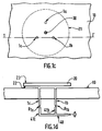
- FIG. 1a shows in section that the plate 20 is in lift at a distance h from the reference surface 10.
- the lift is obtained in the embodiment shown in FIG. 1a, by gas inlets 1a, 1b, ... 1n such that the system is in equilibrium, the gas inlet flow being on the other hand perpendicular to the plane plate 20 and plane 10.
- the gas injected by the inlets 1a, 1b, ... 1n, in the interval between the plate 20 and the reference surface 10 will find resistance to the flows in the slot 4 of height h , causing an increase in pressure on the surface 22 of the disc 20, relative to the ambient pressure.
- the gas flow will be expected to be large enough so that the difference between this pressure and the ambient pressure integrated on the surface 22 is at least equal to the force of gravity on the disc 20.
- the plate 20 must support a mass, for example a sample 100, which can be off-center.
- the system is asymmetrical and it must be ensured that the height h of the slot 4 remains at all points different from 0, that is to say that the distribution of the pressure on the lower surface 22 of the plate 20 also takes on a corresponding asymmetrical appearance, in which case the lift can be said to be stable.
- this preferential arrangement includes the arrival of gas by n > 2 non-aligned openings 1a, 1b, ... 1n.
- these orifices 1a ... 1n are deduced from each other by a rotation of 2 ⁇ / n.
- FIG. 1c represents seen from above the surface 10 of the reference wall.
- the trace of the lifted disc is represented at 21 by a broken line.
- Figure 1d shows the same system, in section along the axis II 'passing through the center of two of the openings 1b and 1c.
- This figure shows that these openings 1b and 1c are connected to a gas supply line 40, via the tubes 41b and 41c.
- the opening 1a which is not in the plane of Figure 1d, is likewise connected to the line 40 by a tube.
- the supplies 41a, 41b, 41c are provided with restrictions R 1a , R 1b , R 1c , constituting resistors R i .
- Each resistance R i is of value greater than or at least equivalent to the resistance R of the slot 4 in the part of this slot of height h situated between the arrival of the gas, for example 1a, located in the reference plane 10, and the ambient located around the system formed by the disc.
- FIG. 2 gives the equivalent diagram of the system provided with resistors R 1a , R 1b , R 1c .
- p A represents the supply pressure of one of the tubes, R i the resistance placed on this tube, R the resistance in the slot near the gas inlet and p S the lift pressure.
- the lift pressure isobars For a gas supply, for example 1a strongly offset from the axis of symmetry (or of rotation 30), the lift pressure isobars, represented in FIG. 3, show that, in the case where the height h of the slot 4 is the same at all points, the lift pressure applies predominantly near said opening 1a. Most of the flow, the local value of which is given by the distance between two isobars, passes through the region between the gas inlet orifice 1a and the edge 21 of the disc 20.
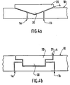
- FIGS. 4a and 4b each show a possible embodiment of this location by a profile cut out from the reference surface 10 and a profile complementary to the surface 22 of the disc 20. This type of location can be associated with several methods of rotating the disc exposed further.
- Rotational training can then be obtained by means of a method chosen from the two methods described below or by means of a composition of these two methods.
- the first method consists of a rotational drive by a force of viscosity.
- a force F V is applied to part of the surface 22 of the levitating disc.
- This force causes in the vicinity of this surface 22 a gas stream showing a speed component in the direction of rotation illustrated by the arrow T, as shown in Figures 5, which show two devices according to this method.
- F V is the force per unit area
- ⁇ V / ⁇ Z the derivative of its speed in the direction perpendicular to the surface 22.
- FIG. 5a An exemplary embodiment using the viscous force of a gas to obtain the rotation of the disc 20 described above, is shown in perspective in FIG. 5a, in exploded view in order to highlight the means of the rotation.
- the device according to the invention therefore comprises a disc 20 provided with an axis 30.
- the face 22 of the disc is, as has been said, essentially smooth.
- Rotational drive is obtained in the direction of arrow T owing to the fact that a gas flow ⁇ 2 is introduced into the groove 5 formed in the reference surface 10 by the inlet 2.
- This groove 5 is of rounded shape and of radius smaller than that of the disc , so that the flux ⁇ 2 can act on the latter by viscosity.
- the transverse dimension of the groove can be from 0.1 mm to several centimeters.
- the surface 10 further comprises, as has been said above, at least 3 orifices 1a, 1b, 1c for the arrival of the gas flow ⁇ 1 used for the lift.
- One or more gas flows can be used for the rotation of the disk 20.
- the supply of the arrivals 1a, 1b, 1c can be done according to a method illustrated by FIG. 1d.
- the supply to inlet 2 can also be done using this method.
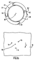
- FIG. 5b A second exemplary embodiment using the viscosity force of a gas to obtain the rotation of the disc 20 previously described, is shown in perspective in FIG. 5b, in exploded view, in order to highlight the means of the rotation.
- the device according to the invention therefore comprises a disc 20 provided with an axis 30.
- the face 22 of the disc 20 is here again essentially smooth.
- the rotary drive is obtained in the direction of the arrow T because a gas flow ⁇ 3 is introduced into the grooves 51a, 51b, 51c, formed in the reference surface 10, by the arrivals 1a, 1b respectively, 1 C.
- These grooves 51a, 51b, 51c are rounded in shape and do not extend beyond the trace 21 of the edge of the disc, so that the flow ⁇ 3 can act on the latter by viscosity.
- FIG. 5c represents an exemplary embodiment of these grooves seen from above.
- the number of grooves 51 may not be limited to three, just like the number of arrivals 1.
- the transverse dimension of the grooves can be from 0.1 mm to several centimeters and their depth from 10 ⁇ m to several millimeters
- each orifice 1a, 1b, 1c of gas inlet for the lift corresponds to a groove 51a, 51b , 51c for the rotation.
- these grooves are therefore advantageously made in the reference plane 10, rather than in the surface 22.
- the second method of rotational training mentioned above consists of training by inertial forces.
- the gas transmits then to the disc part of its momentum, this momentum is proportional to ⁇ .v2, ⁇ being the mass of the gas per unit of volume, which is written: F i ⁇ ⁇ .V2 4 / or what can also be written: F i ⁇ ⁇ . Deb2 5 /
- FIGS. 6a and 6b An exemplary embodiment, using the inertial forces of a gas to obtain the rotation of the disc 20 previously described, is shown in FIGS. 6a and 6b.
- FIG. 6a shows the arrangement of grooves 61, 62, 63, 64 formed in the surface 22 of the disc 20 and which constitute the structures against which the gas flow but abuts.
- these structures will preferably be produced at the periphery of the disc 20, as has been said previously.
- grooves 61, 62, 63, 64 are fed by a circular groove 7, which can be made either in the reference plane 10, as shown in FIG. 6a, or in the surface 22 of the disc as shown in FIG. 6b, where it then opens directly onto said grooves 61, 62, 63, 64.
- one or more gas flows are sufficient to lift and rotate a disc.
- the viscosity ⁇ is not, in the first order, a function of the pressure, and this for all gases, provided that this pressure is sufficiently high so that the free path of the molecules does not exceed the characteristic dimension of the structure traversed, here the thickness of the slot 4 which is h (typically 50 ⁇ m to 100 ⁇ m).
- This method of drive and lift is applicable to all gases at all pressures beyond this limit, that is to say in practice above 0.1 mbar.
- This invention can be advantageously applied to the production of sample holders for a vapor phase epitaxy chamber.
- the sample holder 20 is brought to a temperature of the order of 600 ° C to 850 ° C, by proximity to the reference plane 10 constituted by the lower wall of the epitaxy chamber which transmits heat from a source.
- the deposition in the gas phase is done using materials in gaseous form mixed for example with hydrogen which then constitutes a carrier gas.
- the disc 20 is lifted and rotated respectively by a flow gas arriving through the openings 1a, 1b, 1c not aligned and propagating in the rounded grooves 51a, 51b, 51c.
- a flow gas arriving through the openings 1a, 1b, 1c not aligned and propagating in the rounded grooves 51a, 51b, 51c.
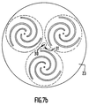
- the disc 201 is thus associated with the orifices 201a, 201b, 201c.
- the disks 202 and 203 are themselves associated each with three orifices not shown in FIG. 7a for reasons of simplicity of the drawing.
- Each of the orifices corresponds to a curved groove, for example as shown in FIG. 7b which is a representation of the surface 23 of the disc 20.
- the corresponding grooves are denoted 251a, 251b, and 251c.
- the samples are placed on the surfaces 223 of the disks 201, 202, 203.
- the principle of rotation is that which is illustrated by FIG. 5b, and described previously.
- the different discs according to the invention can be made of all hard materials with low deformation, including polymers.
- these materials must also be refractory. It can be: graphite, metals, ceramic materials, crystalline materials such as silicon, gallium arsenide, sapphire.
- the suitable gases can be chosen from hydrogen, nitrogen and all neutral gases. However, other gases can be chosen for specific applications not mentioned.
- a device according to the invention is particularly advantageous for obtaining the rotation stop in a determined position. This is particularly useful for loading and unloading samples in the case of planetary rotation.
- FIG. 8 This device represents the orifices and the grooves made in the reference surface 10, on the one hand, and the grooves made in the surface 22 of the sample-carrying disk on the other hand.
- the reference surface 10 comprises the axis of rotation 30, and three grooves 51a, 51b and 51c produced near the trace 21 of the edge of the disc. This surface further comprises, opening into these three grooves, three radial grooves 52a, 52b and 52c respectively.
- the grooves 52a, 52b and 52c are supplied by the three orifices 1a, 1b, 1c respectively as already described above.
- the surface 22 of the disc 20 has a circular groove 53 concentric with the axis of rotation and located near the latter, which is called the central groove.
- the surface 22 further comprises three radial grooves 71a, 71b, 71c.
- the central groove 53 can be produced in the reference surface 10.
- an orifice 54 connected to a pipe closed by a valve.
- This orifice 54, said central orifice, is made opposite, or opening into the central groove 53.
Landscapes
- Chemical & Material Sciences (AREA)
- General Chemical & Material Sciences (AREA)
- Chemical Kinetics & Catalysis (AREA)
- Engineering & Computer Science (AREA)
- Materials Engineering (AREA)
- Metallurgy (AREA)
- Organic Chemistry (AREA)
- Crystallography & Structural Chemistry (AREA)
- Mechanical Engineering (AREA)
- Crystals, And After-Treatments Of Crystals (AREA)
- Chemical Vapour Deposition (AREA)
Claims (13)
- Vorrichtung mit einer flachen Platte (20), die parallel zu einer Bezugsebene (10) drehbar ist und eine Struktur zum Zentrieren dieser Platte und Strukturen in der Bezugsebene enthält, um durch Zufuhr einer Gasströmung an der Rückseite der Platte diese Platte in den Schwebezustand und in den Rotationszustand zu bringen, dadurch gekennzeichnet, daß die Zentrierstruktur ein erstes, in bezug auf eine der einander gegenüberliegenden Flächen beim Schweben/Rotieren konvexes Profil (30), d.h. in bezug auf die Fläche der Bezugsebene (10) oder auf die untere Fläche der Platte (22), und ein zweites konkaves, dem ersten Profil komplementäres Profil in bezug auf die andere jeweils gegenüberliegende Fläche enthält, wobei die zwei Profile derart ineinander verschachtelt sind, daß das konvexe Profil sich im konkaven Profil ohne seitliche Verlagerung der Platte frei drehen kann, daß zum Erhalten des Schwebezustands der Platte die Bezugsebene eine erste, aus n) 2 nicht ausgerichteten Öffnungen (1a, 1b, 1c) gebildete Struktur in einem von der Projektion des Außenrandes der Platte begrenzten Bereichs enthält, wobei durch die Öffnungen senkrecht zur Plattenoberfläche in bezug auf die Bezugsebene ein erster gasförmiger Fluß (φ1) zugeführt wird, so daß zwischen der Rückfläche der Platte und der Bezugsebene ein Spalt mit der Nicht-Null-Abmessung h entsteht, und daß zum Erhalten der Rotation der Platte die Bezugsebene oder die untere Fläche der Platte eine zweite Struktur (5, 51a-51b-51c, 7) enthält, die durch wenigstens eine gerundete Rille gebildet wird, in der ein zweiter gasförmiger Fluß (φ2, φ3, φ4) umläuft und die sich in dem für die Rotation gewählten Sinn dreht.
- Vorrichtung nach Anspruch 1, dadurch gekennzeichnet, daß das erste konvexe Profil (30) ein Zylinder mit geringem Durchmesser gegenüber dem Durchmesser der Platte (20) ist, der auf der Fläche der Bezugsebene (10) angeordnet ist, und das zweite konkave Profil ein zylindrischer Hohlraum mit komplementären Abmessungen an der unteren Fläche (22) und in der Mitte der Platte (20) ist, und daß die Öffnungen der ersten Struktur sich durch eine Rotation von 2π/η ableitbar sind.
- Vorrichtung nach Anspruch 2, dadurch gekennzeichnet, daß zum Erhalten des Rotationszustands der schwebenden Platte nach einem genannten Verfahren durch eine Viskositätskraft einerseits die zweite Struktur (5) sich in der Bezugsebene befindet und außerdem eine Öffnung (2) enthält, die zum Zuführen eines zweiten Gasflusses (φ2) in die gerundete Rille mündet und sie speist, wobei diese Rille in dem von der Projektion des Außenrandes der Platte begrenzten Bereich verwirklicht wird, diesem Plattenrand folgt und sich in der für die Rotation gewählten Richtung dreht, und andererseits diese Rille außerhalb des vom Außenrand der Platte begrenzten Bereichs endet.
- Vorrichtung nach Anspruch 2, dadurch gekennzeichnet, daß zum Erhalten des Rotationszustands der schwebenden Platte nach einem genannten Verfahren durch eine Viskositätskraft die zweite Struktur sich in der Bezugsebene befindet und n gerundete Rillen (51a, 51b, 51c) enthält, in die jeweils die n Öffnungen (1a, 1b, 1c) münden, durch die der bzw. die erste(n) Fluß bzw. Flüsse (φ1, φ3) zum Erhalten des Schwebezustands zugeführt wird bzw. werden, wobei diese Rillen von den Öffnungen in einer für die Rotation vorgesehenen Richtung drehen und dabei in dem durch die Projektion des Außenrandes des Auflagers begrenzten Bereich bleiben.
- Vorrichtung nach Anspruch 2, dadurch gekennzeichnet, daß zum Erhalten des Rotationszustands der schwebenden Platte nach einem genannten Verfahren durch eine Trägheitskraft die Rille der zweiten Struktur (7) sich in der Bezugsebene befindet und kreisförmig ist, ihr Durchmesser kleiner als der Durchmesser der Platte ist, und daß die Platte weiter eine sog. dritte Struktur (61, 62, 63, 64) enthält, die durch n' U-förmige Rillen gebildet wird, die durch eine Rotation von 2π/η abgeleitbar sind, einerseits auf den Pegel der kreisförmigen Rille (7) der Bezugsebene und zum anderen an den Rand der Platte münden.
- Vorrichtung nach Anspruch 2, dadurch gekennzeichnet, daß zum Erhalten des Rotationszustands der schwebenden Platte nach einem genannten Verfahren durch eine Trägheitskraft die Rille der zweiten Struktur (7) sich in der unteren Fläche der Platte befindet und einerseits durch eine kreisförmige Rille mit einem Durchmesser Kleiner als der Durchmesser der dazu konzentrischen Platte und zum anderen durch n' U-förmige Rillen (61, 62, 63, 64) gebildet wird, die durch eine Rotation von 2π/n' ableitbar sind, einerseits in die kreisförmige Rille und andererseits an den Rand der Platte münden.
- Vorrichtung nach einem der Ansprüche 5 oder 6, dadurch gekennzeichnet, daß n' = 4 ist.
- Vorrichtung nach Anspruch 2, dadurch gekennzeichnet, daß zum Erhalten des Rotationszustands der schwebenden Platte nach einem genannten Verfahren durch eine Viskositätskraft die zweite Struktur sich in der Bezugsebene befindet und folgende Elemente umfaßt:a) n gekrümmte Rillen (51a, 51b, 51c) parallel zum Plattenrand.b) n radial angeordnete Rillen (52a, 52b, 52c) in dem durch die Projektion des Randes der Platte begrenzten Bereich mit einer Abmessung kleiner als die des Plattenstrahls, wobei in diese Rillen jeweils die n Öffnungen (1a, 1b, 1c) münden, durch die der Fluß (die Flüsse) zum Erhalten des Schwebezustands zugeführt wird und in die die n gekrümmten Rillen münden,c) eine zur Rotationsachse konzentrische und in der Nähe dieser Achse liegende sog. zentrale Rille (53),d) eine sog. zentrale Öffnung in Verbindung mit einem durch einen Schieber abgeschlossenen Ausgang, der in die zentrale Rille mündet, daß die untere Fläche der Platte weiter eine sog. dritte Struktur enthält, die durch n radiale Rillen (71a, 71b, 71c) mit einer Abmessung Kleiner als die des Strahls der n parallel zur Plattenrand verlaufenden Rillen (51a, 51b, 51c) der Bezugsebene gebildet wird (auf der Fläche gegenüber der Bezugsebene verwirklicht), wobei diese n radialen Rillen auf den Pegel der zentralen Rille (53) münden, und daß zum Stoppen der Platte in den n möglichen Positionen, in denen die radialen Rillen der Platte mit den radialen Rillen der Bezugsebene zusammenfallen, der (die) nach den n Öffnungen (1a, 1b, 1c) der Bezugsebene zugeführte(n) Fluß (Flüsse) gleichzeitig mit dem Öffnen des Schiebers für die zentrale Öffnung abgeschlossen wird (werden).
- Vorrichtung nach einem der Ansprüche 3 bis 8, dadurch gekennzeichnet, daß die Platte auf ihrer Fläche (23) gegenüber der Bezugsebene n" sog. sekundäre Platten (201, 202, 203) enthält, deren Position durch eine Rotation von 2π/n" ableitbar ist, wobei die Platte mit einer der n" sekundären Platten selbst eine Vorrichtung nach einem der Ansprüche 3 bis 8 bildet.
- Vorrichtung nach Anspruch 9, dadurch gekennzeichnet, daß n" = 3 ist.
- Vorrichtung nach einem der Ansprüche 1 bis 10, dadurch gekennzeichnet, daß n = 3 ist.
- Reaktionskammer für Epitaxie in der Dampfphase, dadurch gekennzeichnet, daß sie zur Bildung eines Probenträgers wenigstens eine Vorrichtung nach einem oder mehreren der Ansprüche 1 bis 11 enthält.
- Verfahren zur Verwirklichung einer Halbleitervorrichtung, dadurch gekennzeichnet, daß es die Ablagerung von Epitaxialschichten mittels der Kammer nach Anspruch 12 umfaßt.
Applications Claiming Priority (2)
| Application Number | Priority Date | Filing Date | Title |
|---|---|---|---|
| FR8604078 | 1986-03-21 | ||
| FR8604078A FR2596070A1 (fr) | 1986-03-21 | 1986-03-21 | Dispositif comprenant un suscepteur plan tournant parallelement a un plan de reference autour d'un axe perpendiculaire a ce plan |
Publications (2)
| Publication Number | Publication Date |
|---|---|
| EP0242898A1 EP0242898A1 (de) | 1987-10-28 |
| EP0242898B1 true EP0242898B1 (de) | 1993-07-28 |
Family
ID=9333382
Family Applications (1)
| Application Number | Title | Priority Date | Filing Date |
|---|---|---|---|
| EP87200478A Expired - Lifetime EP0242898B1 (de) | 1986-03-21 | 1987-03-16 | Vorrichtung mit flachem Suszeptor, der parallel zu einer Referenzfläche um eine Achse lotrecht zu dieser Fläche rotiert |
Country Status (5)
| Country | Link |
|---|---|
| US (1) | US4860687A (de) |
| EP (1) | EP0242898B1 (de) |
| JP (1) | JPH0778276B2 (de) |
| DE (1) | DE3786692T2 (de) |
| FR (1) | FR2596070A1 (de) |
Cited By (1)
| Publication number | Priority date | Publication date | Assignee | Title |
|---|---|---|---|---|
| DE102017105947A1 (de) | 2017-03-20 | 2018-09-20 | Aixtron Se | Suszeptor für einen CVD-Reaktor |
Families Citing this family (171)
| Publication number | Priority date | Publication date | Assignee | Title |
|---|---|---|---|---|
| FR2628984B1 (fr) * | 1988-03-22 | 1990-12-28 | Labo Electronique Physique | Reacteur d'epitaxie a planetaire |
| FR2628985B1 (fr) * | 1988-03-22 | 1990-12-28 | Labo Electronique Physique | Reacteur d'epitaxie a paroi protegee contre les depots |
| FR2638020B1 (fr) * | 1988-10-14 | 1990-12-28 | Labo Electronique Physique | Reacteur d'epitaxie a collecteur de gaz ameliore |
| US5155062A (en) * | 1990-12-20 | 1992-10-13 | Cree Research, Inc. | Method for silicon carbide chemical vapor deposition using levitated wafer system |
| US5226383A (en) * | 1992-03-12 | 1993-07-13 | Bell Communications Research, Inc. | Gas foil rotating substrate holder |
| JPH06310438A (ja) * | 1993-04-22 | 1994-11-04 | Mitsubishi Electric Corp | 化合物半導体気相成長用基板ホルダおよび化合物半導体気相成長装置 |
| US5558721A (en) * | 1993-11-15 | 1996-09-24 | The Furukawa Electric Co., Ltd. | Vapor phase growth system and a gas-drive motor |
| US5888304A (en) * | 1996-04-02 | 1999-03-30 | Applied Materials, Inc. | Heater with shadow ring and purge above wafer surface |
| US5468299A (en) * | 1995-01-09 | 1995-11-21 | Tsai; Charles S. | Device comprising a flat susceptor rotating parallel to a reference surface about a shaft perpendicular to this surface |
| US5702532A (en) * | 1995-05-31 | 1997-12-30 | Hughes Aircraft Company | MOCVD reactor system for indium antimonide epitaxial material |
| DE19628620A1 (de) * | 1995-08-08 | 1998-01-29 | Heidelberger Druckmasch Ag | Leiteinrichtung für einen frisch bedruckten Bogen |
| US6053982A (en) | 1995-09-01 | 2000-04-25 | Asm America, Inc. | Wafer support system |
| US6113702A (en) * | 1995-09-01 | 2000-09-05 | Asm America, Inc. | Wafer support system |
| US6183565B1 (en) * | 1997-07-08 | 2001-02-06 | Asm International N.V | Method and apparatus for supporting a semiconductor wafer during processing |
| US5747113A (en) * | 1996-07-29 | 1998-05-05 | Tsai; Charles Su-Chang | Method of chemical vapor deposition for producing layer variation by planetary susceptor rotation |
| US5788777A (en) * | 1997-03-06 | 1998-08-04 | Burk, Jr.; Albert A. | Susceptor for an epitaxial growth factor |
| JP2000511705A (ja) * | 1997-04-10 | 2000-09-05 | ユニフェイズ オプト ホールディングス インコーポレイテッド | 半導体デバイスの製造方法及びこの方法を実施する装置 |
| US6005226A (en) * | 1997-11-24 | 1999-12-21 | Steag-Rtp Systems | Rapid thermal processing (RTP) system with gas driven rotating substrate |
| US6449428B2 (en) * | 1998-12-11 | 2002-09-10 | Mattson Technology Corp. | Gas driven rotating susceptor for rapid thermal processing (RTP) system |
| JP2000192234A (ja) * | 1998-12-28 | 2000-07-11 | Matsushita Electric Ind Co Ltd | プラズマ処理装置 |
| NL1011017C2 (nl) | 1999-01-13 | 2000-07-31 | Asm Int | Inrichting voor het positioneren van een wafer. |
| NL1011487C2 (nl) * | 1999-03-08 | 2000-09-18 | Koninkl Philips Electronics Nv | Werkwijze en inrichting voor het roteren van een wafer. |
| US7083327B1 (en) * | 1999-04-06 | 2006-08-01 | Thermal Wave Imaging, Inc. | Method and apparatus for detecting kissing unbond defects |
| NL1012004C2 (nl) | 1999-05-07 | 2000-11-13 | Asm Int | Werkwijze voor het verplaatsen van wafers alsmede ring. |
| US6464795B1 (en) | 1999-05-21 | 2002-10-15 | Applied Materials, Inc. | Substrate support member for a processing chamber |
| NL1013989C2 (nl) * | 1999-12-29 | 2001-07-02 | Asm Int | Werkwijze en inrichting voor het behandelen van een wafer. |
| NL1013984C2 (nl) | 1999-12-29 | 2001-07-02 | Asm Int | Werkwijze en inrichting voor het behandelen van substraten. |
| EP1273031B1 (de) * | 2000-04-13 | 2005-08-10 | NanoPhotonics AG | Modulares messsystem für substrate |
| US7494927B2 (en) | 2000-05-15 | 2009-02-24 | Asm International N.V. | Method of growing electrical conductors |
| US6679951B2 (en) | 2000-05-15 | 2004-01-20 | Asm Intenational N.V. | Metal anneal with oxidation prevention |
| DE10056029A1 (de) * | 2000-11-11 | 2002-05-16 | Aixtron Ag | Verfahren und Vorrichtung zur Temperatursteuerung der Oberflächentemperaturen von Substraten in einem CVD-Reaktor |
| JP4537566B2 (ja) | 2000-12-07 | 2010-09-01 | 大陽日酸株式会社 | 基板回転機構を備えた成膜装置 |
| US7797966B2 (en) * | 2000-12-29 | 2010-09-21 | Single Crystal Technologies, Inc. | Hot substrate deposition of fused silica |
| US6569250B2 (en) | 2001-01-08 | 2003-05-27 | Cree, Inc. | Gas-driven rotation apparatus and method for forming silicon carbide layers |
| US6709721B2 (en) | 2001-03-28 | 2004-03-23 | Applied Materials Inc. | Purge heater design and process development for the improvement of low k film properties |
| NL1018086C2 (nl) * | 2001-05-16 | 2002-11-26 | Asm Int | Werkwijze en inrichting voor het thermisch behandelen van substraten. |
| WO2002097867A1 (de) * | 2001-05-29 | 2002-12-05 | Aixtron Ag | Aus einem tragkörper und darauf gasgelagerten und drehangetriebenen substrathalter bestehende anordnung |
| DE10133914A1 (de) * | 2001-07-12 | 2003-01-23 | Aixtron Ag | Prozesskammer mit abschnittsweise unterschiedlich drehangetriebenem Boden und Schichtabscheideverfahren in einer derartigen Prozesskammer |
| US6896738B2 (en) * | 2001-10-30 | 2005-05-24 | Cree, Inc. | Induction heating devices and methods for controllably heating an article |
| US7104578B2 (en) * | 2002-03-15 | 2006-09-12 | Asm International N.V. | Two level end effector |
| US6797069B2 (en) * | 2002-04-08 | 2004-09-28 | Cree, Inc. | Gas driven planetary rotation apparatus and methods for forming silicon carbide layers |
| US6843201B2 (en) * | 2002-05-08 | 2005-01-18 | Asm International Nv | Temperature control for single substrate semiconductor processing reactor |
| US7427329B2 (en) * | 2002-05-08 | 2008-09-23 | Asm International N.V. | Temperature control for single substrate semiconductor processing reactor |
| US6788991B2 (en) | 2002-10-09 | 2004-09-07 | Asm International N.V. | Devices and methods for detecting orientation and shape of an object |
| EP1570108B1 (de) * | 2002-12-10 | 2009-02-18 | E.T.C. Epitaxial Technology Center SRL | Suszeptorsystem |
| CN100507073C (zh) * | 2002-12-10 | 2009-07-01 | Etc外延技术中心有限公司 | 感受器系统 |
| US7181132B2 (en) | 2003-08-20 | 2007-02-20 | Asm International N.V. | Method and system for loading substrate supports into a substrate holder |
| US7410355B2 (en) * | 2003-10-31 | 2008-08-12 | Asm International N.V. | Method for the heat treatment of substrates |
| US7022627B2 (en) | 2003-10-31 | 2006-04-04 | Asm International N.V. | Method for the heat treatment of substrates |
| US6883250B1 (en) | 2003-11-04 | 2005-04-26 | Asm America, Inc. | Non-contact cool-down station for wafers |
| US6940047B2 (en) * | 2003-11-14 | 2005-09-06 | Asm International N.V. | Heat treatment apparatus with temperature control system |
| ATE501286T1 (de) * | 2004-06-09 | 2011-03-15 | E T C Epitaxial Technology Ct Srl | Halterungssystem für behandlungsapparaturen |
| US20060045667A1 (en) * | 2004-07-14 | 2006-03-02 | Savas Stephen E | Substrate handling system and process for manufacturing large substrates |
| US7217670B2 (en) * | 2004-11-22 | 2007-05-15 | Asm International N.V. | Dummy substrate for thermal reactor |
| US7666773B2 (en) | 2005-03-15 | 2010-02-23 | Asm International N.V. | Selective deposition of noble metal thin films |
| US8025922B2 (en) | 2005-03-15 | 2011-09-27 | Asm International N.V. | Enhanced deposition of noble metals |
| DE102005024118B4 (de) * | 2005-05-25 | 2009-05-07 | Mattson Thermal Products Gmbh | Vorrichtung und Verfahren zur Reduktion von Partikeln bei der thermischen Behandlung rotierender Substrate |
| JP2009502039A (ja) * | 2005-07-21 | 2009-01-22 | エルピーイー ソシエタ ペル アチオニ | ウェーハ処理装置の処理室の中でサセプタを支持し回転させるためのシステム |
| US8052794B2 (en) * | 2005-09-12 | 2011-11-08 | The United States Of America As Represented By The Secretary Of The Navy | Directed reagents to improve material uniformity |
| US8628622B2 (en) * | 2005-09-12 | 2014-01-14 | Cree, Inc. | Gas driven rotation apparatus and method for forming crystalline layers |
| DE102006018514A1 (de) * | 2006-04-21 | 2007-10-25 | Aixtron Ag | Vorrichtung und Verfahren zur Steuerung der Oberflächentemperatur eines Substrates in einer Prozesskammer |
| US8004740B2 (en) * | 2006-11-09 | 2011-08-23 | International Business Machines Corporation | Device and system for reflective digital light processing (DLP) |
| DE102006056289A1 (de) * | 2006-11-29 | 2008-06-05 | Bankmann, Joachim, Dr. | Beschichtungsanlage mit einer Funkvorrichtung sowie Verfahren zur Steuerung eines Aktors bzw. einer Heizung |
| US20080171436A1 (en) * | 2007-01-11 | 2008-07-17 | Asm Genitech Korea Ltd. | Methods of depositing a ruthenium film |
| DE102007026348A1 (de) | 2007-06-06 | 2008-12-11 | Aixtron Ag | Verfahren und Vorrichtung zur Temperatursteuerung der Oberflächentemperaturen von Substraten in einem CVD-Reaktor |
| KR101544198B1 (ko) | 2007-10-17 | 2015-08-12 | 한국에이에스엠지니텍 주식회사 | 루테늄 막 형성 방법 |
| US7655564B2 (en) | 2007-12-12 | 2010-02-02 | Asm Japan, K.K. | Method for forming Ta-Ru liner layer for Cu wiring |
| US8092606B2 (en) * | 2007-12-18 | 2012-01-10 | Asm Genitech Korea Ltd. | Deposition apparatus |
| US7799674B2 (en) | 2008-02-19 | 2010-09-21 | Asm Japan K.K. | Ruthenium alloy film for copper interconnects |
| US8847249B2 (en) | 2008-06-16 | 2014-09-30 | Soraa, Inc. | Solid-state optical device having enhanced indium content in active regions |
| US8805134B1 (en) | 2012-02-17 | 2014-08-12 | Soraa Laser Diode, Inc. | Methods and apparatus for photonic integration in non-polar and semi-polar oriented wave-guided optical devices |
| US8143148B1 (en) | 2008-07-14 | 2012-03-27 | Soraa, Inc. | Self-aligned multi-dielectric-layer lift off process for laser diode stripes |
| US8259769B1 (en) | 2008-07-14 | 2012-09-04 | Soraa, Inc. | Integrated total internal reflectors for high-gain laser diodes with high quality cleaved facets on nonpolar/semipolar GaN substrates |
| US8124996B2 (en) | 2008-08-04 | 2012-02-28 | Soraa, Inc. | White light devices using non-polar or semipolar gallium containing materials and phosphors |
| US8284810B1 (en) | 2008-08-04 | 2012-10-09 | Soraa, Inc. | Solid state laser device using a selected crystal orientation in non-polar or semi-polar GaN containing materials and methods |
| US8084104B2 (en) | 2008-08-29 | 2011-12-27 | Asm Japan K.K. | Atomic composition controlled ruthenium alloy film formed by plasma-enhanced atomic layer deposition |
| US8133555B2 (en) | 2008-10-14 | 2012-03-13 | Asm Japan K.K. | Method for forming metal film by ALD using beta-diketone metal complex |
| US9379011B2 (en) | 2008-12-19 | 2016-06-28 | Asm International N.V. | Methods for depositing nickel films and for making nickel silicide and nickel germanide |
| US8634442B1 (en) | 2009-04-13 | 2014-01-21 | Soraa Laser Diode, Inc. | Optical device structure using GaN substrates for laser applications |
| DE112010001615T5 (de) | 2009-04-13 | 2012-08-02 | Soraa, Inc. | Stuktur eines optischen Elements unter Verwendung von GaN-Substraten für Laseranwendungen |
| US8242522B1 (en) | 2009-05-12 | 2012-08-14 | Soraa, Inc. | Optical device structure using non-polar GaN substrates and growth structures for laser applications in 481 nm |
| US8254425B1 (en) | 2009-04-17 | 2012-08-28 | Soraa, Inc. | Optical device structure using GaN substrates and growth structures for laser applications |
| US8294179B1 (en) | 2009-04-17 | 2012-10-23 | Soraa, Inc. | Optical device structure using GaN substrates and growth structures for laser applications |
| US8837545B2 (en) | 2009-04-13 | 2014-09-16 | Soraa Laser Diode, Inc. | Optical device structure using GaN substrates and growth structures for laser applications |
| US8416825B1 (en) | 2009-04-17 | 2013-04-09 | Soraa, Inc. | Optical device structure using GaN substrates and growth structure for laser applications |
| US10108079B2 (en) | 2009-05-29 | 2018-10-23 | Soraa Laser Diode, Inc. | Laser light source for a vehicle |
| US9829780B2 (en) | 2009-05-29 | 2017-11-28 | Soraa Laser Diode, Inc. | Laser light source for a vehicle |
| US8427590B2 (en) | 2009-05-29 | 2013-04-23 | Soraa, Inc. | Laser based display method and system |
| US9800017B1 (en) | 2009-05-29 | 2017-10-24 | Soraa Laser Diode, Inc. | Laser device and method for a vehicle |
| US9250044B1 (en) | 2009-05-29 | 2016-02-02 | Soraa Laser Diode, Inc. | Gallium and nitrogen containing laser diode dazzling devices and methods of use |
| US8247887B1 (en) | 2009-05-29 | 2012-08-21 | Soraa, Inc. | Method and surface morphology of non-polar gallium nitride containing substrates |
| US8509275B1 (en) | 2009-05-29 | 2013-08-13 | Soraa, Inc. | Gallium nitride based laser dazzling device and method |
| US8329569B2 (en) | 2009-07-31 | 2012-12-11 | Asm America, Inc. | Deposition of ruthenium or ruthenium dioxide |
| US8314429B1 (en) | 2009-09-14 | 2012-11-20 | Soraa, Inc. | Multi color active regions for white light emitting diode |
| US8355418B2 (en) | 2009-09-17 | 2013-01-15 | Soraa, Inc. | Growth structures and method for forming laser diodes on {20-21} or off cut gallium and nitrogen containing substrates |
| US8750342B1 (en) | 2011-09-09 | 2014-06-10 | Soraa Laser Diode, Inc. | Laser diodes with scribe structures |
| US8933644B2 (en) | 2009-09-18 | 2015-01-13 | Soraa, Inc. | LED lamps with improved quality of light |
| US9293644B2 (en) | 2009-09-18 | 2016-03-22 | Soraa, Inc. | Power light emitting diode and method with uniform current density operation |
| US9583678B2 (en) | 2009-09-18 | 2017-02-28 | Soraa, Inc. | High-performance LED fabrication |
| CN107256915A (zh) | 2009-09-18 | 2017-10-17 | 天空公司 | 发光二极管器件 |
| DE102009044276A1 (de) * | 2009-10-16 | 2011-05-05 | Aixtron Ag | CVD-Reaktor mit auf einem mehrere Zonen aufweisenden Gaspolster liegenden Substrathalter |
| US8905588B2 (en) | 2010-02-03 | 2014-12-09 | Sorra, Inc. | System and method for providing color light sources in proximity to predetermined wavelength conversion structures |
| US10147850B1 (en) | 2010-02-03 | 2018-12-04 | Soraa, Inc. | System and method for providing color light sources in proximity to predetermined wavelength conversion structures |
| US9927611B2 (en) | 2010-03-29 | 2018-03-27 | Soraa Laser Diode, Inc. | Wearable laser based display method and system |
| US20110247556A1 (en) * | 2010-03-31 | 2011-10-13 | Soraa, Inc. | Tapered Horizontal Growth Chamber |
| US8451876B1 (en) | 2010-05-17 | 2013-05-28 | Soraa, Inc. | Method and system for providing bidirectional light sources with broad spectrum |
| JP4676567B1 (ja) * | 2010-07-20 | 2011-04-27 | 三井造船株式会社 | 半導体基板熱処理装置 |
| KR20120014361A (ko) * | 2010-08-09 | 2012-02-17 | 삼성엘이디 주식회사 | 서셉터 및 이를 포함하는 화학증착장치 |
| US8816319B1 (en) | 2010-11-05 | 2014-08-26 | Soraa Laser Diode, Inc. | Method of strain engineering and related optical device using a gallium and nitrogen containing active region |
| US9048170B2 (en) | 2010-11-09 | 2015-06-02 | Soraa Laser Diode, Inc. | Method of fabricating optical devices using laser treatment |
| US8975615B2 (en) | 2010-11-09 | 2015-03-10 | Soraa Laser Diode, Inc. | Method of fabricating optical devices using laser treatment of contact regions of gallium and nitrogen containing material |
| US9318875B1 (en) | 2011-01-24 | 2016-04-19 | Soraa Laser Diode, Inc. | Color converting element for laser diode |
| US9025635B2 (en) | 2011-01-24 | 2015-05-05 | Soraa Laser Diode, Inc. | Laser package having multiple emitters configured on a support member |
| US9595813B2 (en) | 2011-01-24 | 2017-03-14 | Soraa Laser Diode, Inc. | Laser package having multiple emitters configured on a substrate member |
| US9093820B1 (en) | 2011-01-25 | 2015-07-28 | Soraa Laser Diode, Inc. | Method and structure for laser devices using optical blocking regions |
| US9236530B2 (en) | 2011-04-01 | 2016-01-12 | Soraa, Inc. | Miscut bulk substrates |
| US9287684B2 (en) | 2011-04-04 | 2016-03-15 | Soraa Laser Diode, Inc. | Laser package having multiple emitters with color wheel |
| US8871617B2 (en) | 2011-04-22 | 2014-10-28 | Asm Ip Holding B.V. | Deposition and reduction of mixed metal oxide thin films |
| US9646827B1 (en) | 2011-08-23 | 2017-05-09 | Soraa, Inc. | Method for smoothing surface of a substrate containing gallium and nitrogen |
| US8971370B1 (en) | 2011-10-13 | 2015-03-03 | Soraa Laser Diode, Inc. | Laser devices using a semipolar plane |
| DE102012101923B4 (de) | 2012-03-07 | 2019-11-07 | Osram Opto Semiconductors Gmbh | Substratträgeranordnung, Beschichtungsanlage mit Substratträgeranordnung und Verfahren zur Durchführung eines Beschichtungsverfahrens |
| US9020003B1 (en) | 2012-03-14 | 2015-04-28 | Soraa Laser Diode, Inc. | Group III-nitride laser diode grown on a semi-polar orientation of gallium and nitrogen containing substrates |
| US10559939B1 (en) | 2012-04-05 | 2020-02-11 | Soraa Laser Diode, Inc. | Facet on a gallium and nitrogen containing laser diode |
| US9800016B1 (en) | 2012-04-05 | 2017-10-24 | Soraa Laser Diode, Inc. | Facet on a gallium and nitrogen containing laser diode |
| US9343871B1 (en) | 2012-04-05 | 2016-05-17 | Soraa Laser Diode, Inc. | Facet on a gallium and nitrogen containing laser diode |
| US9088135B1 (en) | 2012-06-29 | 2015-07-21 | Soraa Laser Diode, Inc. | Narrow sized laser diode |
| US9184563B1 (en) | 2012-08-30 | 2015-11-10 | Soraa Laser Diode, Inc. | Laser diodes with an etched facet and surface treatment |
| TW201437421A (zh) * | 2013-02-20 | 2014-10-01 | Applied Materials Inc | 用於旋轉料架原子層沉積之裝置以及方法 |
| KR20150125923A (ko) * | 2013-02-27 | 2015-11-10 | 토요 탄소 가부시키가이샤 | 서셉터 |
| US9166372B1 (en) | 2013-06-28 | 2015-10-20 | Soraa Laser Diode, Inc. | Gallium nitride containing laser device configured on a patterned substrate |
| US10022745B2 (en) * | 2013-08-01 | 2018-07-17 | Veeco Precision Surface Processing Llc | Apparatus for dual speed spin chuck |
| JP6058515B2 (ja) * | 2013-10-04 | 2017-01-11 | 漢民科技股▲分▼有限公司 | 気相成膜装置 |
| US9362715B2 (en) | 2014-02-10 | 2016-06-07 | Soraa Laser Diode, Inc | Method for manufacturing gallium and nitrogen bearing laser devices with improved usage of substrate material |
| US9368939B2 (en) | 2013-10-18 | 2016-06-14 | Soraa Laser Diode, Inc. | Manufacturable laser diode formed on C-plane gallium and nitrogen material |
| US9520695B2 (en) | 2013-10-18 | 2016-12-13 | Soraa Laser Diode, Inc. | Gallium and nitrogen containing laser device having confinement region |
| US9379525B2 (en) | 2014-02-10 | 2016-06-28 | Soraa Laser Diode, Inc. | Manufacturable laser diode |
| CN103614779B (zh) * | 2013-11-28 | 2016-03-16 | 中国电子科技集团公司第五十五研究所 | 一种提高碳化硅外延片片内n型掺杂浓度均匀性的方法 |
| US9209596B1 (en) | 2014-02-07 | 2015-12-08 | Soraa Laser Diode, Inc. | Manufacturing a laser diode device from a plurality of gallium and nitrogen containing substrates |
| US9871350B2 (en) | 2014-02-10 | 2018-01-16 | Soraa Laser Diode, Inc. | Manufacturable RGB laser diode source |
| US9520697B2 (en) | 2014-02-10 | 2016-12-13 | Soraa Laser Diode, Inc. | Manufacturable multi-emitter laser diode |
| US9564736B1 (en) * | 2014-06-26 | 2017-02-07 | Soraa Laser Diode, Inc. | Epitaxial growth of p-type cladding regions using nitrogen gas for a gallium and nitrogen containing laser diode |
| US20160033070A1 (en) * | 2014-08-01 | 2016-02-04 | Applied Materials, Inc. | Recursive pumping member |
| US12126143B2 (en) | 2014-11-06 | 2024-10-22 | Kyocera Sld Laser, Inc. | Method of manufacture for an ultraviolet emitting optoelectronic device |
| US9246311B1 (en) | 2014-11-06 | 2016-01-26 | Soraa Laser Diode, Inc. | Method of manufacture for an ultraviolet laser diode |
| US9653642B1 (en) | 2014-12-23 | 2017-05-16 | Soraa Laser Diode, Inc. | Manufacturable RGB display based on thin film gallium and nitrogen containing light emitting diodes |
| US9666677B1 (en) | 2014-12-23 | 2017-05-30 | Soraa Laser Diode, Inc. | Manufacturable thin film gallium and nitrogen containing devices |
| CN104810248B (zh) * | 2015-04-08 | 2017-08-08 | 中国电子科技集团公司第五十五研究所 | 适用于4°和8°偏轴硅面碳化硅衬底的原位处理方法 |
| US11437775B2 (en) | 2015-08-19 | 2022-09-06 | Kyocera Sld Laser, Inc. | Integrated light source using a laser diode |
| US11437774B2 (en) | 2015-08-19 | 2022-09-06 | Kyocera Sld Laser, Inc. | High-luminous flux laser-based white light source |
| US10879673B2 (en) | 2015-08-19 | 2020-12-29 | Soraa Laser Diode, Inc. | Integrated white light source using a laser diode and a phosphor in a surface mount device package |
| US10938182B2 (en) | 2015-08-19 | 2021-03-02 | Soraa Laser Diode, Inc. | Specialized integrated light source using a laser diode |
| JP2017055086A (ja) * | 2015-09-11 | 2017-03-16 | 昭和電工株式会社 | SiCエピタキシャルウェハの製造方法及びSiCエピタキシャルウェハの製造装置 |
| US9607842B1 (en) | 2015-10-02 | 2017-03-28 | Asm Ip Holding B.V. | Methods of forming metal silicides |
| US9787963B2 (en) | 2015-10-08 | 2017-10-10 | Soraa Laser Diode, Inc. | Laser lighting having selective resolution |
| CN107502893B (zh) * | 2017-08-07 | 2024-01-30 | 上海利正卫星应用技术有限公司 | 一种腐蚀机自旋转夹盘装置 |
| US10771155B2 (en) | 2017-09-28 | 2020-09-08 | Soraa Laser Diode, Inc. | Intelligent visible light with a gallium and nitrogen containing laser source |
| US10222474B1 (en) | 2017-12-13 | 2019-03-05 | Soraa Laser Diode, Inc. | Lidar systems including a gallium and nitrogen containing laser light source |
| US10551728B1 (en) | 2018-04-10 | 2020-02-04 | Soraa Laser Diode, Inc. | Structured phosphors for dynamic lighting |
| DE102019132933A1 (de) * | 2018-12-10 | 2020-06-10 | Showa Denko K.K. | Suszeptor und vorrichtung zur chemischen gasphasenabscheidung |
| US11421843B2 (en) | 2018-12-21 | 2022-08-23 | Kyocera Sld Laser, Inc. | Fiber-delivered laser-induced dynamic light system |
| US11239637B2 (en) | 2018-12-21 | 2022-02-01 | Kyocera Sld Laser, Inc. | Fiber delivered laser induced white light system |
| US11884202B2 (en) | 2019-01-18 | 2024-01-30 | Kyocera Sld Laser, Inc. | Laser-based fiber-coupled white light system |
| US12000552B2 (en) | 2019-01-18 | 2024-06-04 | Kyocera Sld Laser, Inc. | Laser-based fiber-coupled white light system for a vehicle |
| US12152742B2 (en) | 2019-01-18 | 2024-11-26 | Kyocera Sld Laser, Inc. | Laser-based light guide-coupled wide-spectrum light system |
| US10903623B2 (en) | 2019-05-14 | 2021-01-26 | Soraa Laser Diode, Inc. | Method and structure for manufacturable large area gallium and nitrogen containing substrate |
| US11228158B2 (en) | 2019-05-14 | 2022-01-18 | Kyocera Sld Laser, Inc. | Manufacturable laser diodes on a large area gallium and nitrogen containing substrate |
| CN110760820A (zh) * | 2019-12-05 | 2020-02-07 | 深圳市志橙半导体材料有限公司 | 一种气相沉积炉内气体悬浮装置 |
| KR102953798B1 (ko) | 2020-06-24 | 2026-04-15 | 에이에스엠 아이피 홀딩 비.브이. | 몰리브덴을 포함하는 막의 기상 증착 |
| US12191626B1 (en) | 2020-07-31 | 2025-01-07 | Kyocera Sld Laser, Inc. | Vertically emitting laser devices and chip-scale-package laser devices and laser-based, white light emitting devices |
| KR102854645B1 (ko) * | 2020-11-18 | 2025-09-04 | 주식회사 원익아이피에스 | 기판 지지 조립체 및 기판 처리 장치 |
| JP2024090050A (ja) * | 2022-12-22 | 2024-07-04 | 東京エレクトロン株式会社 | 成膜装置及び処理方法 |
Family Cites Families (12)
| Publication number | Priority date | Publication date | Assignee | Title |
|---|---|---|---|---|
| US3332656A (en) * | 1965-10-23 | 1967-07-25 | Clark Equipment Co | Turntable |
| US3730134A (en) * | 1970-12-17 | 1973-05-01 | F Kadi | Pneumatic wafer spinner and control for same |
| US3721210A (en) * | 1971-04-19 | 1973-03-20 | Texas Instruments Inc | Low volume deposition reactor |
| US3783822A (en) * | 1972-05-10 | 1974-01-08 | J Wollam | Apparatus for use in deposition of films from a vapor phase |
| US3822652A (en) * | 1972-12-07 | 1974-07-09 | Rolair Syst Inc | Rotary air cushion transporter |
| US4242038A (en) * | 1979-06-29 | 1980-12-30 | International Business Machines Corporation | Wafer orienting apparatus |
| US4386255A (en) * | 1979-12-17 | 1983-05-31 | Rca Corporation | Susceptor for rotary disc reactor |
| US4275282A (en) * | 1980-03-24 | 1981-06-23 | Rca Corporation | Centering support for a rotatable wafer support susceptor |
| US4403567A (en) * | 1980-08-21 | 1983-09-13 | Commonwealth Scientific Corporation | Workpiece holder |
| US4512391A (en) * | 1982-01-29 | 1985-04-23 | Varian Associates, Inc. | Apparatus for thermal treatment of semiconductor wafers by gas conduction incorporating peripheral gas inlet |
| JPS58207217A (ja) * | 1982-05-28 | 1983-12-02 | Fujitsu Ltd | 真空中に於ける物体の移送方法 |
| JPH0669027B2 (ja) * | 1983-02-21 | 1994-08-31 | 株式会社日立製作所 | 半導体ウエハの薄膜形成方法 |
-
1986
- 1986-03-21 FR FR8604078A patent/FR2596070A1/fr not_active Withdrawn
-
1987
- 1987-03-16 US US07/026,497 patent/US4860687A/en not_active Expired - Lifetime
- 1987-03-16 DE DE87200478T patent/DE3786692T2/de not_active Expired - Lifetime
- 1987-03-16 EP EP87200478A patent/EP0242898B1/de not_active Expired - Lifetime
- 1987-03-23 JP JP62068729A patent/JPH0778276B2/ja not_active Expired - Lifetime
Cited By (3)
| Publication number | Priority date | Publication date | Assignee | Title |
|---|---|---|---|---|
| DE102017105947A1 (de) | 2017-03-20 | 2018-09-20 | Aixtron Se | Suszeptor für einen CVD-Reaktor |
| WO2018172063A1 (de) | 2017-03-20 | 2018-09-27 | Aixtron Se | Suszeptor für einen cvd-reaktor |
| US11441223B2 (en) | 2017-03-20 | 2022-09-13 | Aixtron Se | Susceptor for a CVD reactor |
Also Published As
| Publication number | Publication date |
|---|---|
| FR2596070A1 (fr) | 1987-09-25 |
| DE3786692D1 (de) | 1993-09-02 |
| DE3786692T2 (de) | 1994-02-17 |
| JPH0778276B2 (ja) | 1995-08-23 |
| US4860687A (en) | 1989-08-29 |
| EP0242898A1 (de) | 1987-10-28 |
| JPS62230982A (ja) | 1987-10-09 |
Similar Documents
| Publication | Publication Date | Title |
|---|---|---|
| EP0242898B1 (de) | Vorrichtung mit flachem Suszeptor, der parallel zu einer Referenzfläche um eine Achse lotrecht zu dieser Fläche rotiert | |
| EP0363235B1 (de) | Verfahren und Vorrichtung zur gleichmässigen Beschichtung eines Substrats mit einer Photolackschicht | |
| EP0944916B1 (de) | Atomare drähte von grosser länge und stabilität und verfahren zum herstellen dieser drähte | |
| EP0175601B1 (de) | Verfahren und Vorrichtung zur Gewinnung eines einen dampfförmigen Bestandteil enthaltenden Gasflusses, insbesondere für die Verwendung in einem Epitaxie-Reaktor | |
| EP0231544B1 (de) | Reaktionskammer für Epitaxiekristallzüchtung aus gasförmiger Phase von Halbleitermaterialien | |
| WO1999057752A1 (fr) | Procede et dispositif de changement de position d'une plaque de semi-conducteur | |
| WO1990006206A1 (fr) | Machine a microfaisceau laser d'intervention sur des objets a couche mince, en particulier pour la gravure ou le depot de matiere par voie chimique en presence d'un gaz reactif | |
| EP0349364A1 (de) | Vorrichtung zur Halterung eines dünnen Substrats, insbesondere aus Halbleitermaterial | |
| CH691045A5 (fr) | Procédé pour l'orientation de plusieurs pièces cristallines posées côte à côte sur un support de découpage en vue d'une découpe simultanée dans une machine de découpage et dispositif pour la | |
| US4592308A (en) | Solderless MBE system | |
| EP0247680A1 (de) | Verfahren zur Herstellung eines Halbleiterelementes, einschliesslich der Abscheidung von Schichten auf ein Substrat aus der Gasphase | |
| EP0283372B1 (de) | Herstellungsverfahren eines Dünnschicht-Magnetkopfes und Anwendung als Aufnahme-/Wiedergabekopf | |
| EP1049820B1 (de) | Verfahren zur kristallzüchtung auf einem substrat | |
| FR2460545A1 (fr) | Procede de preparation de couches de hg1-xcdxte | |
| EP0223629B1 (de) | Verfahren und Vorrichtung zur Bildung eines dünnen Films durch Abscheidung aus der Gasphase auf mehreren Substratflächen | |
| JP3376809B2 (ja) | 有機金属気相成長装置 | |
| EP0083540B1 (de) | Verfahren zur Flüssigphasenepitaxie einer ternären Verbindung | |
| EP0222438B1 (de) | Tiegel zur Flüssigphasenepitaxie von Halbleiterschichten mit kontrollierter Zusammensetzung | |
| FR2629008A1 (fr) | Procede et dispositif de clivage d'une plaquette de silicium | |
| EP0787839B1 (de) | Verfahren zum Kalibrieren der Temperatur eines Epitaxiereaktors | |
| EP0227125B1 (de) | Tiegel zur Flüssigphasenepitaxie von Halbleiterschichten | |
| FR2557154A1 (fr) | Creuset pour epitaxie en phase liquide, a jeu reglable entre substrat et cloisons interbains | |
| EP3975231A1 (de) | Waferdrehvorrichtung | |
| FR2581793A1 (fr) | Procede et dispositif de fabrication de composants electroniques ou optoelectroniques avec depot par evaporation sous vide | |
| FR2588275A1 (fr) | Appareil et procede de deposition chimique en phase vapeur mettant en oeuvre un flux gazeux a symetrie axiale |
Legal Events
| Date | Code | Title | Description |
|---|---|---|---|
| PUAI | Public reference made under article 153(3) epc to a published international application that has entered the european phase |
Free format text: ORIGINAL CODE: 0009012 |
|
| AK | Designated contracting states |
Kind code of ref document: A1 Designated state(s): DE FR GB IT |
|
| 17P | Request for examination filed |
Effective date: 19880418 |
|
| RAP1 | Party data changed (applicant data changed or rights of an application transferred) |
Owner name: LABORATOIRES D'ELECTRONIQUE PHILIPS Owner name: N.V. PHILIPS' GLOEILAMPENFABRIEKEN |
|
| 17Q | First examination report despatched |
Effective date: 19900618 |
|
| GRAA | (expected) grant |
Free format text: ORIGINAL CODE: 0009210 |
|
| AK | Designated contracting states |
Kind code of ref document: B1 Designated state(s): DE FR GB IT |
|
| REF | Corresponds to: |
Ref document number: 3786692 Country of ref document: DE Date of ref document: 19930902 |
|
| ITF | It: translation for a ep patent filed | ||
| GBT | Gb: translation of ep patent filed (gb section 77(6)(a)/1977) |
Effective date: 19931029 |
|
| ITTA | It: last paid annual fee | ||
| PLBE | No opposition filed within time limit |
Free format text: ORIGINAL CODE: 0009261 |
|
| STAA | Information on the status of an ep patent application or granted ep patent |
Free format text: STATUS: NO OPPOSITION FILED WITHIN TIME LIMIT |
|
| 26N | No opposition filed | ||
| ITPR | It: changes in ownership of a european patent |
Owner name: CAMBIO RAGIONE SOCIALE;PHILIPS ELECTRONICS N.V. |
|
| REG | Reference to a national code |
Ref country code: FR Ref legal event code: CJ Ref country code: FR Ref legal event code: CD |
|
| REG | Reference to a national code |
Ref country code: FR Ref legal event code: TP |
|
| REG | Reference to a national code |
Ref country code: GB Ref legal event code: IF02 |
|
| PGFP | Annual fee paid to national office [announced via postgrant information from national office to epo] |
Ref country code: GB Payment date: 20060328 Year of fee payment: 20 |
|
| PGFP | Annual fee paid to national office [announced via postgrant information from national office to epo] |
Ref country code: FR Payment date: 20060330 Year of fee payment: 20 |
|
| PGFP | Annual fee paid to national office [announced via postgrant information from national office to epo] |
Ref country code: IT Payment date: 20060331 Year of fee payment: 20 |
|
| PGFP | Annual fee paid to national office [announced via postgrant information from national office to epo] |
Ref country code: DE Payment date: 20060522 Year of fee payment: 20 |
|
| PG25 | Lapsed in a contracting state [announced via postgrant information from national office to epo] |
Ref country code: GB Free format text: LAPSE BECAUSE OF EXPIRATION OF PROTECTION Effective date: 20070315 |
|
| REG | Reference to a national code |
Ref country code: GB Ref legal event code: PE20 |