EP0240156A2 - Halbleiterspeicheranordnung - Google Patents
Halbleiterspeicheranordnung Download PDFInfo
- Publication number
- EP0240156A2 EP0240156A2 EP87301749A EP87301749A EP0240156A2 EP 0240156 A2 EP0240156 A2 EP 0240156A2 EP 87301749 A EP87301749 A EP 87301749A EP 87301749 A EP87301749 A EP 87301749A EP 0240156 A2 EP0240156 A2 EP 0240156A2
- Authority
- EP
- European Patent Office
- Prior art keywords
- transistor
- circuit
- word line
- memory device
- semiconductor memory
- Prior art date
- Legal status (The legal status is an assumption and is not a legal conclusion. Google has not performed a legal analysis and makes no representation as to the accuracy of the status listed.)
- Withdrawn
Links
Images


Classifications
-
- G—PHYSICS
- G11—INFORMATION STORAGE
- G11C—STATIC STORES
- G11C8/00—Arrangements for selecting an address in a digital store
- G11C8/18—Address timing or clocking circuits; Address control signal generation or management, e.g. for row address strobe [RAS] or column address strobe [CAS] signals
-
- G—PHYSICS
- G11—INFORMATION STORAGE
- G11C—STATIC STORES
- G11C7/00—Arrangements for writing information into, or reading information out from, a digital store
- G11C7/22—Read-write [R-W] timing or clocking circuits; Read-write [R-W] control signal generators or management
Definitions
- the present invention relates to a semiconductor memory device, and more particularly, to a semiconductor memory device using one-transistor one-capacitor type memory cells.
- a semiconductor memory device constructed by one-transistor one-capacitor type memory cells is well known and is described in, for example, Japanese Patent Publication No. 56-6072 published in Japan on February 9, 1981.
- each memory cell is connected between a word line and one of a pair of bit lines.
- the memory cell is constructed by one transistor functioning as a transfer gate and one capacitor for storing data.
- the width of the word line usually formed by aluminum having a small resistivity
- the word line is formed by polysilicon, which has a larger resistivity than aluminum, the wiring resistance will become even larger.
- the wiring resistance is not constant in all semiconductor memory devices but varies depending on the manufacturing processes of the devices.
- Each word line is driven by a word decoder, and a number of memory cells are connected to the word line. By driving the word line, charges stored in each memory cell connected to the word line flow out on the corresponding bit line. A sense amplifier is then activated to amplify the potential difference between a pair of bit lines.
- the timing at which the sense amplifier is activated must be delayed sufficiently to ensure the amplification of the data actually flowing from the memory cell to the bit line.
- the activation timing of the sense amplifier is determined by an estimated delay time.
- the estimated delay time is determined by estimating the longest delay time among all of the word lines in a number of semiconductor memory devices, taking into account the variations occurring due to the manufacturing processes or the large wiring resistance. Therefore, this type of semiconductor memory device has a disadvantage in that, even after the potential at the point on the word line farthest from the word decoder rises sufficiently to open the transfer gate transistor in the memory cell connected to that point, the sense amplifier is not activated until the estimated delay time has lapsed. If the estimated delay time is too long, the reading timing is also delayed too much.
- an embodimentl present invention may improve the access time of a semiconductor memory device by providing a detection circuit for detecting the electric potential on a word line.
- a semiconductor memory device having a word line, a pair of bit lines, a one-transistor one-capacitor type memory cell connected between the word line and one of the pair of bit lines and.a sense amplifier connected between the pair of bit lines.
- the semiconductor memory device comprises a detection circuit, for detecting that an electric potential at the longest rise time point on the word line exceeds a precharge potential of the bit line plus a threshold voltage of a transistor in the memory cell. The potential rise time at that point is the longest at any point on the word line, and the sense amplifier is driven by a detection signal output from the detection circuit.
- Figure 8A shows a one-transistor one-capacitor type memory cell structure.
- Figure 8A represents one memory cell and a peripheral circuit. thereof of a folded bit line construction, in which a pair of bit lines BL and BL are folded with respect to a sense amplifier SA, and a word line WL runs perpendicular to the bit lines.
- a memory cell CE is provided between the word line WL and the bit line BL.
- a single memory cell CE is illustrated, to simplify the drawing, but in practice, a number of memory cells-CE are provided at every other cross point between the bit lines and the word lines.
- the memory cell CE is constructed by a MOS capacitor C and a MOS transistor TR.
- the data logic depends on whether there are charges in a MOS capacitor C of the memory cell CE.
- the memory cell CE does not have an amplification function, and the MOS transistor TR functions simply as a gate.
- reading out data, writing data, or refreshing are carried out by selecting the word line WL.
- the bit lines BL and BL are previously precharged by making a precharge transistor PT conductive by a clock signal ⁇ p .
- the potential of the bit line BL may or may not change depending on the state of the storage of charges in the memory cell CE connected to the bit line BL.
- Data is read by amplifying the voltage change of the bit line upon the selection by a sense amplifier SA. Refreshing is carried out by selecting the word line and effecting a read out operation.
- the word line WL is formed by aluminum generally having.a small electric resistivity.
- the wiring width of a word line has become narrower and the wiring has inevitably become longer, so that the wiring resistance has become larger.
- the word line is formed by polycrystalline silicon and so forth, having a higher resistivity than the Al wiring, the resistance is further increased.
- the wiring resistance will vary depending on the manufacturing processes and so forth of a semiconductor memory device. Because of these factors, and considering the variations of the wiring resistances, the start of operation of the sense amplifier SA must be sufficiently delayed, to ensure that the start of a reading operation is delayed by the same amount.
- a circuit for taking the timing margin is shown in Fig. 9, and the operation of the circuit shown in Fig. 9 will be explained with reference to Fig. 10, as follows.
- the bit line BL is precharged to 1/2 Vcc by a precharge clock signal ⁇ p .
- the precharge clock signal ⁇ p falls and then the potential of the selected word line W L is raised at a time t 0 by a word decoder (not shown).
- the potential of the word line at a point near the decoder rises rapidly.
- the rise of the potential at a point of the word line WLO far from the decoder is delayed because the word line has a resistance with distributed constants.
- data is output from the memory cell CE only after the potential of the word line exceeds 1/2 Vcc plus the threshold value Vth of the transfer gate transistor TR of the memory cell CE.
- the interval between the times t0 and tl varies depending on the resistance of the word line, so that the time at which data flows to the bit line BL, varies in accordance with the variation in the manufacturing process. Accordingly, considering the variation of the resistance of the word line due to manufacturing variations, the time t2 at which the amplification by the flip flop in the sense amplifier SA begins is normally delayed with an estimated sufficient margin.
- Figure 9 shows a circuit for determining the times t0 through t2 of the sense amplifier SA.
- the margin between the times t0 through t2 can be determined by appropriately adjusting the time constant of the resistance Rd and the capacitance Cd to which the word line selecting signai ⁇ WL is input.
- the circuit enclosed by a dash line is a dynamic amplifier circuit for generating a signal ⁇ L having a large driving capability, which is constructed by transistors Qll through Q21.
- the output signal ⁇ L of the dynamic amplifier circuit is supplied as the clock signal ⁇ L to the sense amplifier SA.
- the delay time must be estimated to be longer than the possible longest delay time, and thus the estimated delay time was determined by a time constant of only a C-R circuit.
- This estimated delay time did not always coincide with the time at which the potential at a point on the word line farthest from the decoder exceeds 1/2 Vcc + Vth.
- the estimated delay time was determined to be too long, to ensure a reliable operation.
- too long a time was required for activating the sense amplifier SA.
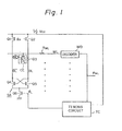
- Figure 1 shows an embodiment of the present invention, in which Ql and Q2 are transistors for precharging bit lines and are turned ON or OFF by a precharge clock signal ⁇ p.
- Q3 is a transistor for a word transfer gate of a memory cell CE, and C is a MOS capacitor.
- the memory cell CE is provided at each cross point between a word line WL and either one of a pair of bit lines BL and BL.
- the word line WL is driven by a word decoder WD.
- a sense amplifier SA is connected at the ends of the bit lines BL and BL.
- the sense amplifier SA has transistors Q4 and Q5 constructing a flip flop, and is activated by turning ON the transistor Q6 in response to an output signal ⁇ L from a timing circuit TC, as an embodiment of a detection circuit.
- a word line selecting signal ⁇ WL for driving the word decoder WD is input to the input of the timing circuit TC. Only a single word line WL and a single pair of bit lines are illustrated in Fig. 1, but, of course, a number of word lines and a number of pairs of bit lines are provided in practice.
- FIG. 2 shows a circuit diagram of the timing circuit TC in the circuit shown in Fig. 1.
- the timing circuit TC in Fig. 2 has n-channel transistors Q21 through Q29 and a time constant circuit constructed by a resistor R21 and a capacitor C21.
- the resistor R21 and the capacitor C21 are so determined that the time constant circuit has the same delay time as the delay time of the actually connected word line WL. That is, the delay time of the time constant circuit is not the estimated delay time of the longest possible delay, but is substantially the same as the delay time of the actually connected word line WL.
- This delay time of the delay circuit is realized by, for example, providing the same wiring pattern as the word line.
- the delay time may, of course, be realized by a resistor element and a capacitor element having the same resistance and capacitance as the word line WL and also having similar resistance and capacitance dependencies on process fluctuations as the word line WL. It is well known that such a-design technique will obtain a constant resistance or capacitance ratio among resistors or capacitors regardless of process variations, and accordingly, a detailed description thereof is omitted.
- the time constant circuit is provided at the input portion of the timing circuit TC, and the input of the time constant circuit is connected to the output signal 0W L of the word decoder.
- the output of the time constant circuit that is, a node Nl, is connected to the gate electrode of the transistor Q22.
- the timing circuit TC in the example shown in Fig.
- the transistors Q26 and Q27 are connected in series between Vcc and a node N4, which is a connecting point between the source of the transistor Q24 and the drain of the transistor Q25; the gate of the transistor Q26 is connected to a node N2, which is a connecting point between the source of the transistor Q21 and the drain of the transistor Q22; and the gates of the transistors Q27 and Q29 are connected to a node N3, which is a connecting point. between the source of the transistor Q23 and the drain of the transistor Q24.
- the transistors Q26 and Q27 form a positive feedback circuit.
- the output signal 0 L is obtained at a point between the source of the transistor Q28 and the drain of the transistor Q29.
- the reset clock signal ⁇ R is at a level higher than Vcc so that the transistors Q21 and Q23 are in an ON state. Therefore, the nodes N2 and N3 are charged up to the Vcc level, and accordingly, the transistors Q26 and Q27 are in the ON state, so that the node N4 is pulled up to a high level near the power supply level Vcc.
- the reset clock signal 0 R is pulled down to the Vss level so that the transistors Q21 and Q23 are turned OFF.
- the potentials at the nodes N2 and N3, however, remain at the Vcc level for a short time because charges remain at these nodes.
- the transistor Q22 remains in the OFF state until the word line selecting signal ⁇ WL applied through the delay circuit to the gate of the transistor Q22 reaches 1/2 Vcc + Vth, where Vth is the threshold voltage of the transistor Q22.
- the node N2 is at the high level Vcc so that the transistor Q26 remains in the ON state, and accordingly, the node N4 is charged up to a high level through the transistors Q26 and Q27.
- the potential at the node Nl gradually rises through the time constant circuit of R21 and C21. Even when a current begins to flow through the transistor Q25, because of the rise of the potential at the node N1, the potential at the node N4 is not suddenly lowered as long as the transistors Q22 and Q24 remain in the cut off state.
- the transistor Q22 turns ON only when the potential at the node N1 exceeds 1/2 Vcc + Vth, and the transistor Q24 turns ON only when the potential difference between the nodes Nl and N4 exceeds the threshold voltage Vth of the transistor Q24. Therefore, as long as the transistor Q24 is in the cut off state, the potential at the node N3 remains at the high level Vcc even when the potential at the node N4 is lowered to a certain extent.
- the transistor Q22 When the potential at the node Nl exceeds 1/2 Vcc + Vth, the transistor Q22 is turned ON so that the potential at the node N2 is lowered to 1/2 Vcc. This decreases the current flowing through the transistor Q26, resulting in a lowering of the potential at the node N4.
- the transistor Q24 In response to the lowered potential at the node N4, the transistor Q24 is turned ON so that a current flows through the transistors Q24 and Q25.
- the potential at the node N3 is lowered to the low level Vss, or the low level "L”, and in response to the lowered potential at the node N3, the transistor Q29 is turned OFF so that the output signal ⁇ L of the timing circuit TC becomes high level "H".
- the node N1 is so designed that the potential at the node Nl is the same as the potential at a point on the word line WL, and the potential rise time at that point is the longest of any point on the word line.
- the point having the longest rise time is the point farthest from the word decoder WD. Therefore, the transistor Q22 detects the potential at the point on the word line WL, and the potential rise time at that point is the longest at any point on the word line. That is, the turning ON of the transistor Q22 is not determined by an estimated time as in the previous type circuit, but is determined by the potential level at the node N1.
- a timing circuit TC a of another embodiment of the present invention is shown.
- the time constant circuit constructed by a resistor R31 and a capacitor C31 is the same as that of Fig. 2.
- the timing circuit TC a has p-channel MOS transistors Q31 and Q33 and n-channel MOS transistors Q32 and Q34.
- the transistors Q31 and Q32 are connected in series between the high voltage source Vcc and the precharge voltage source 1/2 Vcc, and the transistors Q33 and Q34 are connected between Vcc and Vss.
- the gate of the transistor Q31 receives a reset clock signal ⁇ R0
- the gate of the transistor Q34 receives another clock signal ⁇ R1 .
- the gate of the transistor Q32 is - connected to a node Nl, which is the output of the time constant circuit of R31 and C31, and the gate of the transistor Q33 is connected to a node N2 between the drain of the p-channel transistor Q31 and the drain of the n-channel transistor Q32.
- the reset clock signal ⁇ R0 applied to the gate the transistor Q31 is Vss
- the reset clock signal ⁇ R1 at the gate of the output transistor Q34 is Vcc. Therefore, the transistor Q31 is in an ON state so that the node N2 is at the Vcc level, and accordingly, the p-channel transistor Q33 is in the OFF state. Since the transistor Q34 is ON, the output signal ⁇ L of the detecting circuit is at the "L" level, i.e., at the reset level Vss.
- the reset clock signal ⁇ R0 is raised to Vcc and the reset clock signal ⁇ R1 is pulled down to Vss. Then the potential of the write clock signal ⁇ wL is raised to Vcc. This causes the potential at the node Nl to gradually rise with a delay by the time constant circuit including the resistor R31 and the capacitor C31.
- the transistor Q32 is turned ON so that the node N2 falls from Vcc to 1/2 Vcc.
- the p-channel transistor Q33 is turned ON. Since the reset clock signal ⁇ R1 is at the Vss level at this time, the transistor Q34 is in the OFF state. Therefore, the output signal ⁇ L rises to the Vcc level to activate the sense amplifier SA.
- the number of transistors is decreased in the timing circuit shown in Fig. 4 by employing p-channel transistors.
- a detection circuit TC b is provided at the point of the word line WL farthest from one of the decoders.
- the detection circuit TC b includes transistors Q61, Q62 and Q63.
- the drain of the transistor Q62 is connected to a node Nl.
- the transistor Q62 is connected between the high voltage source Vcc and the node Nl, and the gate of the transistor Q62 receives the precharge clock signal ⁇ P .
- the node Nl is connected to the gate of the.p-channel transistor Q63, and the source of the transistor Q63 is connected to the power supply line Vcc.
- the drain of the transistor Q63 is connected through a resistor R61 to the ground, and an output signal 0 L is obtained at a node N2 connected to the drain of the transistor Q63.
- the sense amplifier SA can be driven by the signal ⁇ L at the node N2.
- the timing circuit TC b a circuit can be used which is the same as the circuit shown in Fig. 2 or in Fig. 4 except that the time constant circuit is omitted.
- the word line potential is detected to activate the sense amplifier, it is not necessary to use an estimated time to take a time margin by considering the transmission variations of signals on the word line due to the word-line wiring resistance and other manufacturing variations, resulting in an improvement in the speed of a memory operation.
Landscapes
- Engineering & Computer Science (AREA)
- Microelectronics & Electronic Packaging (AREA)
- Dram (AREA)
- Read Only Memory (AREA)
- Static Random-Access Memory (AREA)
Applications Claiming Priority (2)
| Application Number | Priority Date | Filing Date | Title |
|---|---|---|---|
| JP61043084A JPS62202398A (ja) | 1986-02-28 | 1986-02-28 | 半導体記憶装置 |
| JP43084/86 | 1986-02-28 |
Publications (2)
| Publication Number | Publication Date |
|---|---|
| EP0240156A2 true EP0240156A2 (de) | 1987-10-07 |
| EP0240156A3 EP0240156A3 (de) | 1990-03-21 |
Family
ID=12653970
Family Applications (1)
| Application Number | Title | Priority Date | Filing Date |
|---|---|---|---|
| EP87301749A Withdrawn EP0240156A3 (de) | 1986-02-28 | 1987-02-27 | Halbleiterspeicheranordnung |
Country Status (4)
| Country | Link |
|---|---|
| US (1) | US4807193A (de) |
| EP (1) | EP0240156A3 (de) |
| JP (1) | JPS62202398A (de) |
| KR (1) | KR910002500B1 (de) |
Cited By (3)
| Publication number | Priority date | Publication date | Assignee | Title |
|---|---|---|---|---|
| WO1990007777A1 (en) * | 1988-12-24 | 1990-07-12 | Alcatel N.V. | Asynchronous timing circuit for a 2-coordinate memory |
| US5245584A (en) * | 1990-12-20 | 1993-09-14 | Vlsi Technology, Inc. | Method and apparatus for compensating for bit line delays in semiconductor memories |
| DE19525572A1 (de) * | 1994-07-15 | 1996-01-25 | Micron Technology Inc | Abfrageschaltung zum Verfolgen des Ladungstransfers duch Zugriffstransistoren in einem dynamischen Schreib-/Lese-Speicher |
Families Citing this family (5)
| Publication number | Priority date | Publication date | Assignee | Title |
|---|---|---|---|---|
| US4875191A (en) * | 1988-07-21 | 1989-10-17 | Intel Corporation | Integrated read and programming row driver |
| EP0915476B1 (de) * | 1997-11-05 | 2004-03-03 | STMicroelectronics S.r.l. | Verfahren und Schaltung zur Regulierung der Länge eines Adressenübergangssignals ATD |
| DE19842852B4 (de) | 1998-09-18 | 2005-05-19 | Infineon Technologies Ag | Integrierter Speicher |
| US7046566B1 (en) | 2004-12-06 | 2006-05-16 | Altera Corporation | Voltage-based timing control of memory bit lines |
| US9336862B2 (en) * | 2014-05-28 | 2016-05-10 | Oracle International Corporation | Sense amp activation according to word line common point |
Family Cites Families (6)
| Publication number | Priority date | Publication date | Assignee | Title |
|---|---|---|---|---|
| JPS54150064A (en) * | 1978-05-18 | 1979-11-24 | Toshiba Corp | Pulse generation circuit |
| JPS566072A (en) * | 1979-06-29 | 1981-01-22 | Nissan Motor Co Ltd | Ignition distributor |
| US4363111A (en) * | 1980-10-06 | 1982-12-07 | Heightley John D | Dummy cell arrangement for an MOS memory |
| JPS5838873B2 (ja) * | 1980-10-15 | 1983-08-25 | 富士通株式会社 | センス回路 |
| US4393475A (en) * | 1981-01-27 | 1983-07-12 | Texas Instruments Incorporated | Non-volatile semiconductor memory and the testing method for the same |
| JPS5987696A (ja) * | 1982-11-10 | 1984-05-21 | アドバンスト・マイクロ・デイバイシズ・インコ−ポレ−テツド | センス率の制御装置 |
-
1986
- 1986-02-28 JP JP61043084A patent/JPS62202398A/ja active Pending
-
1987
- 1987-02-25 US US07/018,559 patent/US4807193A/en not_active Expired - Fee Related
- 1987-02-27 EP EP87301749A patent/EP0240156A3/de not_active Withdrawn
- 1987-02-28 KR KR1019870001759A patent/KR910002500B1/ko not_active Expired
Cited By (5)
| Publication number | Priority date | Publication date | Assignee | Title |
|---|---|---|---|---|
| WO1990007777A1 (en) * | 1988-12-24 | 1990-07-12 | Alcatel N.V. | Asynchronous timing circuit for a 2-coordinate memory |
| US5170376A (en) * | 1988-12-24 | 1992-12-08 | Alcatel N.V. | Asynchronous timing circuit for a 2-coordinate memory |
| US5245584A (en) * | 1990-12-20 | 1993-09-14 | Vlsi Technology, Inc. | Method and apparatus for compensating for bit line delays in semiconductor memories |
| DE19525572A1 (de) * | 1994-07-15 | 1996-01-25 | Micron Technology Inc | Abfrageschaltung zum Verfolgen des Ladungstransfers duch Zugriffstransistoren in einem dynamischen Schreib-/Lese-Speicher |
| DE19525572C2 (de) * | 1994-07-15 | 1998-06-04 | Micron Technology Inc | Abfrageschaltung zum Verfolgen des Ladungstransfers duch Zugriffstransistoren in einem dynamischen Schreib-/Lese-Speicher |
Also Published As
| Publication number | Publication date |
|---|---|
| KR910002500B1 (ko) | 1991-04-23 |
| US4807193A (en) | 1989-02-21 |
| KR870008321A (ko) | 1987-09-25 |
| EP0240156A3 (de) | 1990-03-21 |
| JPS62202398A (ja) | 1987-09-07 |
Similar Documents
| Publication | Publication Date | Title |
|---|---|---|
| US5764562A (en) | Semiconductor memory device | |
| KR100239958B1 (ko) | 반도체 기억장치 | |
| US6504761B2 (en) | Non-volatile semiconductor memory device improved sense amplification configuration | |
| JP3101298B2 (ja) | 半導体メモリ装置 | |
| KR930014588A (ko) | 반도체 기억장치 | |
| US4733112A (en) | Sense amplifier for a semiconductor memory device | |
| US5323345A (en) | Semiconductor memory device having read/write circuitry | |
| US4539661A (en) | Static-type semiconductor memory device | |
| US4578781A (en) | MIS transistor circuit | |
| US4807193A (en) | Semiconductor memory device with a detection circuit to detect word line potential | |
| US4760559A (en) | Semiconductor memory device | |
| EP1776704B1 (de) | Wortleitungssteuerungsschaltung zur verbesserung der dynamischen auffrischung in einer halbleiterspeichervorrichtung mit reduzierter standby-stromversorgung | |
| US6067264A (en) | High speed semiconductor memory device | |
| USRE36159E (en) | Semiconductor integrated circuit device having built-in voltage drop circuit | |
| US5777934A (en) | Semiconductor memory device with variable plate voltage generator | |
| JPS6376192A (ja) | 半導体記憶装置 | |
| US5365488A (en) | Data reading circuit having a clamping circuit for clamping a pair of data buses to predetermined potentials | |
| US5594681A (en) | Dynamic random access memory wherein timing of completion of data reading is advanced | |
| KR100443100B1 (ko) | 제어된오버드라이브회로를갖는반도체집적회로장치 | |
| US5973987A (en) | Semiconductor memory device delaying ATD pulse signal to generate word line activation signal | |
| US5553032A (en) | Dynamic random access memory wherein timing of completion of data reading is advanced | |
| EP0350860A2 (de) | Halbleiterspeicher mit verbesserten Abfühlverstärkern | |
| KR100335118B1 (ko) | 메모리 소자의 구동 회로 | |
| JPH02154394A (ja) | 半導体メモリ装置 | |
| JP5292661B2 (ja) | 半導体記憶装置 |
Legal Events
| Date | Code | Title | Description |
|---|---|---|---|
| PUAI | Public reference made under article 153(3) epc to a published international application that has entered the european phase |
Free format text: ORIGINAL CODE: 0009012 |
|
| AK | Designated contracting states |
Kind code of ref document: A2 Designated state(s): DE FR GB |
|
| PUAL | Search report despatched |
Free format text: ORIGINAL CODE: 0009013 |
|
| AK | Designated contracting states |
Kind code of ref document: A3 Designated state(s): DE FR GB |
|
| 17P | Request for examination filed |
Effective date: 19900711 |
|
| 17Q | First examination report despatched |
Effective date: 19910809 |
|
| RBV | Designated contracting states (corrected) |
Designated state(s): FR |
|
| REG | Reference to a national code |
Ref country code: DE Ref legal event code: 8566 |
|
| STAA | Information on the status of an ep patent application or granted ep patent |
Free format text: STATUS: THE APPLICATION IS DEEMED TO BE WITHDRAWN |
|
| 18D | Application deemed to be withdrawn |
Effective date: 19940829 |
|
| RIN1 | Information on inventor provided before grant (corrected) |
Inventor name: SATO, KIMIAKI Inventor name: HORII, TAKASHI Inventor name: TAKADA, YASUHIRO Inventor name: KODAMA, NOBUMI Inventor name: TAKEMAE, YOSHIHIRO Inventor name: YANAGISAWA, MAKOTO Inventor name: TATEMATSU, TAKEO |