EP0237322B1 - Bascule de verrouillage - Google Patents
Bascule de verrouillage Download PDFInfo
- Publication number
- EP0237322B1 EP0237322B1 EP87302040A EP87302040A EP0237322B1 EP 0237322 B1 EP0237322 B1 EP 0237322B1 EP 87302040 A EP87302040 A EP 87302040A EP 87302040 A EP87302040 A EP 87302040A EP 0237322 B1 EP0237322 B1 EP 0237322B1
- Authority
- EP
- European Patent Office
- Prior art keywords
- gate
- emitter
- power source
- transistor
- inverted
- Prior art date
- Legal status (The legal status is an assumption and is not a legal conclusion. Google has not performed a legal analysis and makes no representation as to the accuracy of the status listed.)
- Expired - Lifetime
Links
Images


Classifications
-
- G—PHYSICS
- G11—INFORMATION STORAGE
- G11C—STATIC STORES
- G11C11/00—Digital stores characterised by the use of particular electric or magnetic storage elements; Storage elements therefor
- G11C11/21—Digital stores characterised by the use of particular electric or magnetic storage elements; Storage elements therefor using electric elements
- G11C11/34—Digital stores characterised by the use of particular electric or magnetic storage elements; Storage elements therefor using electric elements using semiconductor devices
-
- H—ELECTRICITY
- H03—ELECTRONIC CIRCUITRY
- H03K—PULSE TECHNIQUE
- H03K3/00—Circuits for generating electric pulses; Monostable, bistable or multistable circuits
- H03K3/02—Generators characterised by the type of circuit or by the means used for producing pulses
- H03K3/26—Generators characterised by the type of circuit or by the means used for producing pulses by the use, as active elements, of bipolar transistors with internal or external positive feedback
- H03K3/28—Generators characterised by the type of circuit or by the means used for producing pulses by the use, as active elements, of bipolar transistors with internal or external positive feedback using means other than a transformer for feedback
- H03K3/281—Generators characterised by the type of circuit or by the means used for producing pulses by the use, as active elements, of bipolar transistors with internal or external positive feedback using means other than a transformer for feedback using at least two transistors so coupled that the input of one is derived from the output of another, e.g. multivibrator
- H03K3/286—Generators characterised by the type of circuit or by the means used for producing pulses by the use, as active elements, of bipolar transistors with internal or external positive feedback using means other than a transformer for feedback using at least two transistors so coupled that the input of one is derived from the output of another, e.g. multivibrator bistable
- H03K3/288—Generators characterised by the type of circuit or by the means used for producing pulses by the use, as active elements, of bipolar transistors with internal or external positive feedback using means other than a transformer for feedback using at least two transistors so coupled that the input of one is derived from the output of another, e.g. multivibrator bistable using additional transistors in the input circuit
- H03K3/2885—Generators characterised by the type of circuit or by the means used for producing pulses by the use, as active elements, of bipolar transistors with internal or external positive feedback using means other than a transformer for feedback using at least two transistors so coupled that the input of one is derived from the output of another, e.g. multivibrator bistable using additional transistors in the input circuit the input circuit having a differential configuration
-
- H—ELECTRICITY
- H03—ELECTRONIC CIRCUITRY
- H03K—PULSE TECHNIQUE
- H03K3/00—Circuits for generating electric pulses; Monostable, bistable or multistable circuits
- H03K3/02—Generators characterised by the type of circuit or by the means used for producing pulses
- H03K3/027—Generators characterised by the type of circuit or by the means used for producing pulses by the use of logic circuits, with internal or external positive feedback
- H03K3/037—Bistable circuits
- H03K3/0375—Bistable circuits provided with means for increasing reliability; for protection; for ensuring a predetermined initial state when the supply voltage has been applied; for storing the actual state when the supply voltage fails
-
- H—ELECTRICITY
- H03—ELECTRONIC CIRCUITRY
- H03K—PULSE TECHNIQUE
- H03K3/00—Circuits for generating electric pulses; Monostable, bistable or multistable circuits
- H03K3/02—Generators characterised by the type of circuit or by the means used for producing pulses
- H03K3/37—Generators characterised by the type of circuit or by the means used for producing pulses by the use, as active elements, of gas-filled tubes, e.g. astable trigger circuits
Definitions
- the present invention relates to a latch circuit.
- latch circuits such as a delay (D) type flip-flop (FF) or a set-reset (R-S) type FF. These latch circuits have hold loops to feedback either a normal output Q or an inverted output Q , and to hold the status latched therein.
- D delay
- R-S set-reset
- latch circuits have hold loops to feedback either a normal output Q or an inverted output Q , and to hold the status latched therein.
- each latch circuit has only a single hold loop. Consequently, this type of latch circuit is easily caused to malfunction by instantaneous electrical noise, such as noise due to alpha-ray exposure. This will be described in more detail with reference to specific examples.
- First and second hold lines supply the complementary latch outputs to the second gate circuit.
- the second gate circuit consists of an emitter-coupled pair of transistors whose bases are supplied with the latch output via respective "hold lines" in the form of emitter follower circuits
- the third gate circuit consists of an independent pair of emitter follower circuits.
- EP-A-0 167 339 by Sony Corporation discloses various ECL logic circuits in which the need for a reference voltage is avoided by using two voltage levels to represent logic "L” and two voltage levels to represent logic "H".
- first to third gate circuits are arranged to form an R-S flip-flop provided with a single hold line for supplying a latch output to the second gate circuit.
- DE-B-1 230 079 discloses a bistable multivibrator (latch) having an emitter-coupled transistor pair which is cross-coupled via two emitter followers.
- the emitter followers apparently act like hold loops although this document does not address the problem of noise due to alpha-ray exposure.
- the circuit of Fig. 3 includes, in addition to the basic multivibrator circuit, set and reset gates for setting and resetting the multivibrator in response to a clock signal.
- a special feature of this circuit is that the latching transistors of the emitter-coupled pair are precharged by means of voltage dividers, so that the input voltage needed to switch the latching transistors is half the sum of their base and emitter voltages.
- An embodiment of the present invention may provide a latch circuit having a remarkably improved noise tolerance.
- An embodiment of the present invention may provide a latch circuit having a simple circuit configuration.
- a latch circuit comprising a first gate connected to receive data and a clock signal, a second gate connected to receive an inverted clock signal, and a third gate operatively connected to output terminals of said first and second gates, a first hold line being provided between an inverted output terminal of said third gate and a third input terminal of said second gate, and a second hold line being provided between a non-inverted output terminal of said third gate and an inverted input terminal of said second gate;
- said first gate is formed by an emitter-coupled logic gate circuit consisting of first to third emitter-coupled transistors whose coupled emitters are connected to a second power source via a current source, resistors connecting collectors of said first to third transistors to a first power source, a first output transistor having a base connected to the collectors of said first and second transistors and a collector connected to said first power source, and a resistor connecting an emitter of said first output transistor to said second power source;
- said second gate is formed by an emitter-coupled logic gate circuit consisting of
- an "in-phase" hold type latch circuit of the prior art consists of a first OR gate G1 receiving a data D and a clock signal CL and outputting an inverted output SQ and a non-inverted internal output, a second OR gate G2 receiving an inverted clock signal CL at an input terminal thereof and outputting an inverted output connected to the inverted output SQ from the OR gate G1 and a non-inverted internal output, and a wired-AND gate G3 receiving the non-inverted internal outputs from the OR gates G1 and G2 and outputting a non-inverted (normal) output SQ.
- a hold line HL is provided between an output terminal of the wired-AND gate G3 and another input terminal of the OR gate G2.
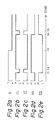
- the operation of the latch circuit in Fig. 1 will be described with reference to Figs. 2a to 2e.
- the basic operation of the latch circuit is that the data D is latched in response to the trailing of the clock signal CL.
- a time t1 when the clock signal CL is changed from a high level "H” to a low level “L” a high level “H” of the data D is taken in the latch circuit.
- the OR gate G1 outputs a low level signal at the inverted output terminal and a high level signal at the non-inverted output terminal.
- the inverted output of the OR gate G2 becomes low level, because the inverted clock signal CL applied to the OR gate G2 is at a high level.
- the inverted output SQ of the latch circuit becomes low level.
- the AND gate G3 outputs a high level non-inverted output SQ.
- the clock signal CL is restored to a high level "H” from a low level "L"
- the OR gate G1 still outputs a high level signal at the non-inverted output terminal
- the AND gate G3 still outputs the high level non-inverted output SQ.
- a low level “L” of the data D is taken in the latch circuit.
- the OR gate G1 outputs a high level signal at the inverted output terminal and a low level signal at the non-inverted output terminal, and the AND gate G3 outputs a low level signal. That is, the non-inverted output SQ of the latch circuit is changed to a low level.
- the output signals from the inverted output terminals of the OR gate G1 and G2 are high level, and thus the inverted output SQ of the latch circuit is changed to a high level.
- the OR gate G2 outputs a high level signal at the inverted output terminal and a low level signal at the non-inverted output terminal.
- the output of the AND gate G3 becomes low level, and as a result, a low level of the non-inverted output SQ and a high level of the inverted output SQ are maintained.
- the hold loop HL has the above data latch function.
- a transistor connected to the hold line HL is exposed to alpha-rays when the non-inverted output SQ, i.e., the feedback signal on the hold line HL, is high, a voltage at a collector of the transistor, i.e., a voltage of the feedback signal on the hold line HL, may fall in a short period due to the above phenomenon. If the level of the voltage on the hold line HL becomes lower than a threshold level V TH of a transistor in, for example, the OR gate G2, the OR gate G2 may output a low level signal from the non-inverted output terminal thereof in a short time.
- the output SQ may be changed to a low level, and the feedback signal on the hold line HL also may be changed to a low level.
- the inverted output SQ of the latch circuit is changed to a high level. This means that the latch circuit in Fig. 1 will malfunction due to the noise of the alpha-rays.
- an "inverted phase" hold type latch circuit of the prior art consists of two NOR gates G5 and G6, and an OR gate G4.
- the NOR gate G6 receives the data D and the clock signal CL
- the NOR gate G5 receives the inverted clock signal CL .
- a hold line HL is provided between an inverted output terminal of the OR gate G4 and an input terminal of the NOR gate G5.
- the OR gate G4 outputs an inverted output SQ and a non-inverted output SQ.
- the operation of the latch circuit in Fig. 3 is the same as that of the latch circuit in Fig. 1, as described with reference to Figs. 2a to 2e, and thus a description thereof is omitted.
- the latch circuit of Fig. 3 also suffers from the disadvantage of a malfunction due to noise .
- the latch circuit in Fig. 4 is a so-called "inverted phase" hold type latch circuit and corresponds to the latch circuit of Fig. 3.
- the latch circuit of Fig. 4 includes a first NOR gate G16 receiving data D and a clock signal CL, a second NOR gate G15 receiving an inverted clock signal CL , and an OR gate G14.
- the latch circuit is provided with two hold lines HL1 and HL2.
- the hold line HL1 is provided between an inverted output terminal of the OR gate G14 and a third input terminal of the NOR gate G15, and the hold line HL2 is provided between a non-inverted output terminal of the OR gate G14 and an inverted input terminal of the NOR gate G15.
- a signal on the hold line HL1 has an inverted phase relationship to a signal on the hold line HL2.
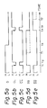
- the data D is at a high level "H” and the clock signal CL is changed to a low level “L”, and accordingly, the NOR gate G16 outputs a signal S16 having a low level "L".
- the NOR gate G15 receives the inverted clock signal CL having a high level "H” and outputs an signal S15 having a low level "L”.
- the OR gate G14 outputs a non-inverted output SQ having a high level "H” at an inverted output terminal and an inverted output SQ having a low level "L” at another output terminal.
- a signal having a high level on the hold line HL1 and/or a signal having a low level on the hold line HL2 ensure that a low level of the signal S15 from the NOR gate G15 is maintained when the clock signal CL is restored to a high level and the inverted clock signal CL is also restored to a low level at the time t2.
- the data D is a low level "L” and the clock signal CL is again changed to a low level "L", then the NOR gate G16 outputs the signal S16 having a high level "H”.
- the OR gate G14 receiving the signal S16 having a high level outputs the inverted output SQ having a high level and the non-inverted output SQ having a low level.
- the clock signal CL is restored to a high level, and accordingly, the signal S16 from the NOR gate G16 is changed to a low level "L".
- the inverted clock signal CL having a low level, the inverted output SQ having a high level to the inverted input terminal of the NOR gate G15 and the non-inverted output SQ having a low level are supplied to the NOR gate G15, and the signal S15 having a high level is output, and the output status of the outputs SQ and SQ is maintained.
- the OR gate G14, the NOR gate G15, and the hold lines HL1 and HL2 form a set-reset (R-S) type flip-flop.
- the NOR gate G16 provides a reset signal R, and the inverted clock signal CL supplied to the NOR gate G15 corresponds to a set signal S.
- the provision of the inverted input terminal at the NOR gate G15 for directly receiving an additional feedback signal on the hold line HL2 results in a greater noise margin than that of the latch circuit using an inverter INV as shown by dotted line.
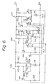
- the "inverted-phase" hold type latch circuit includes the NOR gate G16 formed by an ECL gate circuit consisting of transistors Q32, Q33, and Q34, a current source I16 and resistors R21 and R22, an output transistor Q31 and a resistor R23, the OR gate G14 formed by an ECL gate circuit consisting of transistors Q11, Q12, and Q13, a current resistor I14 and resistors R11 and R12, output transistors Q14 and Q15, and resistors R13 and R14, and the NOR gate G15 formed by an ECL gate circuit consisting of transistors Q16, Q17, and Q18, a current source I15 and resistors R15 and R16, 97 output transistor Q19, and a resistor R17.
- the latch circuit is supplied with the first and second power sources V CC and V EE .
- the data D is supplied to a base of the transistor Q32, and the clock signal CL is supplied to a base of the transistor Q33.
- the inverted clock signal CL is supplied to a base of the transistor Q17.
- a base of the transistor Q11 is supplied with a signal from an emitter of the transistor Q19, and a base of the transistor Q12 is supplied with a signal from an emitter of the transistor Q31.
- the base of the transistors Q34 and Q13 are supplied with the reference voltage Vref.
- the first hold line HL1 is provided between an emitter of the transistor Q14 and a base of the transistor Q16
- the second hold line HL2 is provided between an emitter of the transistor Q15 and a base of the transistor Q18.
- the signals on the hold lines HL1 and HL2 have inverted polarities.
- feedback signals i.e., the signals from the transistors Q14 and Q15, are directly supplied to the bases of the transistors Q16 and Q18 without providing an inverter. This also results in a high noise tolerance and a simple circuit configuration.
- the latch circuit may operate as a set-reset type flip-flop. The operation is shown in Table 1.
Landscapes
- Engineering & Computer Science (AREA)
- Power Engineering (AREA)
- Computer Hardware Design (AREA)
- Logic Circuits (AREA)
- Shift Register Type Memory (AREA)
Claims (1)
- Bascule de verrouillage comprenant une première porte (G16) reliée afin de recevoir un signal de données (D) et un signal d'horloge (CL), une seconde porte (G15) reliée afin de recevoir un signal d'horloge inversé (CL), et une troisième porte (G14) reliée fonctionnellement aux bornes de sortie des dites première et seconde portes, une première ligne de maintien (HL1) étant placée entre une borne de sortie inversée de ladite troisième porte (G14) et une troisième borne d'entrée de ladite seconde porte (G15), et une seconde ligne de maintien (HL2) étant placée entre une borne de sortie non-inversée de ladite troisième porte (G14) et une borne d'entrée inversée de ladite seconde porte (G15); dans laquelle:
ladite première porte (G16) est formée par un circuit logique ECL à couplage par les émetteurs se composant des premier au troisième transistors à couplage par les émetteurs (Q32, Q33, Q34) dont les émetteurs couplés sont reliés à une seconde source de tension (VEE) via une source de courant (I16), des résistances (R21, R22) reliant les collecteurs desdits premier au troisième transistors (Q32, Q33, Q34) à une première source de tension (VCC), un premier transistor de sortie (Q31) ayant la base reliée aux collecteurs desdits premier et second transistors (Q32, Q33) et le collecteur relié à ladite première source de tension (VCC), et une résistance (R23) reliant l'émetteur dudit premier transistor de sortie (Q31) à ladite seconde source de tension (VEE);
ladite seconde porte (G15) est formée par un circuit logique ECL à couplage par les émetteurs des quatrième au sixième transistors à couplage par les émetteurs (Q16, Q17, Q18) dont les émetteurs couplés sont reliés à une seconde source de tension (VEE) via une source de courant (I15), des résistances (R15, R16) reliant les collecteurs desdits quatrième au sixième transistors (Q16, Q17, Q18) à ladite première source de tension (VCC), un second transistor de sortie (Q19) ayant la base reliée auxdits collecteurs desdits quatrième et cinquième transistors (Q16, Q17) et le collecteur relié à ladite première source de tension (VCC), et une résistance (R17) reliant l'émetteur dudit second transistor de sortie (Q19) à ladite seconde source de tension (VEE); et
ladite troisième porte (G14) est formée par un circuit logique ECL à couplage par les émetteurs se composant des septième au neuvième transistors à couplage par les émetteurs (Q11, Q12, Q13) dont les émetteurs couplés sont reliés à une seconde source de tension (VEE) via une source de courant constant (I14) et des résistances (R11, R12) reliant les collecteurs desdits septième au huitième transistors (Q11, Q12, Q13) à ladite première source de tension (VCC), un troisième transistor de sortie (Q14) ayant la base reliée auxdits collecteurs desdits septième et neuvième transistors (Q11, Q12), le collecteur relié à ladite première source de tension (VCC), et l'émetteur relié via une résistance (R13) à ladite seconde source de tension (VEE), un quatrième transistor de sortie (Q15) ayant la base reliée audit collecteur dudit neuvième transistor (Q13) et le collecteur relié à ladite première source de tension (VCC), et une résistance (R14) reliant l'émetteur dudit quatrième transistor de sortie (Q15) à ladite seconde source de tension (VEE); dans laquelle:
ladite première ligne de maintien (HL1) est placée entre l'émetteur dudit troisième transistor de sortie (Q14) et la base dudit quatrième transistor (Q16);
ladite seconde ligne de maintien (HL2) est placée entre l'émetteur dudit quatrième transistor de sortie (Q15) et la base dudit sixième transistor de sortie (Q18);
l'émetteur dudit premier transistor de sortie (Q31) et la base dudit huitième transistor (Q12) sont généralement reliés; et
l'émetteur dudit second transistor de sortie (Q19) et la base dudit septième transistor (Q11) sont généralement reliés.
Applications Claiming Priority (2)
| Application Number | Priority Date | Filing Date | Title |
|---|---|---|---|
| JP61051369A JPS62222711A (ja) | 1986-03-11 | 1986-03-11 | ラツチ回路 |
| JP51369/86 | 1986-03-11 |
Related Child Applications (1)
| Application Number | Title | Priority Date | Filing Date |
|---|---|---|---|
| EP92114729.4 Division-Into | 1987-03-10 |
Publications (3)
| Publication Number | Publication Date |
|---|---|
| EP0237322A2 EP0237322A2 (fr) | 1987-09-16 |
| EP0237322A3 EP0237322A3 (en) | 1989-07-05 |
| EP0237322B1 true EP0237322B1 (fr) | 1993-08-18 |
Family
ID=12885025
Family Applications (2)
| Application Number | Title | Priority Date | Filing Date |
|---|---|---|---|
| EP87302040A Expired - Lifetime EP0237322B1 (fr) | 1986-03-11 | 1987-03-10 | Bascule de verrouillage |
| EP92114729A Withdrawn EP0523747A1 (fr) | 1986-03-11 | 1987-03-10 | Bascule de verrouillage |
Family Applications After (1)
| Application Number | Title | Priority Date | Filing Date |
|---|---|---|---|
| EP92114729A Withdrawn EP0523747A1 (fr) | 1986-03-11 | 1987-03-10 | Bascule de verrouillage |
Country Status (5)
| Country | Link |
|---|---|
| US (1) | US4779011A (fr) |
| EP (2) | EP0237322B1 (fr) |
| JP (1) | JPS62222711A (fr) |
| KR (1) | KR900004570B1 (fr) |
| DE (1) | DE3787037T2 (fr) |
Families Citing this family (5)
| Publication number | Priority date | Publication date | Assignee | Title |
|---|---|---|---|---|
| US5091659A (en) * | 1991-04-16 | 1992-02-25 | International Business Machines Corporation | Composite logic gate circuit with means to reduce voltage required by logic transistors from external source |
| JP3135300B2 (ja) * | 1991-08-20 | 2001-02-13 | 沖電気工業株式会社 | ラッチ回路 |
| US7495493B2 (en) * | 2006-08-30 | 2009-02-24 | Freescale Semiconductor, Inc. | Circuitry for latching |
| JP5807333B2 (ja) * | 2011-01-27 | 2015-11-10 | ソニー株式会社 | ディレイラッチ回路、および、ディレイフリップフロップ |
| JP2014060669A (ja) * | 2012-09-19 | 2014-04-03 | Fujitsu Ltd | マスタスレーブ型フリップフロップ回路 |
Citations (2)
| Publication number | Priority date | Publication date | Assignee | Title |
|---|---|---|---|---|
| DE1230079B (de) * | 1964-04-30 | 1966-12-08 | Motorola Inc | Bistabiler Multivibrator mit Emitteranzapfung |
| EP0167339A2 (fr) * | 1984-06-30 | 1986-01-08 | Sony Corporation | Circuit logique |
Family Cites Families (23)
| Publication number | Priority date | Publication date | Assignee | Title |
|---|---|---|---|---|
| US3178590A (en) * | 1962-04-02 | 1965-04-13 | Ibm | Multistate memory circuit employing at least three logic elements |
| US3339089A (en) * | 1965-05-11 | 1967-08-29 | Rca Corp | Electrical circuit |
| US3427470A (en) * | 1965-08-11 | 1969-02-11 | Mohawk Data Sciences Corp | Multiple level logic circuits |
| DE1941264C3 (de) * | 1969-08-13 | 1975-07-17 | Siemens Ag, 1000 Berlin Und 8000 Muenchen | Asynchrone RS-Kippstufe in ECL-Technik |
| US3728560A (en) * | 1971-01-29 | 1973-04-17 | Motorola Inc | Bistable multivibrator circuit |
| GB1484946A (en) * | 1973-09-13 | 1977-09-08 | Naigai Ind Inc | Logic circuit equivalent to a relay contact circuit |
| DE2460644C3 (de) * | 1974-10-30 | 1982-01-28 | Siemens AG, 1000 Berlin und 8000 München | Basisgekoppelte Flipflops |
| JPS5284938A (en) * | 1976-01-07 | 1977-07-14 | Hitachi Ltd | Logic circuit |
| DE2723386C3 (de) * | 1976-06-01 | 1981-08-13 | Motorola, Inc., 60196 Schaumburg, Ill. | Logik Schaltungsanordnung |
| US4045693A (en) * | 1976-07-08 | 1977-08-30 | Gte Automatic Electric Laboratories Incorporated | Negative r-s triggered latch |
| JPS566535A (en) * | 1979-06-28 | 1981-01-23 | Nec Corp | Integrated circuit |
| JPS56156026A (en) * | 1980-05-02 | 1981-12-02 | Hitachi Ltd | Composite logical circuit |
| GB2121573B (en) * | 1980-07-11 | 1984-12-19 | Fairchild Camera Instr Co | Programmable logic array circuit |
| US4378505A (en) * | 1980-09-29 | 1983-03-29 | Bell Telephone Laboratories, Inc. | Emitter function logic latch and counter circuits |
| JPS5883434A (ja) * | 1981-11-13 | 1983-05-19 | Hitachi Ltd | 半導体集積回路装置 |
| US4459683A (en) * | 1982-04-14 | 1984-07-10 | Signetics Corporation | Read resettable memory circuit |
| US4439690A (en) * | 1982-04-26 | 1984-03-27 | International Business Machines Corporation | Three-gate hazard-free polarity hold latch |
| US4540900A (en) * | 1982-07-01 | 1985-09-10 | Burr-Brown Corporation | Reduced swing latch circuit utilizing gate current proportional to temperature |
| EP0098891B1 (fr) * | 1982-07-13 | 1986-01-29 | Ibm Deutschland Gmbh | Diviseur de phase avec circuit de verrouillage intégré |
| JPS5981921A (ja) * | 1982-11-01 | 1984-05-11 | Hitachi Ltd | 高速論理回路 |
| JPS6051323A (ja) * | 1983-08-31 | 1985-03-22 | Toshiba Corp | Cmos伝送回路 |
| US4675553A (en) * | 1984-03-12 | 1987-06-23 | Amdahl Corporation | Sequential logic circuits implemented with inverter function logic |
| JPH0691428B2 (ja) * | 1985-01-23 | 1994-11-14 | 株式会社日立製作所 | フリツプフロツプ回路 |
-
1986
- 1986-03-11 JP JP61051369A patent/JPS62222711A/ja active Granted
-
1987
- 1987-03-09 KR KR8702079A patent/KR900004570B1/ko not_active IP Right Cessation
- 1987-03-10 DE DE87302040T patent/DE3787037T2/de not_active Expired - Fee Related
- 1987-03-10 EP EP87302040A patent/EP0237322B1/fr not_active Expired - Lifetime
- 1987-03-10 EP EP92114729A patent/EP0523747A1/fr not_active Withdrawn
- 1987-03-11 US US07/024,717 patent/US4779011A/en not_active Expired - Fee Related
Patent Citations (2)
| Publication number | Priority date | Publication date | Assignee | Title |
|---|---|---|---|---|
| DE1230079B (de) * | 1964-04-30 | 1966-12-08 | Motorola Inc | Bistabiler Multivibrator mit Emitteranzapfung |
| EP0167339A2 (fr) * | 1984-06-30 | 1986-01-08 | Sony Corporation | Circuit logique |
Non-Patent Citations (1)
| Title |
|---|
| A.H. Seidman, "Integrated Circuits Applications Handbook", John Wiley & Sons, New York, 1983, page 82 * |
Also Published As
| Publication number | Publication date |
|---|---|
| EP0237322A3 (en) | 1989-07-05 |
| JPH0453449B2 (fr) | 1992-08-26 |
| KR870009382A (ko) | 1987-10-26 |
| DE3787037T2 (de) | 1993-12-09 |
| US4779011A (en) | 1988-10-18 |
| DE3787037D1 (de) | 1993-09-23 |
| EP0237322A2 (fr) | 1987-09-16 |
| EP0523747A1 (fr) | 1993-01-20 |
| KR900004570B1 (en) | 1990-06-29 |
| JPS62222711A (ja) | 1987-09-30 |
Similar Documents
| Publication | Publication Date | Title |
|---|---|---|
| US4628216A (en) | Merging of logic function circuits to ECL latch or flip-flop circuit | |
| US4560888A (en) | High-speed ECL synchronous logic circuit with an input logic circuit | |
| US4755693A (en) | ECL latch circuit insensitive to alpha ray disturbances | |
| US4622475A (en) | Data storage element having input and output ports isolated from regenerative circuit | |
| GB1367205A (en) | Ternary logic circuits | |
| US5099142A (en) | Trigger circuit with switching hysteresis | |
| EP0237322B1 (fr) | Bascule de verrouillage | |
| US4359647A (en) | Master-slave flip-flop arrangement | |
| US4639661A (en) | Power-down arrangement for an ECL circuit | |
| KR100220440B1 (ko) | Ecl 레벨용 입력 버퍼 재생 래치 회로 | |
| US5250860A (en) | Three-level cascode differential current switch | |
| US4349753A (en) | Emitter function logic flip-flop circuit | |
| JP2887898B2 (ja) | ラッチ回路 | |
| US4868420A (en) | Flip-flop circuit | |
| US4810900A (en) | ECL circuit with improved α-ray resistant properties | |
| US4578599A (en) | Flip-flop having improved synchronous reset | |
| US4749885A (en) | Nonsaturating bipolar logic gate having a low number of components and low power dissipation | |
| US5015874A (en) | Status holding circuit and logic circuit using the same | |
| US4277698A (en) | Delay type flip-flop | |
| JP2933022B2 (ja) | フリップフロップ回路 | |
| JPH0236610A (ja) | マスタースレーブ型dタイプフリップフロップ回路 | |
| US5541545A (en) | High speed bipolar D latch circuit with reduced latch clocking output corruption | |
| JPS60142619A (ja) | 半導体集積回路 | |
| JPS6316047B2 (fr) | ||
| SU1185578A1 (ru) | @ К-триггер |
Legal Events
| Date | Code | Title | Description |
|---|---|---|---|
| PUAI | Public reference made under article 153(3) epc to a published international application that has entered the european phase |
Free format text: ORIGINAL CODE: 0009012 |
|
| AK | Designated contracting states |
Kind code of ref document: A2 Designated state(s): DE FR GB |
|
| PUAL | Search report despatched |
Free format text: ORIGINAL CODE: 0009013 |
|
| AK | Designated contracting states |
Kind code of ref document: A3 Designated state(s): DE FR GB |
|
| RHK1 | Main classification (correction) |
Ipc: H03K 19/20 |
|
| 17P | Request for examination filed |
Effective date: 19890721 |
|
| 17Q | First examination report despatched |
Effective date: 19900926 |
|
| GRAA | (expected) grant |
Free format text: ORIGINAL CODE: 0009210 |
|
| AK | Designated contracting states |
Kind code of ref document: B1 Designated state(s): DE FR GB |
|
| XX | Miscellaneous (additional remarks) |
Free format text: TEILANMELDUNG 92114729.4 EINGEREICHT AM 18/03/87. |
|
| REF | Corresponds to: |
Ref document number: 3787037 Country of ref document: DE Date of ref document: 19930923 |
|
| ET | Fr: translation filed | ||
| PLBE | No opposition filed within time limit |
Free format text: ORIGINAL CODE: 0009261 |
|
| STAA | Information on the status of an ep patent application or granted ep patent |
Free format text: STATUS: NO OPPOSITION FILED WITHIN TIME LIMIT |
|
| 26N | No opposition filed | ||
| PGFP | Annual fee paid to national office [announced via postgrant information from national office to epo] |
Ref country code: GB Payment date: 19980302 Year of fee payment: 12 |
|
| PGFP | Annual fee paid to national office [announced via postgrant information from national office to epo] |
Ref country code: FR Payment date: 19980310 Year of fee payment: 12 |
|
| PGFP | Annual fee paid to national office [announced via postgrant information from national office to epo] |
Ref country code: DE Payment date: 19980313 Year of fee payment: 12 |
|
| PG25 | Lapsed in a contracting state [announced via postgrant information from national office to epo] |
Ref country code: GB Free format text: LAPSE BECAUSE OF NON-PAYMENT OF DUE FEES Effective date: 19990310 |
|
| GBPC | Gb: european patent ceased through non-payment of renewal fee |
Effective date: 19990310 |
|
| PG25 | Lapsed in a contracting state [announced via postgrant information from national office to epo] |
Ref country code: FR Free format text: LAPSE BECAUSE OF NON-PAYMENT OF DUE FEES Effective date: 19991130 |
|
| REG | Reference to a national code |
Ref country code: FR Ref legal event code: ST |
|
| PG25 | Lapsed in a contracting state [announced via postgrant information from national office to epo] |
Ref country code: DE Free format text: LAPSE BECAUSE OF NON-PAYMENT OF DUE FEES Effective date: 20000101 |