EP0236956B1 - Circuit pour la compensation numérique d'un signal perturbateur déterminé - Google Patents
Circuit pour la compensation numérique d'un signal perturbateur déterminé Download PDFInfo
- Publication number
- EP0236956B1 EP0236956B1 EP87103156A EP87103156A EP0236956B1 EP 0236956 B1 EP0236956 B1 EP 0236956B1 EP 87103156 A EP87103156 A EP 87103156A EP 87103156 A EP87103156 A EP 87103156A EP 0236956 B1 EP0236956 B1 EP 0236956B1
- Authority
- EP
- European Patent Office
- Prior art keywords
- signal
- interference
- creating
- sampling
- accordance
- Prior art date
- Legal status (The legal status is an assumption and is not a legal conclusion. Google has not performed a legal analysis and makes no representation as to the accuracy of the status listed.)
- Expired - Lifetime
Links
Images
Classifications
-
- H—ELECTRICITY
- H04—ELECTRIC COMMUNICATION TECHNIQUE
- H04B—TRANSMISSION
- H04B15/00—Suppression or limitation of noise or interference
- H04B15/02—Reducing interference from electric apparatus by means located at or near the interfering apparatus
-
- H—ELECTRICITY
- H03—ELECTRONIC CIRCUITRY
- H03H—IMPEDANCE NETWORKS, e.g. RESONANT CIRCUITS; RESONATORS
- H03H17/00—Networks using digital techniques
- H03H17/02—Frequency selective networks
Definitions
- the invention relates to a method for digital compensation of a determined interference signal according to the preamble of the main claim.
- a learning filter for removing noise interference is a method according to the preamble of the main claim, in which the compensation signal is obtained by sampling the disturbed signal during a single period of the interference signal, in which only the interference signal is present no useful signal.
- the invention is based on the problem of designing a “self-hum-rippling audio device”.
- a corresponding circuit can, in particular, make consumer electronics devices fault-tolerant against hum-producing connection errors on the part of the user.
- the digital hum compensation circuit operating according to the invention uses signal averaging to determine the signal components contained in the input signal in terms of phase and frequency coupled to the mains frequency. Depending on the complexity of the circuit, that is essentially depending on the sampling frequency of the disturbed useful signal (e (t)), any number of harmonics of the network frequency can also be detected.
- the determined compensation signal (k (t)) is automatically subtracted from the disturbed useful signal (e (t) in the correct magnitude and phase relationship, with the result that the hum components contained therein are reduced or even completely eliminated, depending on the circuit complexity.
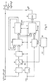
- the disturbed useful signal (e a (t)) is fed to both a low-pass filter (1) and a differential amplifier (9).
- the low-pass filter (1) is followed by an A / D converter (2) via a switch (10) which can be actuated by a controller (20), the outputs of which lead to inputs of a digital adder (4).
- the outputs of the digital adder (4) are connected both to the inputs of a shift register (6) and to the inputs of a computing unit (7).
- the outputs of the shift register (6) lead to further inputs of the adder (4).
- the outputs of the computing unit (7) lead via a D / A converter (8) to a negative input of the differential amplifier (9), at whose positive input the disturbed useful signal (e a (t)) is present.
- An n-fold frequency is generated from the causing interference signal (f a (t)) in a frequency multiplier (3).
- a period counter (5) counts the periods of the causing interference signal (f (t)) and passes the result on to the arithmetic unit (7).
- the A / D converter (2), the digital adder (4), the shift register (6) and the arithmetic unit (7) are clocked with the clock (T) generated by the frequency multiplier (3).
- the controller (20) is started at the start of a run by the power switch (22) and emits a start signal to the period counter (5), as well as an enable signal to the arithmetic unit (7) and a reset signal to the shift register (6) .
- this middle sample group - consisting of n average signal samples - provides a period of the frequency and phase in the disturbed useful signal (e a (t)) with the causing interference signal (f a (t) ) coupled signal parts, ie in particular the stationary additive hum components.
- an analog compensation signal (k a (t)) is generated from periodic phase locked with the causing interfering signal (f a (t) coupled repetition of the middle sample group. This repetition can be done, for example, by further circulation of the sample values accumulated in the shift register (6). Subtracting this compensation signal (k a (t)) from the disturbed useful signal (e a (t)) results in the desired interference-free or interference-reduced output signal (a a (t)).
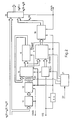
- FIG. 2 shows the basic circuit diagram of a circuit for digital input and output signals which operates on the same principle. All signals are indexed accordingly with "d".
- a digital low-pass filter (11) and a sampling rate converter (12) are used for a digitally disturbed useful signal (e d (t)), which converts the sampling rate from a digital signal of a compact disc of 44.1 kHz to n times the frequency of the interfering signal (f (t)).
- the switch (10) from Fig. 1 is replaced by switch (27).
- the number of switches (27) corresponds to the bit length of a sample.
- the conversion then takes place in a sampling rate converter (18).
- the determined correction value (k d (t)) is subtracted from the digitally disturbed useful signal (e d (t)) in a subtaker (19).
- the other circuit parts correspond to those in FIG. 1.
- a frequency- and phase-selective filter is implemented with simple digital means, the selection frequency of which, among other things. is determined by the causing interference signal (f (t)).
Landscapes
- Engineering & Computer Science (AREA)
- Physics & Mathematics (AREA)
- Computer Hardware Design (AREA)
- Mathematical Physics (AREA)
- Computer Networks & Wireless Communication (AREA)
- Signal Processing (AREA)
- Noise Elimination (AREA)
- Stabilization Of Oscillater, Synchronisation, Frequency Synthesizers (AREA)
- Analogue/Digital Conversion (AREA)
- Amplifiers (AREA)
Claims (9)
- Procédé pour la compensation numérique d'un signal parasite déterminé (n(t)) qui se forme en raison d'une interférence électrique ou magnétique dûe à un signal parasite qui cause la perturbation (f(t)) et qui intervient en superposition additive avec un signal utile (s(t)) dans un signal utile perturbé (e(t)), caractérisé en ce qu'un groupe de n valeurs de balayage est respectivement pris sur le signal utile perturbé dans au total m périodes (m étant un nombre entier) du signal qui cause la perturbation (f(t)) et au rythme (T) d'une n-ième fréquence (n étant un nombre entier) produite en étant couplée en phase avec le signal parasite qui cause la perturbation (f(t)), qu'à partir de ces m groupes de valeurs de balayage avec respectivement n valeurs de balayage un groupe moyen de balayage avec n valeurs de balayage est déterminé par moyenne arithmétique des valeurs de balayage prises respectivement en même relation de phase par rapport au signal parasite qui cause la perturbation (f(t)), que ce groupe moyen de valeurs de balayage est répété périodiquement dans la relation de phase d'origine en étant couplé en phase avec le signal parasite qui cause la perturbation (f(t)) et qu'un signal de compensation ainsi formé (k(t)) est soustrait en continu du signal utile perturbé (e(t)).
- Procédé selon la revendication 1, caractérisé en ce que le rythme (T) est obtenu à partir de la tension du réseau local d'alimentation en énergie par multiplication de la fréquence couplée en phase lorsqu'une composante de ronflement induite par le réseau doit être éliminée.
- Procédé selon la revendication 1, caractérisé en ce que le signal utile perturbé (e(t)) passe par un filtre passe-bas (1) analogique ou numérique avant le balayage, que la fréquence limite du passe-bas est choisie de telle manière qu'il n'est pas produit de pseudo-perturbations par le balayage subséquent et que des rotations de phase des composantes spectrales du signal parasite (n(t)) sont évitées ou compensées par le filtrage.
- Procédé selon la revendication 1, caractérisé en ce que le nombre de périodes m des m groupes de valeurs de balayage utilisés pour le calcul de la moyenne est une puissance de 2.
- Procédé selon la revendication 1, caractérisé en ce que les m groupes de valeurs de balayage sont déterminés à partir du signal utile perturbé (e(t)) pendant m périodes contiguës du signal parasite qui cause la perturbation (f(t)).
- Procédé selon la revendication 1, caractérisé en ce que les m groupes de valeurs de balayage sont déterminés à partir du signal utile perturbé (e(t)) pendant m périodes non contiguëes dans le temps du signal parasite qui cause la perturbation (f(t)).
- Procédé selon l'une ou plusieurs des revendications précédentes, caractérisé en ce que l'écart dans le temps entre respectivement deux des m périodes de balayage est un multiple entier fixe de la durée de période du signal parasite qui cause la perturbation (f(t)).
- Procédé selon l'une ou plusieurs des revendications précédentes, caractérisé en ce que l'écart dans le temps entre respectivement deux des m périodes de balayage est un multiple entier de la durée de période du signal parasite qui cause la perturbation (f(t)) qui est déterminé par un générateur de nombres aléatoires.
- Procédé selon l'une ou plusieurs des revendications précédentes, caractérisé en ce que le signal utile perturbé (e(t)) est balayé dans une formation de moyenne à échelle mobile pendant respectivement m périodes du signal parasite qui cause la perturbation (f(t)) et qu'il en est fait la moyenne et que le résultat de chaque dernière moyenne est utilisé comme signal de compensation (k(t)) pendant chaque période individuelle du signal parasite qui cause la perturbation (f(t)) par section.
Priority Applications (1)
| Application Number | Priority Date | Filing Date | Title |
|---|---|---|---|
| AT87103156T ATE85169T1 (de) | 1986-03-11 | 1987-03-05 | Schaltung zur digitalen kompensation eines determinierten stoersignals. |
Applications Claiming Priority (2)
| Application Number | Priority Date | Filing Date | Title |
|---|---|---|---|
| DE19863607928 DE3607928A1 (de) | 1986-03-11 | 1986-03-11 | Schaltung zur digitalen kompensation eines determinierten stoersignals |
| DE3607928 | 1986-03-11 |
Publications (3)
| Publication Number | Publication Date |
|---|---|
| EP0236956A2 EP0236956A2 (fr) | 1987-09-16 |
| EP0236956A3 EP0236956A3 (en) | 1989-03-29 |
| EP0236956B1 true EP0236956B1 (fr) | 1993-01-27 |
Family
ID=6295977
Family Applications (1)
| Application Number | Title | Priority Date | Filing Date |
|---|---|---|---|
| EP87103156A Expired - Lifetime EP0236956B1 (fr) | 1986-03-11 | 1987-03-05 | Circuit pour la compensation numérique d'un signal perturbateur déterminé |
Country Status (7)
| Country | Link |
|---|---|
| EP (1) | EP0236956B1 (fr) |
| JP (1) | JPS62284536A (fr) |
| KR (1) | KR920001546B1 (fr) |
| AT (1) | ATE85169T1 (fr) |
| DE (2) | DE3607928A1 (fr) |
| ES (1) | ES2038132T3 (fr) |
| HK (1) | HK120094A (fr) |
Families Citing this family (3)
| Publication number | Priority date | Publication date | Assignee | Title |
|---|---|---|---|---|
| AU662617B2 (en) * | 1992-04-06 | 1995-09-07 | Alcatel Australia Limited | A tone filter |
| US6151373A (en) * | 1997-04-03 | 2000-11-21 | At&T Corp. | Weak signal resolver |
| KR100635569B1 (ko) | 2004-09-23 | 2006-10-17 | 삼성에스디아이 주식회사 | 레이저 조사 장치 및 그를 이용한 유기 전계 발광 소자의제조 방법 |
Family Cites Families (5)
| Publication number | Priority date | Publication date | Assignee | Title |
|---|---|---|---|---|
| US4251831A (en) * | 1979-10-26 | 1981-02-17 | Kamath Bantval Y | Filter and system incorporating the filter for processing discrete samples of composite signals |
| JPS56104547A (en) * | 1980-01-25 | 1981-08-20 | Ntn Toyo Bearing Co Ltd | Noise eliminating circuit |
| JPS58107735A (ja) * | 1981-12-21 | 1983-06-27 | Matsushita Electric Ind Co Ltd | デ−タ送受信装置 |
| JPS6077556A (ja) * | 1983-10-05 | 1985-05-02 | Fujitsu Ltd | 干渉波除去法 |
| JPS6116028A (ja) * | 1984-06-30 | 1986-01-24 | Hitachi Maxell Ltd | 磁気記録媒体およびその製造方法 |
-
1986
- 1986-03-11 DE DE19863607928 patent/DE3607928A1/de not_active Withdrawn
-
1987
- 1987-03-05 ES ES198787103156T patent/ES2038132T3/es not_active Expired - Lifetime
- 1987-03-05 EP EP87103156A patent/EP0236956B1/fr not_active Expired - Lifetime
- 1987-03-05 AT AT87103156T patent/ATE85169T1/de not_active IP Right Cessation
- 1987-03-05 DE DE8787103156T patent/DE3783786D1/de not_active Expired - Fee Related
- 1987-03-11 JP JP62054281A patent/JPS62284536A/ja active Granted
- 1987-03-11 KR KR1019870002133A patent/KR920001546B1/ko not_active IP Right Cessation
-
1994
- 1994-11-03 HK HK120094A patent/HK120094A/xx not_active IP Right Cessation
Also Published As
| Publication number | Publication date |
|---|---|
| ATE85169T1 (de) | 1993-02-15 |
| JPS62284536A (ja) | 1987-12-10 |
| KR920001546B1 (ko) | 1992-02-18 |
| DE3607928A1 (de) | 1987-09-17 |
| HK120094A (en) | 1994-11-11 |
| KR880012038A (ko) | 1988-10-31 |
| ES2038132T3 (es) | 1993-07-16 |
| EP0236956A3 (en) | 1989-03-29 |
| JPH0519336B2 (fr) | 1993-03-16 |
| DE3783786D1 (de) | 1993-03-11 |
| EP0236956A2 (fr) | 1987-09-16 |
Similar Documents
| Publication | Publication Date | Title |
|---|---|---|
| DE60023526T2 (de) | Direkte digitale frequenzsynthese die störeliminierung ermöglicht | |
| DE10235062B4 (de) | Filterverfahren und A/D-Wandlergerät mit einer Filterfunktion | |
| DE4039122C2 (de) | Verfahren für einen Bildprozessor sowie Bildsignal-Kantenkorrekturschaltung zur Erzeugung eines kantenkorrigierten Bildsignals | |
| DE102015116269B4 (de) | Abtastratenwandler, analog-digital-wandler mit einem abtastratenwandler und verfahren zum umwandeln eines datenstroms von einer datenrate in eine andere datenrate | |
| EP0177076B1 (fr) | Circuit de conversion d'un signal de télévision analogique en signaux de couleurs numériques | |
| DE102005022586A1 (de) | Digitalauslöserfilter für ein Echtzeitdigitaloszilloskop | |
| DE4203879A1 (de) | Verfahren zur umwandlung eines messsignals und eines referenzsignals in ein ausgangssignal, sowie konverter zur durchfuehrung des verfahrens | |
| DE102006051364B4 (de) | Messverstärkungsvorrichtung und -verfahren | |
| DE102008023535A1 (de) | Elektronische Vorrichtung und Verfahren zur Auswertung einer variablen Kapazität | |
| DE4205352C2 (de) | Vorrichtung und Verfahren zum Gewinnen von Impulssignalen | |
| DE2831059C2 (de) | Integrierender Kodeumsetzer | |
| DE19524387C1 (de) | Schaltungsanordnung und Verfahren zum Messen eines Kapazitätsunterschiedes zwischen einer ersten Kapazität C1 und einer zweiten Kapazität C2 | |
| EP0236956B1 (fr) | Circuit pour la compensation numérique d'un signal perturbateur déterminé | |
| DE3533467C2 (de) | Verfahren und Anordnung zum störsicheren Erkennen von in Datensignalen enthaltenen Daten | |
| DE19510655B4 (de) | Schaltungsanordnung zum Filtern eines Stroms quantisierter elektrischer Signale und Verfahren zum Filtern eines Stoms quantisierter elektrischer Signale | |
| DE3836504C2 (fr) | ||
| DE3841388A1 (de) | Digitale fm-demodulatorvorrichtung | |
| DE2538544A1 (de) | Vorrichtung zur korrektur der abschattung von videobildern | |
| DE3621446A1 (de) | Geraet zum digitalen verarbeiten von kontinuierlichen bitstroemen | |
| DE102018129062B3 (de) | Filterverfahren und filter | |
| DE19944054B4 (de) | Anordnung zum Analysieren der nichtlinearen Eigenschaften eines Kommunikationskanals | |
| DE2607304C3 (de) | Schaltungsanordnung zum Erzeugen von Analogsignalen mit veränderbarer Folgefrequenz | |
| WO2001003295A1 (fr) | Filtre de decimation fir | |
| DE602005004818T2 (de) | Anordnung zum verstärken eines pwm-eingangssignals | |
| EP0676887B1 (fr) | Méthode à générer un signal sinus digital avec une fréquence d'échantillonnage prédéterminée et circuit pour la mise en oeuvre de la méthode |
Legal Events
| Date | Code | Title | Description |
|---|---|---|---|
| PUAI | Public reference made under article 153(3) epc to a published international application that has entered the european phase |
Free format text: ORIGINAL CODE: 0009012 |
|
| AK | Designated contracting states |
Kind code of ref document: A2 Designated state(s): AT BE CH DE ES FR GB GR IT LI LU NL SE |
|
| PUAL | Search report despatched |
Free format text: ORIGINAL CODE: 0009013 |
|
| AK | Designated contracting states |
Kind code of ref document: A3 Designated state(s): AT BE CH DE ES FR GB GR IT LI LU NL SE |
|
| 17P | Request for examination filed |
Effective date: 19890905 |
|
| 17Q | First examination report despatched |
Effective date: 19911017 |
|
| GRAA | (expected) grant |
Free format text: ORIGINAL CODE: 0009210 |
|
| AK | Designated contracting states |
Kind code of ref document: B1 Designated state(s): AT BE CH DE ES FR GB GR IT LI LU NL SE |
|
| PG25 | Lapsed in a contracting state [announced via postgrant information from national office to epo] |
Ref country code: GR Free format text: LAPSE BECAUSE OF FAILURE TO SUBMIT A TRANSLATION OF THE DESCRIPTION OR TO PAY THE FEE WITHIN THE PRESCRIBED TIME-LIMIT Effective date: 19930127 Ref country code: BE Effective date: 19930127 |
|
| REF | Corresponds to: |
Ref document number: 85169 Country of ref document: AT Date of ref document: 19930215 Kind code of ref document: T |
|
| ITF | It: translation for a ep patent filed |
Owner name: BARZANO' E ZANARDO MILANO S.P.A. |
|
| GBT | Gb: translation of ep patent filed (gb section 77(6)(a)/1977) |
Effective date: 19930122 |
|
| PG25 | Lapsed in a contracting state [announced via postgrant information from national office to epo] |
Ref country code: AT Effective date: 19930305 |
|
| REF | Corresponds to: |
Ref document number: 3783786 Country of ref document: DE Date of ref document: 19930311 |
|
| PG25 | Lapsed in a contracting state [announced via postgrant information from national office to epo] |
Ref country code: LU Free format text: LAPSE BECAUSE OF NON-PAYMENT OF DUE FEES Effective date: 19930331 Ref country code: LI Effective date: 19930331 Ref country code: CH Effective date: 19930331 |
|
| ET | Fr: translation filed | ||
| REG | Reference to a national code |
Ref country code: ES Ref legal event code: FG2A Ref document number: 2038132 Country of ref document: ES Kind code of ref document: T3 |
|
| PLBE | No opposition filed within time limit |
Free format text: ORIGINAL CODE: 0009261 |
|
| STAA | Information on the status of an ep patent application or granted ep patent |
Free format text: STATUS: NO OPPOSITION FILED WITHIN TIME LIMIT |
|
| REG | Reference to a national code |
Ref country code: CH Ref legal event code: PL |
|
| 26N | No opposition filed | ||
| EAL | Se: european patent in force in sweden |
Ref document number: 87103156.3 |
|
| REG | Reference to a national code |
Ref country code: GB Ref legal event code: 746 Effective date: 19970822 |
|
| REG | Reference to a national code |
Ref country code: FR Ref legal event code: D6 |
|
| REG | Reference to a national code |
Ref country code: GB Ref legal event code: IF02 |
|
| PGFP | Annual fee paid to national office [announced via postgrant information from national office to epo] |
Ref country code: FR Payment date: 20020315 Year of fee payment: 16 |
|
| PGFP | Annual fee paid to national office [announced via postgrant information from national office to epo] |
Ref country code: DE Payment date: 20020422 Year of fee payment: 16 |
|
| PGFP | Annual fee paid to national office [announced via postgrant information from national office to epo] |
Ref country code: GB Payment date: 20030210 Year of fee payment: 17 |
|
| PGFP | Annual fee paid to national office [announced via postgrant information from national office to epo] |
Ref country code: ES Payment date: 20030312 Year of fee payment: 17 |
|
| PGFP | Annual fee paid to national office [announced via postgrant information from national office to epo] |
Ref country code: SE Payment date: 20030324 Year of fee payment: 17 |
|
| PGFP | Annual fee paid to national office [announced via postgrant information from national office to epo] |
Ref country code: NL Payment date: 20030325 Year of fee payment: 17 |
|
| PG25 | Lapsed in a contracting state [announced via postgrant information from national office to epo] |
Ref country code: DE Free format text: LAPSE BECAUSE OF NON-PAYMENT OF DUE FEES Effective date: 20031001 |
|
| PG25 | Lapsed in a contracting state [announced via postgrant information from national office to epo] |
Ref country code: FR Free format text: LAPSE BECAUSE OF NON-PAYMENT OF DUE FEES Effective date: 20031127 |
|
| REG | Reference to a national code |
Ref country code: FR Ref legal event code: ST |
|
| PG25 | Lapsed in a contracting state [announced via postgrant information from national office to epo] |
Ref country code: GB Free format text: LAPSE BECAUSE OF NON-PAYMENT OF DUE FEES Effective date: 20040305 |
|
| PG25 | Lapsed in a contracting state [announced via postgrant information from national office to epo] |
Ref country code: SE Free format text: LAPSE BECAUSE OF NON-PAYMENT OF DUE FEES Effective date: 20040306 Ref country code: ES Free format text: LAPSE BECAUSE OF NON-PAYMENT OF DUE FEES Effective date: 20040306 |
|
| PG25 | Lapsed in a contracting state [announced via postgrant information from national office to epo] |
Ref country code: NL Free format text: LAPSE BECAUSE OF NON-PAYMENT OF DUE FEES Effective date: 20041001 |
|
| GBPC | Gb: european patent ceased through non-payment of renewal fee | ||
| EUG | Se: european patent has lapsed | ||
| NLV4 | Nl: lapsed or anulled due to non-payment of the annual fee |
Effective date: 20041001 |
|
| PG25 | Lapsed in a contracting state [announced via postgrant information from national office to epo] |
Ref country code: IT Free format text: LAPSE BECAUSE OF NON-PAYMENT OF DUE FEES;WARNING: LAPSES OF ITALIAN PATENTS WITH EFFECTIVE DATE BEFORE 2007 MAY HAVE OCCURRED AT ANY TIME BEFORE 2007. THE CORRECT EFFECTIVE DATE MAY BE DIFFERENT FROM THE ONE RECORDED. Effective date: 20050305 |
|
| REG | Reference to a national code |
Ref country code: ES Ref legal event code: FD2A Effective date: 20040306 |