EP0223469A2 - Light receiving members - Google Patents
Light receiving members Download PDFInfo
- Publication number
- EP0223469A2 EP0223469A2 EP86308521A EP86308521A EP0223469A2 EP 0223469 A2 EP0223469 A2 EP 0223469A2 EP 86308521 A EP86308521 A EP 86308521A EP 86308521 A EP86308521 A EP 86308521A EP 0223469 A2 EP0223469 A2 EP 0223469A2
- Authority
- EP
- European Patent Office
- Prior art keywords
- layer
- atoms
- light receiving
- receiving member
- support
- Prior art date
- Legal status (The legal status is an assumption and is not a legal conclusion. Google has not performed a legal analysis and makes no representation as to the accuracy of the status listed.)
- Granted
Links
- 239000010410 layer Substances 0.000 claims abstract description 396
- 239000002344 surface layer Substances 0.000 claims abstract description 69
- GNPVGFCGXDBREM-UHFFFAOYSA-N germanium atom Chemical group [Ge] GNPVGFCGXDBREM-UHFFFAOYSA-N 0.000 claims abstract description 54
- ATJFFYVFTNAWJD-UHFFFAOYSA-N Tin Chemical group [Sn] ATJFFYVFTNAWJD-UHFFFAOYSA-N 0.000 claims abstract description 35
- 239000000463 material Substances 0.000 claims abstract description 27
- 238000005299 abrasion Methods 0.000 claims abstract description 20
- 230000003449 preventive effect Effects 0.000 claims abstract description 20
- XUIMIQQOPSSXEZ-UHFFFAOYSA-N Silicon Chemical group [Si] XUIMIQQOPSSXEZ-UHFFFAOYSA-N 0.000 claims abstract description 17
- 239000000470 constituent Substances 0.000 claims description 50
- 125000004432 carbon atom Chemical group C* 0.000 claims description 46
- 125000004430 oxygen atom Chemical group O* 0.000 claims description 44
- 125000004433 nitrogen atom Chemical group N* 0.000 claims description 43
- 239000000126 substance Substances 0.000 claims description 18
- 230000005764 inhibitory process Effects 0.000 claims description 11
- 238000002347 injection Methods 0.000 claims description 10
- 239000007924 injection Substances 0.000 claims description 10
- 230000004888 barrier function Effects 0.000 claims description 6
- 229910001506 inorganic fluoride Inorganic materials 0.000 claims description 5
- 229910052809 inorganic oxide Inorganic materials 0.000 claims description 5
- 229910052751 metal Inorganic materials 0.000 claims description 5
- 239000002184 metal Substances 0.000 claims description 5
- 229910052945 inorganic sulfide Inorganic materials 0.000 claims description 4
- 229910021417 amorphous silicon Inorganic materials 0.000 abstract description 46
- 230000001427 coherent effect Effects 0.000 abstract description 5
- 125000004429 atom Chemical group 0.000 description 120
- 239000007789 gas Substances 0.000 description 102
- 238000000034 method Methods 0.000 description 79
- 239000007858 starting material Substances 0.000 description 78
- 230000008569 process Effects 0.000 description 51
- 238000009826 distribution Methods 0.000 description 47
- 238000004544 sputter deposition Methods 0.000 description 42
- 125000004435 hydrogen atom Chemical group [H]* 0.000 description 41
- 229910052799 carbon Inorganic materials 0.000 description 34
- 125000005843 halogen group Chemical group 0.000 description 33
- 229910052757 nitrogen Inorganic materials 0.000 description 33
- 229910052710 silicon Inorganic materials 0.000 description 31
- 230000007423 decrease Effects 0.000 description 30
- 239000010703 silicon Substances 0.000 description 26
- -1 NiCr Chemical class 0.000 description 25
- 238000000151 deposition Methods 0.000 description 25
- 238000007599 discharging Methods 0.000 description 25
- 230000008021 deposition Effects 0.000 description 24
- 230000000694 effects Effects 0.000 description 15
- 239000000203 mixture Substances 0.000 description 15
- 238000004519 manufacturing process Methods 0.000 description 14
- 230000001276 controlling effect Effects 0.000 description 13
- IJGRMHOSHXDMSA-UHFFFAOYSA-N Atomic nitrogen Chemical compound N#N IJGRMHOSHXDMSA-UHFFFAOYSA-N 0.000 description 12
- 239000012298 atmosphere Substances 0.000 description 12
- LZDSILRDTDCIQT-UHFFFAOYSA-N dinitrogen trioxide Chemical compound [O-][N+](=O)N=O LZDSILRDTDCIQT-UHFFFAOYSA-N 0.000 description 12
- 210000002381 plasma Anatomy 0.000 description 12
- BLRPTPMANUNPDV-UHFFFAOYSA-N Silane Chemical class [SiH4] BLRPTPMANUNPDV-UHFFFAOYSA-N 0.000 description 10
- VYPSYNLAJGMNEJ-UHFFFAOYSA-N Silicium dioxide Chemical compound O=[Si]=O VYPSYNLAJGMNEJ-UHFFFAOYSA-N 0.000 description 10
- MCMNRKCIXSYSNV-UHFFFAOYSA-N Zirconium dioxide Chemical compound O=[Zr]=O MCMNRKCIXSYSNV-UHFFFAOYSA-N 0.000 description 10
- 230000015572 biosynthetic process Effects 0.000 description 10
- 229910052732 germanium Inorganic materials 0.000 description 10
- VNWKTOKETHGBQD-UHFFFAOYSA-N methane Chemical compound C VNWKTOKETHGBQD-UHFFFAOYSA-N 0.000 description 10
- 238000006243 chemical reaction Methods 0.000 description 9
- 230000003287 optical effect Effects 0.000 description 9
- 239000004065 semiconductor Substances 0.000 description 9
- QGZKDVFQNNGYKY-UHFFFAOYSA-N Ammonia Chemical compound N QGZKDVFQNNGYKY-UHFFFAOYSA-N 0.000 description 8
- GWEVSGVZZGPLCZ-UHFFFAOYSA-N Titan oxide Chemical compound O=[Ti]=O GWEVSGVZZGPLCZ-UHFFFAOYSA-N 0.000 description 8
- 229910052782 aluminium Inorganic materials 0.000 description 8
- WFPZPJSADLPSON-UHFFFAOYSA-N dinitrogen tetraoxide Chemical compound [O-][N+](=O)[N+]([O-])=O WFPZPJSADLPSON-UHFFFAOYSA-N 0.000 description 8
- 229910052739 hydrogen Inorganic materials 0.000 description 8
- 229910010272 inorganic material Inorganic materials 0.000 description 8
- 238000007733 ion plating Methods 0.000 description 8
- 229910052718 tin Inorganic materials 0.000 description 8
- 206010034972 Photosensitivity reaction Diseases 0.000 description 7
- 229910004014 SiF4 Inorganic materials 0.000 description 7
- 229910000577 Silicon-germanium Inorganic materials 0.000 description 7
- 229910021627 Tin(IV) chloride Inorganic materials 0.000 description 7
- 238000010790 dilution Methods 0.000 description 7
- 239000012895 dilution Substances 0.000 description 7
- 238000010438 heat treatment Methods 0.000 description 7
- 230000036961 partial effect Effects 0.000 description 7
- 230000036211 photosensitivity Effects 0.000 description 7
- ABTOQLMXBSRXSM-UHFFFAOYSA-N silicon tetrafluoride Chemical compound F[Si](F)(F)F ABTOQLMXBSRXSM-UHFFFAOYSA-N 0.000 description 7
- 239000000758 substrate Substances 0.000 description 7
- HPGGPRDJHPYFRM-UHFFFAOYSA-J tin(iv) chloride Chemical compound Cl[Sn](Cl)(Cl)Cl HPGGPRDJHPYFRM-UHFFFAOYSA-J 0.000 description 7
- 229910006160 GeF4 Inorganic materials 0.000 description 6
- OAKJQQAXSVQMHS-UHFFFAOYSA-N Hydrazine Chemical compound NN OAKJQQAXSVQMHS-UHFFFAOYSA-N 0.000 description 6
- VEXZGXHMUGYJMC-UHFFFAOYSA-N Hydrochloric acid Chemical compound Cl VEXZGXHMUGYJMC-UHFFFAOYSA-N 0.000 description 6
- ATUOYWHBWRKTHZ-UHFFFAOYSA-N Propane Chemical compound CCC ATUOYWHBWRKTHZ-UHFFFAOYSA-N 0.000 description 6
- HSFWRNGVRCDJHI-UHFFFAOYSA-N alpha-acetylene Natural products C#C HSFWRNGVRCDJHI-UHFFFAOYSA-N 0.000 description 6
- 229910052786 argon Inorganic materials 0.000 description 6
- 230000003247 decreasing effect Effects 0.000 description 6
- ZWWCURLKEXEFQT-UHFFFAOYSA-N dinitrogen pentaoxide Chemical compound [O-][N+](=O)O[N+]([O-])=O ZWWCURLKEXEFQT-UHFFFAOYSA-N 0.000 description 6
- 229910052736 halogen Inorganic materials 0.000 description 6
- 150000002367 halogens Chemical class 0.000 description 6
- 229930195733 hydrocarbon Natural products 0.000 description 6
- 150000002430 hydrocarbons Chemical class 0.000 description 6
- 238000002156 mixing Methods 0.000 description 6
- 230000002829 reductive effect Effects 0.000 description 6
- 238000007788 roughening Methods 0.000 description 6
- PPMWWXLUCOODDK-UHFFFAOYSA-N tetrafluorogermane Chemical compound F[Ge](F)(F)F PPMWWXLUCOODDK-UHFFFAOYSA-N 0.000 description 6
- GQPLMRYTRLFLPF-UHFFFAOYSA-N Nitrous Oxide Chemical compound [O-][N+]#N GQPLMRYTRLFLPF-UHFFFAOYSA-N 0.000 description 5
- 229910007264 Si2H6 Inorganic materials 0.000 description 5
- 229910052581 Si3N4 Inorganic materials 0.000 description 5
- XAGFODPZIPBFFR-UHFFFAOYSA-N aluminium Chemical compound [Al] XAGFODPZIPBFFR-UHFFFAOYSA-N 0.000 description 5
- 238000000149 argon plasma sintering Methods 0.000 description 5
- 229910052681 coesite Inorganic materials 0.000 description 5
- 229910052906 cristobalite Inorganic materials 0.000 description 5
- 238000005520 cutting process Methods 0.000 description 5
- PZPGRFITIJYNEJ-UHFFFAOYSA-N disilane Chemical compound [SiH3][SiH3] PZPGRFITIJYNEJ-UHFFFAOYSA-N 0.000 description 5
- 239000011261 inert gas Substances 0.000 description 5
- 150000002484 inorganic compounds Chemical class 0.000 description 5
- 239000007788 liquid Substances 0.000 description 5
- 150000004756 silanes Chemical class 0.000 description 5
- 239000000377 silicon dioxide Substances 0.000 description 5
- 235000012239 silicon dioxide Nutrition 0.000 description 5
- 229910052682 stishovite Inorganic materials 0.000 description 5
- 229910052905 tridymite Inorganic materials 0.000 description 5
- MGWGWNFMUOTEHG-UHFFFAOYSA-N 4-(3,5-dimethylphenyl)-1,3-thiazol-2-amine Chemical compound CC1=CC(C)=CC(C=2N=C(N)SC=2)=C1 MGWGWNFMUOTEHG-UHFFFAOYSA-N 0.000 description 4
- 229910000838 Al alloy Inorganic materials 0.000 description 4
- XKRFYHLGVUSROY-UHFFFAOYSA-N Argon Chemical compound [Ar] XKRFYHLGVUSROY-UHFFFAOYSA-N 0.000 description 4
- ZOXJGFHDIHLPTG-UHFFFAOYSA-N Boron Chemical group [B] ZOXJGFHDIHLPTG-UHFFFAOYSA-N 0.000 description 4
- VGGSQFUCUMXWEO-UHFFFAOYSA-N Ethene Chemical compound C=C VGGSQFUCUMXWEO-UHFFFAOYSA-N 0.000 description 4
- MWUXSHHQAYIFBG-UHFFFAOYSA-N Nitric oxide Chemical compound O=[N] MWUXSHHQAYIFBG-UHFFFAOYSA-N 0.000 description 4
- OFBQJSOFQDEBGM-UHFFFAOYSA-N Pentane Chemical compound CCCCC OFBQJSOFQDEBGM-UHFFFAOYSA-N 0.000 description 4
- PNEYBMLMFCGWSK-UHFFFAOYSA-N aluminium oxide Inorganic materials [O-2].[O-2].[O-2].[Al+3].[Al+3] PNEYBMLMFCGWSK-UHFFFAOYSA-N 0.000 description 4
- 229910052593 corundum Inorganic materials 0.000 description 4
- 239000013078 crystal Substances 0.000 description 4
- 239000010408 film Substances 0.000 description 4
- 229910052986 germanium hydride Inorganic materials 0.000 description 4
- 239000001257 hydrogen Substances 0.000 description 4
- JUINSXZKUKVTMD-UHFFFAOYSA-N hydrogen azide Chemical compound N=[N+]=[N-] JUINSXZKUKVTMD-UHFFFAOYSA-N 0.000 description 4
- IJDNQMDRQITEOD-UHFFFAOYSA-N n-butane Chemical compound CCCC IJDNQMDRQITEOD-UHFFFAOYSA-N 0.000 description 4
- JCXJVPUVTGWSNB-UHFFFAOYSA-N nitrogen dioxide Inorganic materials O=[N]=O JCXJVPUVTGWSNB-UHFFFAOYSA-N 0.000 description 4
- 229910052698 phosphorus Inorganic materials 0.000 description 4
- 125000004805 propylene group Chemical group [H]C([H])([H])C([H])([*:1])C([H])([H])[*:2] 0.000 description 4
- 229920005989 resin Polymers 0.000 description 4
- 239000011347 resin Substances 0.000 description 4
- 229910001220 stainless steel Inorganic materials 0.000 description 4
- 238000012360 testing method Methods 0.000 description 4
- XOLBLPGZBRYERU-UHFFFAOYSA-N tin dioxide Chemical compound O=[Sn]=O XOLBLPGZBRYERU-UHFFFAOYSA-N 0.000 description 4
- 238000012546 transfer Methods 0.000 description 4
- 238000009827 uniform distribution Methods 0.000 description 4
- 238000005406 washing Methods 0.000 description 4
- 229910001845 yogo sapphire Inorganic materials 0.000 description 4
- OKTJSMMVPCPJKN-UHFFFAOYSA-N Carbon Chemical compound [C] OKTJSMMVPCPJKN-UHFFFAOYSA-N 0.000 description 3
- PXGOKWXKJXAPGV-UHFFFAOYSA-N Fluorine Chemical compound FF PXGOKWXKJXAPGV-UHFFFAOYSA-N 0.000 description 3
- UFHFLCQGNIYNRP-UHFFFAOYSA-N Hydrogen Chemical compound [H][H] UFHFLCQGNIYNRP-UHFFFAOYSA-N 0.000 description 3
- 229910005096 Si3H8 Inorganic materials 0.000 description 3
- HEMHJVSKTPXQMS-UHFFFAOYSA-M Sodium hydroxide Chemical compound [OH-].[Na+] HEMHJVSKTPXQMS-UHFFFAOYSA-M 0.000 description 3
- 239000002253 acid Substances 0.000 description 3
- 239000007864 aqueous solution Substances 0.000 description 3
- QVGXLLKOCUKJST-UHFFFAOYSA-N atomic oxygen Chemical compound [O] QVGXLLKOCUKJST-UHFFFAOYSA-N 0.000 description 3
- 229910052796 boron Inorganic materials 0.000 description 3
- 229910052804 chromium Inorganic materials 0.000 description 3
- VNNRSPGTAMTISX-UHFFFAOYSA-N chromium nickel Chemical compound [Cr].[Ni] VNNRSPGTAMTISX-UHFFFAOYSA-N 0.000 description 3
- 230000002950 deficient Effects 0.000 description 3
- 239000012777 electrically insulating material Substances 0.000 description 3
- 238000005530 etching Methods 0.000 description 3
- 229910052731 fluorine Inorganic materials 0.000 description 3
- 239000011737 fluorine Substances 0.000 description 3
- QUZPNFFHZPRKJD-UHFFFAOYSA-N germane Chemical compound [GeH4] QUZPNFFHZPRKJD-UHFFFAOYSA-N 0.000 description 3
- 150000004820 halides Chemical class 0.000 description 3
- 150000002366 halogen compounds Chemical class 0.000 description 3
- 239000011147 inorganic material Substances 0.000 description 3
- 230000001788 irregular Effects 0.000 description 3
- 229910001120 nichrome Inorganic materials 0.000 description 3
- PXHVJJICTQNCMI-UHFFFAOYSA-N nickel Substances [Ni] PXHVJJICTQNCMI-UHFFFAOYSA-N 0.000 description 3
- 229910052758 niobium Inorganic materials 0.000 description 3
- 229910052760 oxygen Inorganic materials 0.000 description 3
- 239000001301 oxygen Substances 0.000 description 3
- 229910052697 platinum Inorganic materials 0.000 description 3
- 229910021420 polycrystalline silicon Inorganic materials 0.000 description 3
- 230000035945 sensitivity Effects 0.000 description 3
- 150000003377 silicon compounds Chemical class 0.000 description 3
- 239000002356 single layer Substances 0.000 description 3
- 229910052715 tantalum Inorganic materials 0.000 description 3
- 238000001771 vacuum deposition Methods 0.000 description 3
- 229910052720 vanadium Inorganic materials 0.000 description 3
- 230000004304 visual acuity Effects 0.000 description 3
- KLZUFWVZNOTSEM-UHFFFAOYSA-K Aluminium flouride Chemical compound F[Al](F)F KLZUFWVZNOTSEM-UHFFFAOYSA-K 0.000 description 2
- MJBPUQUGJNAPAZ-UHFFFAOYSA-N Butine Natural products O1C2=CC(O)=CC=C2C(=O)CC1C1=CC=C(O)C(O)=C1 MJBPUQUGJNAPAZ-UHFFFAOYSA-N 0.000 description 2
- ZAMOUSCENKQFHK-UHFFFAOYSA-N Chlorine atom Chemical compound [Cl] ZAMOUSCENKQFHK-UHFFFAOYSA-N 0.000 description 2
- OTMSDBZUPAUEDD-UHFFFAOYSA-N Ethane Chemical compound CC OTMSDBZUPAUEDD-UHFFFAOYSA-N 0.000 description 2
- 239000005977 Ethylene Substances 0.000 description 2
- KRHYYFGTRYWZRS-UHFFFAOYSA-N Fluorane Chemical compound F KRHYYFGTRYWZRS-UHFFFAOYSA-N 0.000 description 2
- VQTUBCCKSQIDNK-UHFFFAOYSA-N Isobutene Chemical group CC(C)=C VQTUBCCKSQIDNK-UHFFFAOYSA-N 0.000 description 2
- CBENFWSGALASAD-UHFFFAOYSA-N Ozone Chemical compound [O-][O+]=O CBENFWSGALASAD-UHFFFAOYSA-N 0.000 description 2
- XYFCBTPGUUZFHI-UHFFFAOYSA-N Phosphine Chemical class P XYFCBTPGUUZFHI-UHFFFAOYSA-N 0.000 description 2
- 229910003816 SiH2F2 Inorganic materials 0.000 description 2
- 229910003822 SiHCl3 Inorganic materials 0.000 description 2
- 229910000831 Steel Inorganic materials 0.000 description 2
- QAOWNCQODCNURD-UHFFFAOYSA-N Sulfuric acid Chemical compound OS(O)(=O)=O QAOWNCQODCNURD-UHFFFAOYSA-N 0.000 description 2
- 238000010521 absorption reaction Methods 0.000 description 2
- 239000003513 alkali Substances 0.000 description 2
- VSCWAEJMTAWNJL-UHFFFAOYSA-K aluminium trichloride Chemical compound Cl[Al](Cl)Cl VSCWAEJMTAWNJL-UHFFFAOYSA-K 0.000 description 2
- 229910021529 ammonia Inorganic materials 0.000 description 2
- 229910052787 antimony Inorganic materials 0.000 description 2
- UAZDIGCOBKKMPU-UHFFFAOYSA-O azanium;azide Chemical compound [NH4+].[N-]=[N+]=[N-] UAZDIGCOBKKMPU-UHFFFAOYSA-O 0.000 description 2
- ILAHWRKJUDSMFH-UHFFFAOYSA-N boron tribromide Chemical compound BrB(Br)Br ILAHWRKJUDSMFH-UHFFFAOYSA-N 0.000 description 2
- 230000005587 bubbling Effects 0.000 description 2
- IAQRGUVFOMOMEM-UHFFFAOYSA-N butene Natural products CC=CC IAQRGUVFOMOMEM-UHFFFAOYSA-N 0.000 description 2
- 230000015556 catabolic process Effects 0.000 description 2
- 239000000919 ceramic Substances 0.000 description 2
- 238000005229 chemical vapour deposition Methods 0.000 description 2
- 239000000460 chlorine Substances 0.000 description 2
- 229910052801 chlorine Inorganic materials 0.000 description 2
- 238000004140 cleaning Methods 0.000 description 2
- 239000011248 coating agent Substances 0.000 description 2
- 238000000576 coating method Methods 0.000 description 2
- 239000010730 cutting oil Substances 0.000 description 2
- 238000013461 design Methods 0.000 description 2
- 238000011161 development Methods 0.000 description 2
- 229910003460 diamond Inorganic materials 0.000 description 2
- 239000010432 diamond Substances 0.000 description 2
- KBDJQNUZLNUGDS-UHFFFAOYSA-N dibromosilicon Chemical compound Br[Si]Br KBDJQNUZLNUGDS-UHFFFAOYSA-N 0.000 description 2
- MGNHOGAVECORPT-UHFFFAOYSA-N difluorosilicon Chemical compound F[Si]F MGNHOGAVECORPT-UHFFFAOYSA-N 0.000 description 2
- RNRZLEZABHZRSX-UHFFFAOYSA-N diiodosilicon Chemical compound I[Si]I RNRZLEZABHZRSX-UHFFFAOYSA-N 0.000 description 2
- KPUWHANPEXNPJT-UHFFFAOYSA-N disiloxane Chemical compound [SiH3]O[SiH3] KPUWHANPEXNPJT-UHFFFAOYSA-N 0.000 description 2
- 238000010894 electron beam technology Methods 0.000 description 2
- 125000002534 ethynyl group Chemical group [H]C#C* 0.000 description 2
- 230000003631 expected effect Effects 0.000 description 2
- 238000002474 experimental method Methods 0.000 description 2
- 229910052733 gallium Inorganic materials 0.000 description 2
- AHVNUGPIPKMDBB-UHFFFAOYSA-N germanium Chemical compound [Ge].[Ge].[Ge] AHVNUGPIPKMDBB-UHFFFAOYSA-N 0.000 description 2
- VGRFVJMYCCLWPQ-UHFFFAOYSA-N germanium Chemical compound [Ge].[Ge] VGRFVJMYCCLWPQ-UHFFFAOYSA-N 0.000 description 2
- YBMRDBCBODYGJE-UHFFFAOYSA-N germanium dioxide Chemical compound O=[Ge]=O YBMRDBCBODYGJE-UHFFFAOYSA-N 0.000 description 2
- 239000011521 glass Substances 0.000 description 2
- 238000000227 grinding Methods 0.000 description 2
- 230000006872 improvement Effects 0.000 description 2
- PJXISJQVUVHSOJ-UHFFFAOYSA-N indium(III) oxide Inorganic materials [O-2].[O-2].[O-2].[In+3].[In+3] PJXISJQVUVHSOJ-UHFFFAOYSA-N 0.000 description 2
- PSCMQHVBLHHWTO-UHFFFAOYSA-K indium(iii) chloride Chemical compound Cl[In](Cl)Cl PSCMQHVBLHHWTO-UHFFFAOYSA-K 0.000 description 2
- 238000009434 installation Methods 0.000 description 2
- 229910052741 iridium Inorganic materials 0.000 description 2
- 229910001635 magnesium fluoride Inorganic materials 0.000 description 2
- 150000002739 metals Chemical class 0.000 description 2
- QKCGXXHCELUCKW-UHFFFAOYSA-N n-[4-[4-(dinaphthalen-2-ylamino)phenyl]phenyl]-n-naphthalen-2-ylnaphthalen-2-amine Chemical compound C1=CC=CC2=CC(N(C=3C=CC(=CC=3)C=3C=CC(=CC=3)N(C=3C=C4C=CC=CC4=CC=3)C=3C=C4C=CC=CC4=CC=3)C3=CC4=CC=CC=C4C=C3)=CC=C21 QKCGXXHCELUCKW-UHFFFAOYSA-N 0.000 description 2
- 229910052759 nickel Inorganic materials 0.000 description 2
- 229910000069 nitrogen hydride Inorganic materials 0.000 description 2
- 229960001730 nitrous oxide Drugs 0.000 description 2
- YWAKXRMUMFPDSH-UHFFFAOYSA-N pentene Chemical compound CCCC=C YWAKXRMUMFPDSH-UHFFFAOYSA-N 0.000 description 2
- 230000000737 periodic effect Effects 0.000 description 2
- 239000011574 phosphorus Substances 0.000 description 2
- 239000000049 pigment Substances 0.000 description 2
- 239000004033 plastic Substances 0.000 description 2
- 229920003023 plastic Polymers 0.000 description 2
- 238000005498 polishing Methods 0.000 description 2
- 229920000515 polycarbonate Polymers 0.000 description 2
- 239000004417 polycarbonate Substances 0.000 description 2
- 238000012545 processing Methods 0.000 description 2
- 239000001294 propane Substances 0.000 description 2
- QQONPFPTGQHPMA-UHFFFAOYSA-N propylene Natural products CC=C QQONPFPTGQHPMA-UHFFFAOYSA-N 0.000 description 2
- MWWATHDPGQKSAR-UHFFFAOYSA-N propyne Chemical group CC#C MWWATHDPGQKSAR-UHFFFAOYSA-N 0.000 description 2
- 238000005546 reactive sputtering Methods 0.000 description 2
- 238000005488 sandblasting Methods 0.000 description 2
- 229930195734 saturated hydrocarbon Natural products 0.000 description 2
- 239000007787 solid Substances 0.000 description 2
- KXCAEQNNTZANTK-UHFFFAOYSA-N stannane Chemical compound [SnH4] KXCAEQNNTZANTK-UHFFFAOYSA-N 0.000 description 2
- 239000010959 steel Substances 0.000 description 2
- 230000003746 surface roughness Effects 0.000 description 2
- 229920003002 synthetic resin Polymers 0.000 description 2
- 239000000057 synthetic resin Substances 0.000 description 2
- 229910052716 thallium Inorganic materials 0.000 description 2
- 239000010409 thin film Substances 0.000 description 2
- 229910000083 tin tetrahydride Inorganic materials 0.000 description 2
- ZSUXOVNWDZTCFN-UHFFFAOYSA-L tin(ii) bromide Chemical compound Br[Sn]Br ZSUXOVNWDZTCFN-UHFFFAOYSA-L 0.000 description 2
- JTDNNCYXCFHBGG-UHFFFAOYSA-L tin(ii) iodide Chemical compound I[Sn]I JTDNNCYXCFHBGG-UHFFFAOYSA-L 0.000 description 2
- QPBYLOWPSRZOFX-UHFFFAOYSA-J tin(iv) iodide Chemical compound I[Sn](I)(I)I QPBYLOWPSRZOFX-UHFFFAOYSA-J 0.000 description 2
- 229910052719 titanium Inorganic materials 0.000 description 2
- IAQRGUVFOMOMEM-ONEGZZNKSA-N trans-but-2-ene Chemical compound C\C=C\C IAQRGUVFOMOMEM-ONEGZZNKSA-N 0.000 description 2
- ZQTYRTSKQFQYPQ-UHFFFAOYSA-N trisiloxane Chemical compound [SiH3]O[SiH2]O[SiH3] ZQTYRTSKQFQYPQ-UHFFFAOYSA-N 0.000 description 2
- 238000007740 vapor deposition Methods 0.000 description 2
- UOCLXMDMGBRAIB-UHFFFAOYSA-N 1,1,1-trichloroethane Chemical compound CC(Cl)(Cl)Cl UOCLXMDMGBRAIB-UHFFFAOYSA-N 0.000 description 1
- ZCYVEMRRCGMTRW-UHFFFAOYSA-N 7553-56-2 Chemical compound [I] ZCYVEMRRCGMTRW-UHFFFAOYSA-N 0.000 description 1
- 229910021630 Antimony pentafluoride Inorganic materials 0.000 description 1
- 229910017011 AsBr3 Inorganic materials 0.000 description 1
- 229910017009 AsCl3 Inorganic materials 0.000 description 1
- 229910017050 AsF3 Inorganic materials 0.000 description 1
- 229910017049 AsF5 Inorganic materials 0.000 description 1
- 229910015845 BBr3 Inorganic materials 0.000 description 1
- 229910015844 BCl3 Inorganic materials 0.000 description 1
- 229910015898 BF4 Inorganic materials 0.000 description 1
- 229910014263 BrF3 Inorganic materials 0.000 description 1
- 229910001369 Brass Inorganic materials 0.000 description 1
- WKBOTKDWSSQWDR-UHFFFAOYSA-N Bromine atom Chemical compound [Br] WKBOTKDWSSQWDR-UHFFFAOYSA-N 0.000 description 1
- 229910020187 CeF3 Inorganic materials 0.000 description 1
- 229910020323 ClF3 Inorganic materials 0.000 description 1
- 101100441092 Danio rerio crlf3 gene Proteins 0.000 description 1
- GYHNNYVSQQEPJS-UHFFFAOYSA-N Gallium Chemical compound [Ga] GYHNNYVSQQEPJS-UHFFFAOYSA-N 0.000 description 1
- 229910006109 GeBr4 Inorganic materials 0.000 description 1
- 229910006111 GeCl2 Inorganic materials 0.000 description 1
- 229910006113 GeCl4 Inorganic materials 0.000 description 1
- 229910006158 GeF2 Inorganic materials 0.000 description 1
- 229910006162 GeI2 Inorganic materials 0.000 description 1
- 229910006149 GeI4 Inorganic materials 0.000 description 1
- 229910021600 Germanium(II) bromide Inorganic materials 0.000 description 1
- 229910020667 PBr3 Inorganic materials 0.000 description 1
- 229910020656 PBr5 Inorganic materials 0.000 description 1
- OAICVXFJPJFONN-UHFFFAOYSA-N Phosphorus Chemical compound [P] OAICVXFJPJFONN-UHFFFAOYSA-N 0.000 description 1
- 239000004952 Polyamide Substances 0.000 description 1
- 239000004698 Polyethylene Substances 0.000 description 1
- 239000004743 Polypropylene Substances 0.000 description 1
- 239000004793 Polystyrene Substances 0.000 description 1
- 229920001328 Polyvinylidene chloride Polymers 0.000 description 1
- 229910007159 Si(CH3)4 Inorganic materials 0.000 description 1
- 229910003676 SiBr4 Inorganic materials 0.000 description 1
- 229910003910 SiCl4 Inorganic materials 0.000 description 1
- 229910003818 SiH2Cl2 Inorganic materials 0.000 description 1
- 229910020328 SiSn Inorganic materials 0.000 description 1
- 229910021626 Tin(II) chloride Inorganic materials 0.000 description 1
- 229910021623 Tin(IV) bromide Inorganic materials 0.000 description 1
- XSTXAVWGXDQKEL-UHFFFAOYSA-N Trichloroethylene Chemical group ClC=C(Cl)Cl XSTXAVWGXDQKEL-UHFFFAOYSA-N 0.000 description 1
- SYKNUAWMBRIEKB-UHFFFAOYSA-N [Cl].[Br] Chemical compound [Cl].[Br] SYKNUAWMBRIEKB-UHFFFAOYSA-N 0.000 description 1
- 229910017875 a-SiN Inorganic materials 0.000 description 1
- 238000000862 absorption spectrum Methods 0.000 description 1
- 230000009471 action Effects 0.000 description 1
- 125000000217 alkyl group Chemical group 0.000 description 1
- 229910045601 alloy Inorganic materials 0.000 description 1
- 239000000956 alloy Substances 0.000 description 1
- WATWJIUSRGPENY-UHFFFAOYSA-N antimony atom Chemical compound [Sb] WATWJIUSRGPENY-UHFFFAOYSA-N 0.000 description 1
- 229910000074 antimony hydride Inorganic materials 0.000 description 1
- VBVBHWZYQGJZLR-UHFFFAOYSA-I antimony pentafluoride Chemical compound F[Sb](F)(F)(F)F VBVBHWZYQGJZLR-UHFFFAOYSA-I 0.000 description 1
- FAPDDOBMIUGHIN-UHFFFAOYSA-K antimony trichloride Chemical compound Cl[Sb](Cl)Cl FAPDDOBMIUGHIN-UHFFFAOYSA-K 0.000 description 1
- GUNJVIDCYZYFGV-UHFFFAOYSA-K antimony trifluoride Chemical compound F[Sb](F)F GUNJVIDCYZYFGV-UHFFFAOYSA-K 0.000 description 1
- VMPVEPPRYRXYNP-UHFFFAOYSA-I antimony(5+);pentachloride Chemical compound Cl[Sb](Cl)(Cl)(Cl)Cl VMPVEPPRYRXYNP-UHFFFAOYSA-I 0.000 description 1
- RBFQJDQYXXHULB-UHFFFAOYSA-N arsane Chemical compound [AsH3] RBFQJDQYXXHULB-UHFFFAOYSA-N 0.000 description 1
- 229910052785 arsenic Inorganic materials 0.000 description 1
- RQNWIZPPADIBDY-UHFFFAOYSA-N arsenic atom Chemical compound [As] RQNWIZPPADIBDY-UHFFFAOYSA-N 0.000 description 1
- 229910000070 arsenic hydride Inorganic materials 0.000 description 1
- YBGKQGSCGDNZIB-UHFFFAOYSA-N arsenic pentafluoride Chemical compound F[As](F)(F)(F)F YBGKQGSCGDNZIB-UHFFFAOYSA-N 0.000 description 1
- JMBNQWNFNACVCB-UHFFFAOYSA-N arsenic tribromide Chemical compound Br[As](Br)Br JMBNQWNFNACVCB-UHFFFAOYSA-N 0.000 description 1
- OEYOHULQRFXULB-UHFFFAOYSA-N arsenic trichloride Chemical compound Cl[As](Cl)Cl OEYOHULQRFXULB-UHFFFAOYSA-N 0.000 description 1
- JCMGUODNZMETBM-UHFFFAOYSA-N arsenic trifluoride Chemical compound F[As](F)F JCMGUODNZMETBM-UHFFFAOYSA-N 0.000 description 1
- 230000005540 biological transmission Effects 0.000 description 1
- 229910052797 bismuth Inorganic materials 0.000 description 1
- JCXGWMGPZLAOME-UHFFFAOYSA-N bismuth atom Chemical compound [Bi] JCXGWMGPZLAOME-UHFFFAOYSA-N 0.000 description 1
- JHXKRIRFYBPWGE-UHFFFAOYSA-K bismuth chloride Chemical compound Cl[Bi](Cl)Cl JHXKRIRFYBPWGE-UHFFFAOYSA-K 0.000 description 1
- 229910000072 bismuth hydride Inorganic materials 0.000 description 1
- TXKAQZRUJUNDHI-UHFFFAOYSA-K bismuth tribromide Chemical compound Br[Bi](Br)Br TXKAQZRUJUNDHI-UHFFFAOYSA-K 0.000 description 1
- BPBOBPIKWGUSQG-UHFFFAOYSA-N bismuthane Chemical compound [BiH3] BPBOBPIKWGUSQG-UHFFFAOYSA-N 0.000 description 1
- 238000007664 blowing Methods 0.000 description 1
- UORVGPXVDQYIDP-UHFFFAOYSA-N borane Chemical class B UORVGPXVDQYIDP-UHFFFAOYSA-N 0.000 description 1
- 239000010951 brass Substances 0.000 description 1
- GDTBXPJZTBHREO-UHFFFAOYSA-N bromine Substances BrBr GDTBXPJZTBHREO-UHFFFAOYSA-N 0.000 description 1
- 229910052794 bromium Inorganic materials 0.000 description 1
- 229920002301 cellulose acetate Polymers 0.000 description 1
- CETPSERCERDGAM-UHFFFAOYSA-N ceric oxide Chemical compound O=[Ce]=O CETPSERCERDGAM-UHFFFAOYSA-N 0.000 description 1
- 229910000422 cerium(IV) oxide Inorganic materials 0.000 description 1
- 239000003795 chemical substances by application Substances 0.000 description 1
- KRVSOGSZCMJSLX-UHFFFAOYSA-L chromic acid Substances O[Cr](O)(=O)=O KRVSOGSZCMJSLX-UHFFFAOYSA-L 0.000 description 1
- 150000001875 compounds Chemical class 0.000 description 1
- 238000007796 conventional method Methods 0.000 description 1
- 230000007547 defect Effects 0.000 description 1
- 238000007872 degassing Methods 0.000 description 1
- 238000006731 degradation reaction Methods 0.000 description 1
- 230000006866 deterioration Effects 0.000 description 1
- DUVPPTXIBVUIKL-UHFFFAOYSA-N dibromogermanium Chemical compound Br[Ge]Br DUVPPTXIBVUIKL-UHFFFAOYSA-N 0.000 description 1
- IAGYEMVJHPEPGE-UHFFFAOYSA-N diiodogermanium Chemical compound I[Ge]I IAGYEMVJHPEPGE-UHFFFAOYSA-N 0.000 description 1
- 239000003085 diluting agent Substances 0.000 description 1
- 229910001873 dinitrogen Inorganic materials 0.000 description 1
- 239000012153 distilled water Substances 0.000 description 1
- 230000005611 electricity Effects 0.000 description 1
- 238000004049 embossing Methods 0.000 description 1
- 238000004534 enameling Methods 0.000 description 1
- 230000008020 evaporation Effects 0.000 description 1
- 238000001704 evaporation Methods 0.000 description 1
- AWJWCTOOIBYHON-UHFFFAOYSA-N furo[3,4-b]pyrazine-5,7-dione Chemical compound C1=CN=C2C(=O)OC(=O)C2=N1 AWJWCTOOIBYHON-UHFFFAOYSA-N 0.000 description 1
- QHGIKMVOLGCZIP-UHFFFAOYSA-N germanium dichloride Chemical compound Cl[Ge]Cl QHGIKMVOLGCZIP-UHFFFAOYSA-N 0.000 description 1
- GGJOARIBACGTDV-UHFFFAOYSA-N germanium difluoride Chemical compound F[Ge]F GGJOARIBACGTDV-UHFFFAOYSA-N 0.000 description 1
- 229910052737 gold Inorganic materials 0.000 description 1
- 229910002804 graphite Inorganic materials 0.000 description 1
- 239000010439 graphite Substances 0.000 description 1
- 150000002431 hydrogen Chemical class 0.000 description 1
- 229910000039 hydrogen halide Inorganic materials 0.000 description 1
- 239000012433 hydrogen halide Substances 0.000 description 1
- 239000012535 impurity Substances 0.000 description 1
- 229910052738 indium Inorganic materials 0.000 description 1
- APFVFJFRJDLVQX-UHFFFAOYSA-N indium atom Chemical compound [In] APFVFJFRJDLVQX-UHFFFAOYSA-N 0.000 description 1
- PNDPGZBMCMUPRI-UHFFFAOYSA-N iodine Chemical compound II PNDPGZBMCMUPRI-UHFFFAOYSA-N 0.000 description 1
- 229910052740 iodine Inorganic materials 0.000 description 1
- 239000011630 iodine Substances 0.000 description 1
- 230000001678 irradiating effect Effects 0.000 description 1
- 238000010030 laminating Methods 0.000 description 1
- 238000003475 lamination Methods 0.000 description 1
- 229910052745 lead Inorganic materials 0.000 description 1
- 230000004298 light response Effects 0.000 description 1
- 238000003801 milling Methods 0.000 description 1
- 229910052750 molybdenum Inorganic materials 0.000 description 1
- 229910021421 monocrystalline silicon Inorganic materials 0.000 description 1
- 150000004767 nitrides Chemical class 0.000 description 1
- 229910017464 nitrogen compound Inorganic materials 0.000 description 1
- 150000002830 nitrogen compounds Chemical class 0.000 description 1
- 239000001272 nitrous oxide Substances 0.000 description 1
- 239000000346 nonvolatile oil Substances 0.000 description 1
- 230000003647 oxidation Effects 0.000 description 1
- 238000007254 oxidation reaction Methods 0.000 description 1
- 238000010422 painting Methods 0.000 description 1
- 229910052763 palladium Inorganic materials 0.000 description 1
- 239000000123 paper Substances 0.000 description 1
- 125000004437 phosphorous atom Chemical group 0.000 description 1
- UHZYTMXLRWXGPK-UHFFFAOYSA-N phosphorus pentachloride Chemical compound ClP(Cl)(Cl)(Cl)Cl UHZYTMXLRWXGPK-UHFFFAOYSA-N 0.000 description 1
- OBCUTHMOOONNBS-UHFFFAOYSA-N phosphorus pentafluoride Chemical compound FP(F)(F)(F)F OBCUTHMOOONNBS-UHFFFAOYSA-N 0.000 description 1
- IPNPIHIZVLFAFP-UHFFFAOYSA-N phosphorus tribromide Chemical compound BrP(Br)Br IPNPIHIZVLFAFP-UHFFFAOYSA-N 0.000 description 1
- FAIAAWCVCHQXDN-UHFFFAOYSA-N phosphorus trichloride Chemical compound ClP(Cl)Cl FAIAAWCVCHQXDN-UHFFFAOYSA-N 0.000 description 1
- WKFBZNUBXWCCHG-UHFFFAOYSA-N phosphorus trifluoride Chemical compound FP(F)F WKFBZNUBXWCCHG-UHFFFAOYSA-N 0.000 description 1
- 229920002647 polyamide Polymers 0.000 description 1
- 229920000728 polyester Polymers 0.000 description 1
- 229920006267 polyester film Polymers 0.000 description 1
- 229920000573 polyethylene Polymers 0.000 description 1
- 229920001155 polypropylene Polymers 0.000 description 1
- 229920002223 polystyrene Polymers 0.000 description 1
- 229920000915 polyvinyl chloride Polymers 0.000 description 1
- 239000004800 polyvinyl chloride Substances 0.000 description 1
- 239000005033 polyvinylidene chloride Substances 0.000 description 1
- 238000002360 preparation method Methods 0.000 description 1
- 230000009467 reduction Effects 0.000 description 1
- 230000001105 regulatory effect Effects 0.000 description 1
- 230000004044 response Effects 0.000 description 1
- 229920006395 saturated elastomer Polymers 0.000 description 1
- 229910052990 silicon hydride Inorganic materials 0.000 description 1
- AIFMYMZGQVTROK-UHFFFAOYSA-N silicon tetrabromide Chemical compound Br[Si](Br)(Br)Br AIFMYMZGQVTROK-UHFFFAOYSA-N 0.000 description 1
- FDNAPBUWERUEDA-UHFFFAOYSA-N silicon tetrachloride Chemical compound Cl[Si](Cl)(Cl)Cl FDNAPBUWERUEDA-UHFFFAOYSA-N 0.000 description 1
- 229910052709 silver Inorganic materials 0.000 description 1
- PUZPDOWCWNUUKD-UHFFFAOYSA-M sodium fluoride Inorganic materials [F-].[Na+] PUZPDOWCWNUUKD-UHFFFAOYSA-M 0.000 description 1
- 235000011121 sodium hydroxide Nutrition 0.000 description 1
- 239000002904 solvent Substances 0.000 description 1
- 229910052950 sphalerite Inorganic materials 0.000 description 1
- 235000011150 stannous chloride Nutrition 0.000 description 1
- ANOBYBYXJXCGBS-UHFFFAOYSA-L stannous fluoride Chemical compound F[Sn]F ANOBYBYXJXCGBS-UHFFFAOYSA-L 0.000 description 1
- 230000003068 static effect Effects 0.000 description 1
- OUULRIDHGPHMNQ-UHFFFAOYSA-N stibane Chemical compound [SbH3] OUULRIDHGPHMNQ-UHFFFAOYSA-N 0.000 description 1
- 238000004381 surface treatment Methods 0.000 description 1
- PBCFLUZVCVVTBY-UHFFFAOYSA-N tantalum pentoxide Inorganic materials O=[Ta](=O)O[Ta](=O)=O PBCFLUZVCVVTBY-UHFFFAOYSA-N 0.000 description 1
- 238000005496 tempering Methods 0.000 description 1
- VJHDVMPJLLGYBL-UHFFFAOYSA-N tetrabromogermane Chemical compound Br[Ge](Br)(Br)Br VJHDVMPJLLGYBL-UHFFFAOYSA-N 0.000 description 1
- IEXRMSFAVATTJX-UHFFFAOYSA-N tetrachlorogermane Chemical compound Cl[Ge](Cl)(Cl)Cl IEXRMSFAVATTJX-UHFFFAOYSA-N 0.000 description 1
- CUDGTZJYMWAJFV-UHFFFAOYSA-N tetraiodogermane Chemical compound I[Ge](I)(I)I CUDGTZJYMWAJFV-UHFFFAOYSA-N 0.000 description 1
- CZDYPVPMEAXLPK-UHFFFAOYSA-N tetramethylsilane Chemical compound C[Si](C)(C)C CZDYPVPMEAXLPK-UHFFFAOYSA-N 0.000 description 1
- BKVIYDNLLOSFOA-UHFFFAOYSA-N thallium Chemical compound [Tl] BKVIYDNLLOSFOA-UHFFFAOYSA-N 0.000 description 1
- KTZHUTMWYRHVJB-UHFFFAOYSA-K thallium(3+);trichloride Chemical compound Cl[Tl](Cl)Cl KTZHUTMWYRHVJB-UHFFFAOYSA-K 0.000 description 1
- 150000003568 thioethers Chemical class 0.000 description 1
- AXZWODMDQAVCJE-UHFFFAOYSA-L tin(II) chloride (anhydrous) Chemical compound [Cl-].[Cl-].[Sn+2] AXZWODMDQAVCJE-UHFFFAOYSA-L 0.000 description 1
- LTSUHJWLSNQKIP-UHFFFAOYSA-J tin(iv) bromide Chemical compound Br[Sn](Br)(Br)Br LTSUHJWLSNQKIP-UHFFFAOYSA-J 0.000 description 1
- FAQYAMRNWDIXMY-UHFFFAOYSA-N trichloroborane Chemical compound ClB(Cl)Cl FAQYAMRNWDIXMY-UHFFFAOYSA-N 0.000 description 1
- UBOXGVDOUJQMTN-UHFFFAOYSA-N trichloroethylene Natural products ClCC(Cl)Cl UBOXGVDOUJQMTN-UHFFFAOYSA-N 0.000 description 1
- FQFKTKUFHWNTBN-UHFFFAOYSA-N trifluoro-$l^{3}-bromane Chemical compound FBr(F)F FQFKTKUFHWNTBN-UHFFFAOYSA-N 0.000 description 1
- JOHWNGGYGAVMGU-UHFFFAOYSA-N trifluorochlorine Chemical compound FCl(F)F JOHWNGGYGAVMGU-UHFFFAOYSA-N 0.000 description 1
- XLYOFNOQVPJJNP-UHFFFAOYSA-N water Chemical compound O XLYOFNOQVPJJNP-UHFFFAOYSA-N 0.000 description 1
- 229910052725 zinc Inorganic materials 0.000 description 1
- 229910052984 zinc sulfide Inorganic materials 0.000 description 1
Images


Classifications
-
- G—PHYSICS
- G03—PHOTOGRAPHY; CINEMATOGRAPHY; ANALOGOUS TECHNIQUES USING WAVES OTHER THAN OPTICAL WAVES; ELECTROGRAPHY; HOLOGRAPHY
- G03G—ELECTROGRAPHY; ELECTROPHOTOGRAPHY; MAGNETOGRAPHY
- G03G5/00—Recording members for original recording by exposure, e.g. to light, to heat, to electrons; Manufacture thereof; Selection of materials therefor
- G03G5/02—Charge-receiving layers
- G03G5/04—Photoconductive layers; Charge-generation layers or charge-transporting layers; Additives therefor; Binders therefor
- G03G5/08—Photoconductive layers; Charge-generation layers or charge-transporting layers; Additives therefor; Binders therefor characterised by the photoconductive material being inorganic
- G03G5/082—Photoconductive layers; Charge-generation layers or charge-transporting layers; Additives therefor; Binders therefor characterised by the photoconductive material being inorganic and not being incorporated in a bonding material, e.g. vacuum deposited
- G03G5/08214—Silicon-based
- G03G5/08235—Silicon-based comprising three or four silicon-based layers
- G03G5/08242—Silicon-based comprising three or four silicon-based layers at least one with varying composition
-
- G—PHYSICS
- G03—PHOTOGRAPHY; CINEMATOGRAPHY; ANALOGOUS TECHNIQUES USING WAVES OTHER THAN OPTICAL WAVES; ELECTROGRAPHY; HOLOGRAPHY
- G03G—ELECTROGRAPHY; ELECTROPHOTOGRAPHY; MAGNETOGRAPHY
- G03G5/00—Recording members for original recording by exposure, e.g. to light, to heat, to electrons; Manufacture thereof; Selection of materials therefor
- G03G5/02—Charge-receiving layers
- G03G5/04—Photoconductive layers; Charge-generation layers or charge-transporting layers; Additives therefor; Binders therefor
- G03G5/08—Photoconductive layers; Charge-generation layers or charge-transporting layers; Additives therefor; Binders therefor characterised by the photoconductive material being inorganic
- G03G5/082—Photoconductive layers; Charge-generation layers or charge-transporting layers; Additives therefor; Binders therefor characterised by the photoconductive material being inorganic and not being incorporated in a bonding material, e.g. vacuum deposited
- G03G5/08214—Silicon-based
- G03G5/08235—Silicon-based comprising three or four silicon-based layers
-
- G—PHYSICS
- G03—PHOTOGRAPHY; CINEMATOGRAPHY; ANALOGOUS TECHNIQUES USING WAVES OTHER THAN OPTICAL WAVES; ELECTROGRAPHY; HOLOGRAPHY
- G03G—ELECTROGRAPHY; ELECTROPHOTOGRAPHY; MAGNETOGRAPHY
- G03G5/00—Recording members for original recording by exposure, e.g. to light, to heat, to electrons; Manufacture thereof; Selection of materials therefor
- G03G5/10—Bases for charge-receiving or other layers
-
- G—PHYSICS
- G03—PHOTOGRAPHY; CINEMATOGRAPHY; ANALOGOUS TECHNIQUES USING WAVES OTHER THAN OPTICAL WAVES; ELECTROGRAPHY; HOLOGRAPHY
- G03G—ELECTROGRAPHY; ELECTROPHOTOGRAPHY; MAGNETOGRAPHY
- G03G5/00—Recording members for original recording by exposure, e.g. to light, to heat, to electrons; Manufacture thereof; Selection of materials therefor
- G03G5/14—Inert intermediate or cover layers for charge-receiving layers
- G03G5/147—Cover layers
- G03G5/14704—Cover layers comprising inorganic material
Definitions
- This invention concerns light receiving members being sensitive to electromagnetic waves such as light (which herein means in a broader sense those lights such as ultra-violet rays, visible rays, infrared rays, X-rays, and Y-rays). More specifically, the invention relates to improved light receiving members suitable particularly for use in the case where coherent lights such as laser beams are applied.
- those light receiving members for electro-photography being suitable for use in the case of using the semiconductor laser
- those light receiving members comprising amorphous materials containing silicon atoms (hereinafter referred to as "a-Si"), for example, as disclosed in Japanese Patent Laid-Open Nos. 8634l/l979 and 83746/l98l, have been evaluated as being worthy of attention since they have a high Vickers hardness and cause less problems in the public pollution, in addition to their excellent matching property in the photosensitive region as compared with other kinds of known light receiving members.
- the light receiving layer constituting the light receiving member as described above is formed as an a-Si layer of mono-layer structure, it is necessary to structurally incorporate hydrogen or halogen atoms or, further, boron atoms within a range of specific amount into the layer in order to maintain the required dark resistance of greater than l012 ⁇ cm as for the electrophotography while maintaining their high photosensitivity. Therefore, the degree of freedom for the design of the light receiving member undergoes a rather severe limit such as the requirement for the strict control for various kinds of conditions upon forming the layer. Then, there have been made several proposals to overcome such problems for the degree of freedom in view of the design in that the high photosensitivity can effectively be utilized while reducing the dark resistance to some extent.
- the light receiving layer is so constituted as to have two or more layers prepared by laminating those layers for different conductivity in which a depletion layer is formed to the inside of the light receiving layer as disclosed in Japanese Patent Laid-Open Nos. l7l743/l979, 4053/l982, and 4l72/l982, or the apparent dark resistance is improved by providing a multi-layered structure in which a barrier layer is disposed between the support and the light receiving layer and/or on the upper surface of the light receiving layer as disclosed, for example, in Japanese Patent Laid-Open Nos. 52l78/l982, 52l79/l982, 52l80/l982, 58l59/l982, 58l60/l982, and 58l6l/l982.
- such light receiving members as having a light receiving layer of multi-layered structure have unevenness in the thickness for each of the layers.
- the laser beams comprise coherent monochromatic light
- the respective reflection lights reflected from the free surface of the light receiving layer on the side of the laser beam irradiation and from the layer boundary between each of the layers constituting the light receiving layer and between the support and the light receiving layer (hereinafter both of the free surface and the layer interface are collectively referred to as "interface") often interfere with each other.
- the interference results in a so-called interference fringe pattern in the formed images which brings about defective images. Particularly, in the case of intermediate tone images with high gradation, the images obtained become extremely poor in identification.
- interference effects occur as for each of the layers, and those interference effects are synergistically acted with each other to exhibit interference fringe patterns, which directly influence on the transfer member thereby to transfer and fix the interference fringe on the member, and thus bringing about defective images in the visible images corresponding to the interference fringe pattern.
- the method (c) referring to incident light for instance, a portion of the incident light is reflected at the surface of the light receiving layer to be a reflected light, while the remaining portion intrudes as the transmitted light to the inside of the light receiving layer. And a portion of the transmitted light is scattered as a diffused light at the surface of the support and the remaining portion is regularly reflected as a reflected light, a portion of which goes out as the outgoing light.
- the outgoing light is a component to interfere with the reflected light. In any way, since the light is remaining, the interference fringe pattern cannot be completely eliminated.
- the support surface is roughened irregularly, the reflected light at the surface of the first layer, the reflected light at the second layer, and the regular reflected light at the support surface interfere with one another to result in the interference fringe pattern in accordance with the thickness of each layer in the light receiving member. Accordingly, it is impossible to completely prevent the interference fringe by unevenly roughening the surface of the support in the light receiving member of the multi-layered structure.
- the inclined surface on the unevenness at the support are in parallel with the inclined surface on the unevenness at the light receiving layer, where the incident light brings about bright and dark areas. Further, in the light receiving layer, since the layer thickness is not uniform over the entire light receiving layer, dark and bright stripe pattern occurs. Accordingly, mere orderly roughening the surface of the support cannot completely prevent the occurrence of the interference fringe pattern.
- the situation is more complicated than the occurrence of the interference fringe in the light receiving member of single layer structure.
- the object of this invention is to provide a light receiving member comprising a light receiving layer mainly composed of a-Si, free from the foregoing problems and capable of satisfying various kinds of requirements.
- the main object of this invention is to provide a light receiving member comprising a light receiving layer constituted with a-Si in which electrical, pitical, and photoconductive properties are always substantially stable scarcely depending on the working circumstances, and which is excellent against optical fatigue, causes no degradation upon repeating use, excellent in durability and moisture-proofness, exhibits no or scarce residual potential and provides easy production control.
- Another object of this invention is to provide a light receiving member comprising a light receiving layer composed of a-Si which has a high photosensitivity in the entire visible region of light, particularly, an excellent matching property with a semiconductor laser, and shows quick light response.
- Another object of this invention is to provide a light receiving member comprising a light receiving layer composed of a-Si which has high photosensitivity, high S/N ratio, and high electrical voltage withstanding property.
- a further object of this invention is to provide a light receiving member comprising a light receiving layer composed of a-Si which is excellent in the close bondability between the support and the layer disposed on the support or between the laminated layers,strict and stable in that of the structural arrangement and of high layer quality.
- a further object of this invention is to provide a light receiving member comprising a light receiving layer composed of a-Si which is suitable to the image formation by using a-Si which is suitable to the image formation by using coherent light, free from the occurrence of interference fringe pattern and spot upon reversed development even after repeating use for a long period of time, free from defective images or blurring in the images, shows high density with clear half tone, and has a high resolving power, and can provide high quality images.
- the present inventors have made earnest studies for overcoming the foregoing problems on the conventional light receiving members and attaining the objects as described above and, as a result, have accomplished this invention based on the findings as described below.
- this invention relates to a light receiving member which is characterized by comprising a support and a light receiving layer having a photosensitive layer composed of amorphous material containing silicon atoms and at least either germanium atoms or tin atoms and a surface layer, said surface layer being of multi-layered structure having at least an abrasion-resistant layer at the outermost side and a reflection preventive layer in the inside, and said support having a surface provided with irregularities composed of spherical dimples each of which having an inside face provided with minute irregularities.
- one finding is that in a light receiving member equipped with a light receiving layer having a photosensitive layer and a surface layer on a support (substrate), when the surface layer is constituted as a multi-layered structure having an abrasion-resistant layer at the outermost side and at least a reflection preventive layer in the side, the reflection of the incident light at the interface between the surface layer and the photosensitive layer can be prevented, and the problems such as the interference fringe or uneven sensitivity resulted from the uneven layer thickness upon forming the surface layer and/or uneven layer thickness due to the abrasion of the surface layer can be overcome.
- Another finding is that the problems for the interference fringe pattern occurring upon image formation in the light receiving member having a plurality of layers on a support can be overcome by disposing unevenness constituted with a plurality of spherical dimples each of which having an inside face provided with minute irregularities on the surface of the support.
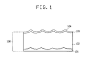
- Figure l is a schematic view illustrating the layer structure of the light receiving member l00 pertaining to this invention.
- the light receiving member is made up of the support l0l, a photosensitive layer l02 and a surface layer l03 respectively formed thereon.
- the support l0l has a support surface provided with irregularities composed of a plurality of fine spherical dimples each of which having an inside face provided with minute irregularities.
- the photosensitive layer l02 and th surface layer l03 are formed along the slopes of the irregularities.
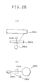
- Figures 2 and 3 are views explaining how the problem of interference infringe pattern is solved in the light receiving member of this invention.
- Figure 3 is an enlarged view for a portion of a conventional light receiving member in which a light receiving layer of a multi-layered structure is deposited on the support, the surface of which is regularly roughened.
- 30l is a photosensitive layer
- 302 is a surface layer
- 303 is a free surface
- 304 is an interface between the photosensitive layer and the surface layer.
- the light receiving layer is usually formed along the uneven shape at the surface of the support, the slope of the unevenness at the surface of the support and the slope of the unevenness of the light receiving layer are in parallel with each other.
- the following problems always occur, for example, in a light receiving member of multi-layered structure in which the light receiving layer comprises two layers, that is, the photosensitive layer 30l and the surface layer 302. Since the interface 304 between the photosensitive layer and the surface layer is in parallel with the free surface 303, the direction of the reflected light R1 at the interface 304 and that of the reflected light R2 at the free surface coincide with each other and, accordingly, an interference fringe occurs depending on the thickness of the surface layer.
- Figure 2 is an enlarged view for a portion shown in Figure l.
- an uneven shape composed of a plurality of fine spherical dimples each of which having an inside face provided with minute irregularities (not shown) are formed at the surface of the support in the light receiving member according to this invention and the light receiving layer thereover is deposited along the uneven shape. Therefore, in the light receiving member of the multi-layered structure, for example, in which the light receiving layer comprises a photosensitive layer 20l and a surface layer 202, the interface 204 between the photosensitive layer 20l and the surface layer 202 and the free surface 203 are respectively formed with the uneven shape composed of the spherical dimples along the uneven shape at the surface of the support.
- the deviation of the wavelength represented by l1 + l2 - l3 by using l1, l2, and l3 shown in Figure 2 is not constant but variable, by which a sharing interference corresponding to the so-called Newton ring phenomenon occurs and the interference fringe is dispersed within the dimples. Then, if the interference ring should appear in the microscopic point of view in the images caused by way of the light receiving member, it is not visually recognized.
- the fringe pattern resulted in the images due to the interference between lights passing through the light receiving layer and reflecting on the layer interface and at the surface of the support thereby enabling to obtain a light receiving member capable of forming excellent images.
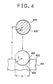
- Figure 4 is a schematic view for a typical example of the shape at the support surface in the light receiving member according to this invention shown in Figure l, in which a portion of the uneven shape is enlarged and are shown a support 40l and a support surface 402 composed of a spherical dimple 403 having an inside surface provided with minute irregularities 404, 404, ...
- desirable scattering effects are brought about due to the minute irregularities in addition to the interference preventive effect as above explained referring to Figure 2 thereby the occurrence of an interference fringe pattern being more certainly prevented, and the following problems,which are observed for the conventional light receiving members are effectively eliminated.
- the blade collides mainly against a convex part of the uneven surface shape of the light receiving layer to cause problems that cleaning is not perfected and not only an abrasion of the convex part of the light receiving layer but also that of the surface of the blade becomes greater thereby their durabilities being decreased.
- the radius of curvature R and the width D of the uneven shape formed by the spherical dimples, at the surface of the support of the light receiving member according to this invention constitute an important factor for effectively attaining the advantageous effects of preventing the occurrence of the interference fringe in the light receiving member according to this invention.
- the present inventors carried out various experiments and, as a result, found the following facts.
- the ratio D/R is greater than 0.035 and, preferably, greater than 0.055 for dispersing the interference fringes resulted throughout the light receiving member in each of the dimples thereby preventing the occurrence of the interference fringe in the light receiving member.
- the width D of the unevenness formed by the scraped dimple is about 500 ⁇ m at the maximum, preferably, less than 200 ⁇ m and, more preferably less than l00 ⁇ m.
- the height of a minute irregularity to be formed with the inside face of a spherical dimple of the support namely the surface roughness ⁇ max of the inside face of the spherical dimple lies in the range of 0.5 to 20 ⁇ m. That is, in the case where said ⁇ max is less than 0.5 ⁇ m, a sufficient scattering effect is not be given. And in the case where it exceeds 20 ⁇ m, the magnitude of the minute irregularity becomes undesirably greater in comparison with that of the spherical dimple to prevent the spherical dimple from being formed in a desired spherical form and result in bringing about such a light receiving member that does not prevent sufficiently the occurrence of the interference fringe.
- the light receiving member as prepared becomes to have such a light receiving layer that is accompanied by an undesirably grown unevenness being apt to invite defects in visible images to be formed.
- the light receiving layer of the light receiving member which is disposed on the.surface having the particular surface as above-mentioned in this invention is constituted by the photosensitive layer and the surface layer.
- the photosensitive layer is composed of amorphous materia containing silicon atoms and at least either germanium atoms or tin atoms, particularly preferably, of amorphous material containing silicon atoms(Si), at least either germanium atoms(Ge) or tin atoms(Sn), and at least either hydrogen atoms (H) or halogen atoms(X) [hereinafter referred to as "a-Si(Ge,Sn) (H,X)"] or of a-Si(Ge,Sn)(H,X) containing at least one kind selected from oxygen atoms(O), carbon atoms(C) and nitrogen atoms(N) [hereinafter referred to as "a-Si(Ge,Sn)(O,C,N)(H,X
- the photosensitive layer may be of a multi-layered structure and, particularly preferably it includes a charge injection inhibition layer containing a substance to control the conductivity as one of the constituent layers and/or a barrier layer as one of the constituent layers.
- the surface layer may be composed of amorphous mateiral containing silicon atoms, at least one kind selected from oxygen atoms(O), carbon atoms(C) and nitrogen atoms(N) and, preferably in addition to these, at least either hydrogen atoms(H) or halogen atoms(X) [hereinafter referred to as "a-Si(O,C,N)(H,X)"], or may be composed of at least one kind selected from inorganic fluorides, inorganic oxides and inorganic sulfides.
- the surface layer is multi-layered to have at least an abrasion-resistant layer at the outermost side and a refection preventive layer in the inside.
- vacuum deposition technique such as glow discharging method, sputtering method or ion plating method, but other than these methods, optical CVD method and heat CVD method may be also employed.
- the support l0l in the light receiving member according to this invention has a surface with fine unevenness smaller than the resolution power required for the light receiving member and the unevenness is composed of a plurality of spherical dimples each of which having an inside face provided with minute irregularities.
- Figure 4 is a schematic view for a typical example of the shape at the surface of the support in the light receiving member according to this invention, in which a portion of the uneven shape is enlarged.
- FIG 4 are shown a support 40l, a support surface 402, an irregular shape due to a spherical dimple (spherical cavity pit)403, an inside face of the spherical dimple provided with minute irregularities 404, and a rigid sphere 403′ of which surface has irregularities 404′.
- Figure 4 also shows an example of the preferred methods of preparing the surface shape of the support. That is, the rigid sphere 403′ is caused to fall gravitationally from a position at a predetermined height above the support surface 402 and collides against the support surface 402 thereby forming the spherical dimple having the inside face provided with minute irregularities 404. And a plurality of the spherical dimples 403 each substantially of an almost identical radius of curvature R and of an almost identical width D can be formed to the support surface 402 by causing a plurality of the rigid spheres 403′ substantially of an identical diameter of curvature R′ to fall from identical height h simultaneously or sequentially.
- Figures 5(A) through 5(C) show typical embodiments of supports formed with the uneven shape composed of a plurality of spherical dimples each of which having an inside surface provided with minute irregularities at the surface as described above.
- FIGS 5(A) through 5(C) are shown a support 50l, a support surface 502, a spherical dimple (spherical cavity pit) having an inside face provided with minute irregularities (not shown) 504 or 504′ and a rigid sphere of which surface has minute irregularities (not shown) 503 or 503′.
- a plurality of dimples (spherical cavity pits) 503, 503, ... of an almost identical radius of curvature and of an almost identical width are formed while being closely overlapped with each other thereby forming an uneven shape regularly by causing to fall a plurality of spheres 503′, 503′, ... regularly from an identical height to different positions at the support surface 502 of the support 50l.
- a plurality of dimples 504, 504′, ... having two kinds of diameter of curvature and two kinds of width are formed being densely overlapped with each other to the surface 502 of the support 50l thereby forming an unevenness with irregular height at the surface by dropping two kinds of spheres 503, 503′, ... of different diameters from the hieghts identical with or different from each other.
- a plurality of dimples 504, 504, ... of an almost identical diameter of curvature and plural kinds of width are formed while being overlapped with each other thereby forming an irregular unevenness by causing to fall a plurality of spheres 503, 503, ... of an identical diameter from the identical height irregularly to the surface 502 of the support 50l.
- the uneven shape of the support surface composed of the spherical dimples each of which having an inside face provided with irregularities can be formed preferably by dropping the rigid spheres respectively of a surface provided with minute irregularities to the support surface.
- a plurality of spherical dimples having desired radius of curvature and width can be formed at a predetermined density on the support surface by properly selecting various conditions such as the diameter of the rigid spheres, falling height, hardness for the rigid sphere and the support surface or the amount of the fallen spheres. That is, the height and the pitch of the uneven shape formed for the support surface can optionally be adjusted depending on the given purpose by selecting various conditions as described above thereby enabling to obtain a support having a desired uneven shape with the support surface.
- the support l0l for use in this invention may either be electroconductive or insulative.
- the electroconductive support can include, for example, metals such as NiCr, stainless steels, Al, Cr, Mo, Au, Nb, Ta, V, Ti, Pt and Pb or the alloys thereof.
- the electrically insulative support can include, for example, films or sheets of synthetic resins such as polyester, polyethylene, polycarbonate, cellulose acetate, polypropylene, polyvinyl chloride, polyvinylidene chloride, polystyrene, and polyamide, glass, ceramic and paper. It is preferred that the electrically insulative support is applied with electroconductive treatment to at least one of the surfaces thereof and disposed with a light receiving layer on the thus treated surface.
- synthetic resins such as polyester, polyethylene, polycarbonate, cellulose acetate, polypropylene, polyvinyl chloride, polyvinylidene chloride, polystyrene, and polyamide, glass, ceramic and paper. It is preferred that the electrically insulative support is applied with electroconductive treatment to at least one of the surfaces thereof and disposed with a light receiving layer on the thus treated surface.
- electroconductivity is applied by disposing, at the surface thereof, a thin film made of NiCr, Al, Cr, Mo, Au, Ir, Nb, Ta, V, Ti, Pt, Pd, In2O3, SnO2, ITO (In2O3 + SnO2), etc.
- the electroconductivity is provided to the surface by disposing a thin film of metal such as NiCr, Al, Ag, Pv, Zn, Ni, Au, Cr, Mo, Ir, Nb, Ta, V, Tl and Pt by means of vacuum deposition, electron beam vapor deposition, sputtering, etc. or applying lamination with the metal to the surface.
- the support may be of any configuration such as cylindrical, belt-like shape, which can be properly determined depending on the application uses.
- the light receiving member as shown in Figure l as image forming member for use in electronic photography, it is desirably configurated into an endless belt or cylindrical form in the case of continyous high speed reproduction.
- the thickness of the support member is properly determined so that the light receiving member as desired can be formed. In the case flexibility is required for the light receiving member, it can be made as thin as possible within a range capable of sufficiently providing the function as the support. However, the thickness is usually greater than l0 um in view of the fabrication and handling or mechanical strength of the support.
- a cylindrical substrate is prepared as a drawn tube obtained by applying usual extruding work to aluminum alloy or the like other material into a boat hall tube or a mandrel tube and further applying drawing work, followed by optical heat treatment or tempering. Then, an uneven shape is formed at the surface of the support as the cylindrical substrate by using the fabrication device as shown in Figure 6(A) and 6(B).
- the rigid sphere to be used for forming the uneven shape as described above at the support surface can include, for example, various kinds of rigid spheres made of stainless steels, aluminum, steels, nickel and brass and like other metals, ceramics and plastics. Among all, rigid spheres of stainless steels or steels are preferred in view of the durability and the reduced cost. The hardness of such sphere may be higher or lower than that of the support.
- Such rigid sphere may be prepared properly in accordance with a mechanical treatment method such as a method utilizing plastic processing treatment such as embossing and wave adding and a surface roughening method such as sating finishing or a chemical treatment method such as acid etching or alkali etching.
- a mechanical treatment method such as a method utilizing plastic processing treatment such as embossing and wave adding and a surface roughening method such as sating finishing or a chemical treatment method such as acid etching or alkali etching.
- the shape (height) or the hardness of the irregularities as formed on the surface of the rigid sphere may be adjusted properly by subjecting the rigid sphere to the surface treatment in accordance with electropolishing, chemical polishing or finish polishing, or anodic oxidation coating, chemical coating, planting, vitreous enameling, painting, evaporation film forming or CVD film forming.
- Figures 6(A) and 6(B) are schematic cross-sectional views for the entire fabrication device, in which are shown an aluminum cylinder 60l for preparing a support, and the cylinder 60l may previously be finished at the surface to an appropriate smoothness.
- the cylinder 60l is supported by a rotating shaft 602, driven by an appropriate drive means 603 such as a motor and made rotatable around the axial center.
- the rotating speed is properly determined and controlled while considering the density of the spherical dimples to be formed and the amount of rigid spheres supplied.
- a rotating vessel 604 is supported by the rotating shaft 602 and rotates in the same direction as the cylinder 60l does.
- the rotating vessel 604 contains a plurality of rigid spheres each of which having a surface provided with minute irregularities 605, 605, ....
- the rigid spheres are held by plural projected ribs 606, 606, ... being disposed on the inner wall of the rotating vessel 604 and transported to the upper position by the rotating action of the rotating vessel 604.
- the rigid spheres 605, 605, ... then continuously fall down and collide against the surface of the cylinder 60l thereby forming a plurality of spherical dimples each of which having an inside face provided with irregularities when the revolution speed of the rotating vessel 605 is maintained at an appropriate rate.
- the fabrication device can be structured in the following way. That is, the circumferential wall of the rotating vessel 604 are uniformly perforated so as to allow the passage of a washing liquid to be jetting-like supplied from one or more of a showering pipe 607 being placed outside the rotating vessel 604 thereby having the cylinder 60l, the rigid spheres 605, 605, ... and also the inside of the rotating vessel 604 washed with the washing liquid.
- washing liquid it is necessary to use such that does not give any dry unevenness or any residue.
- a washing liquid such as trichloroethane or trichloroethylene are preferable.
- the photosensitive layer l02 is disposed on the above-mentioned support.
- the photosensitive layer is composed of a-Si(Ge,Sn) (H,X) or a-Si(Ge,Sn)(O,C,N)(H,X), and preferably it contains a substance to control the conductivity.
- the halogen atom(X) contained in the photosensitive layer include, specifically, fluorine, chlorine, bromine, and iodine, fluorine and chlorine being particularly preferred.
- the amount of the hydrogen atoms(H), the amount of the halogen atoms(X) or the sum of the amounts for the hydrogen atoms and the halogen atoms (H+X) contained in the photosensitive layer l02 is usually from l to 40 atomic% and, preferably, from 5 to 30 atomic%.
- the thickness of the photosensitive layer is one of the important factors for effectively attaining the objects of this invention and a sufficient care should be taken therefor upon designing the light receiving member so as to provide the member with desired performance.
- the layer thickness is usually from l to l00 ⁇ m, preferably from l to 80 ⁇ m and, more preferably, from 2 to 50 ⁇ m.
- the purpose of incorporating germanium atoms and/or tin atoms in the photosensitive layer of the light receiving member according to this invention is chiefly for the improvement of an absorption spectrum property in the long wavelength region of the light receiving member.
- the light receiving member according to this invention becomes to give excellent various properties by incorporating germanium atoms and/or tin atoms in the photosensitive layer. Particularly, it becomes more sensitive to light of wavelengths broadly ranging from short wavelength to long wavelength covering visible light and it also becomes quickly responsive to light.
- the photosensitive layer of the light receiving member may contain germanium atoms and/or tin atoms either in the entire layer region or in the partial layer region adjacent to the support.
- the photosensitive layer becomes to have a layer constitution that a constituent layer containing germanium atoms and/or tin atoms and another constituent layer containing neither germanium atoms nor tin atoms are laminated in this order from the side of the support.
- germanium atoms and/or tin atoms may be distributed therein either uniformly or unevenly.
- the uniform distribution means that the distribution of germanium atoms and/or tin atoms in the photosensitive layer is uniform both in the direction parallel with the surface of the support and in the thickness direction.
- the uneven distribution means that the distribution of germanium atoms and/or tin atoms in the photosensitive layer is uniform in the direction parallel with the surface of the support but is uneven in the thichness direction.
- germanium atoms and/or tin atoms in the photosensitive layer be present in the side region adjacent to the support in a relatively large amount in uniform distribution state or be prensen tmore in the support side region than in the free suface side region.
- the distrubuting concentration of germanium atoms and/or tin atoms are extremely heightened in the side region adjacent to support, the light of long wavelength, which can be hardly absorbed in the constituent layer or the layer region near the free suface side of the light receiving layer when a light of long wavelength such as a semiconductor emitting ray is used as the light source, can be substantially and completely absorbed in the constituent layer or in the layer region respectively adjacent to the support for the light receiving layer. And this is directed to prevent the interference caused by light reflected from the surface of the support.
- germanium atoms and/or tin atoms may be distributed either uniformly in the entire layer region or the partial constituent layer region or unevenly and continuously in the direction of the layer thickness in the entire layer region or the partial constituent layer region.
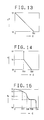
- the abscissa represents the distribution concentration C of germanium atoms and the ordinate represents the thickness of the entire photosensitive layer or the partial constituent layer adjacent to the support; and t B represents the extreme position of the photosensitive layer adjacent to the support, and t T represent the other extreme position adjacent to the surface layer which is away from the support, or the position of the interface between the constituent layer containing germanium atoms and the constituent layer not containing germanium atoms.
- the photosensitive layer containing germanium atoms is formed from the t B side toward t T side.
- Figure 7 shows the first typical example of the thicknesswise distribution of germanium atoms in the photosensitive layer.
- germanium atoms are distributed such that the concentration C is constant at a value C1 in the range from position t B (at which the photosensitive layer containing germanium atoms is in contact with the surface of the support) to position t1, and the concentration C gradually and continuously decreases from C2 in the range from position t1 to position t T at the interface.
- the concentration of germanium atoms is substantially zero at the interface position t T .
- substantially zero means that the concentration is lower than the detectable limit.
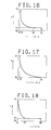
- the distribution of germanium atoms is such that concentration C5 is constant in the range from position t B and position t2 and it gradually and continuously decreases in the range from position t2 and position t T .
- concentration at position t T is substantially zero.
- the distribution of germanium atoms is such that concentration C6 gradually and continuously decreases in the range from position t B and position t3, and it sharply and continuously decreases in the range from position t3 to position t T .
- the concentration at position t T is substantially zero.
- the distribution of germanium atoms C is such that concentration C7 is constant in the range from position t B and position t4 and it linearly decreases in the range from position t4 to position t T .
- concentration at position t T is zero.
- the distribution of germanium atoms is such that concentration C8 is constant in the range from position t B and position t5 and concentration C9 linearly decreases to concentration C10 in range from position t5 to position t T .
- the distribution of germainum atoms is such that concentration linearly decreases to zero in the range from position t B to position t T .
- the distribution of germanium atoms is such that concentration C12 linearly decreases to C13 in the range from position t B to position t6 and concentration C13 remains constant in the range from position t6 to position t T .
- the distribution of germanium atoms is such that concentration C14 at position t B slowly decreases and then sharply decreases to concentration C15 in the range from position t B to position t7.
- the concentration sharply decreases at first and slowly decreases to C16 at position t8.
- the concentration slowly decreases to C17 between poistion t8 and position t9.
- Concentration C17 further decreases to substantially zero between position t9 and position t T .
- the concentration decreases as shown by the curve.
- the concentration of germanium atoms and/or tin atoms in the photosensitive layer should preferably be high at the position adjacent to the support and considerably low at the position adjacent to the interface t T .
- the photosensitive layer constituting the light receiving member of this invention have a region adjacent to the support in which germanium atoms and/or tin atoms are locally contained at a comparatively high concentration.
- Such a local region in the light receiving member of this invention should preferably be formed within 5 ⁇ m from the interface t B .
- the local region may occupy entirely or partly the thickness of 5 ⁇ m from the interface position t B .
- the local region should occupy entirely or partly the layer depends on the performance required for the light receiving layer to be formed.
- the thicknesswise distribution of germanium atoms and/or tin atoms contained in the local region should be such that the maximum concentration C max of germanium atoms and/or tin atoms is greater than l000 atomic ppm, preferably greater than 5000 atomic ppm, and more preferably greater than l ⁇ l04 atomic ppm based on the amount of silicon atoms.
- the photosensitive layer which contains germanium atoms and/or tin atoms should preferably be formed such that the maximum concentration C max of their distribution exists within 5 ⁇ m of thickness from t B (or from the support side).
- the amount of germanium atoms and/or tin atoms in the photosensitive layer should be properly determined so that the object of the invention is effectively achieved. It is usually l to 6 ⁇ l05 atomic ppm, preferably l0 to 3 ⁇ l05 atomic ppm, and more preferably l ⁇ l02 to 2 ⁇ l05 atomic ppm.
- the photosensitive layer of the light receiving member of this invention may be incorporated with at least one kind selected from oxygen atoms, carbon atoms, nitrogen atoms. This is effective in increasing the photosensitivity and dark resistance of the light receiving member and also in improving adhesion between the support and the light receiving layer.
- the photosensitive layer of the light receiving member In the case of incorporating at least one kind selected from oxygen atoms, carbon atoms, and nitrogen atoms into the photosensitive layer of the light receiving member according to this invention, it is performed at a uniform distribution or uneven distribution in the direction of the layer thickness depending on the purpose or the expected effects as described above, and accordingly, the content is varied depending on them.
- the dark resistance of the light receiving member they are contained at a uniform distribution over the entire layer region of the photosensitive layer.
- the amount of at least one kind selected from carbon atoms, oxygen atoms, and nitrogen atoms contained in the photosensitive layer may be relatively small.
- At least one kind selected from carbon atoms, oxygen atoms, and nitrogen atoms is contained unifromly in the layer constituting the photosensitive layer adjacent to the support, or at least one kind selected from carbon atoms, oxygen atoms, and nitrogen atoms is contained such that the distribution concentration is higher at the end of the photosensitive layer on the side of the support.
- the amount of at least one kind selected from oxygen atoms, carbon atoms, and nitrogen atoms is comparatively large in order to improve the adhesion to the support.
- the amount of at least one kind selected from oxygen atoms, carbon atoms, and nitrogen atoms contained in the photosensitive layer of the light receiving member according to this invention is also determined while considering the organic relationship such as the performance at the interface in contact with the support, in addition to the preformance required for the light receiving layer as described above and it is usually from 0.00l to 50 atomic%, preferably, from 0.002 to 40 atomic%, and, most suitably, from 0.003 to 30 atomic%.
- the upper limit for the content is made smaller. That is, if the thickness of the layer region incorporated with the element is 2/5 of the thickness for the photosensitive layer, the content is usually less than 30 atomic%, preferably, less than 20 atomic% and, more suitably, less than l0 atomic%.
- atoms(O,C,N) The content of at least one of the elements selected from oxygen atoms(O), carbon atoms(C) and nitrogen atoms(N) is hereinafter referred to as "atoms(O,C,N)".
- the abscissa represents the distribution concentration C of the atoms(O,C,N) and the ordinate represents the thickness of the photosensitive layer; and t B represents the interface position between the support and the photosensitive layer and t T represents the interface position between the free surface and the photosensitive layer.
- Figure l6 shows the first typical example of the thicknesswise distribution of the atoms(O,C,N) in the photosensitive layer.
- the atoms(O,C,N) are distributed in the way that the concentration C remains constant at a value C1 in the range from position t B (at which the photosensitive layer comes into contact with the support) to position t1, and the concentration C gradually and continuously decreases from C2 in the range from position t1 to position t T , where the concentration of the group III atoms or group V atoms is C3.
- the distribution concentration C of the atoms(O,C,N) contained in the photosensitive layer is such that concentration C4 at position t B continuously decreases to concentration C5 at position t T .
- the distribution concentration C of the atoms(O,C,N) is such that concentration C6 remains constant in the range from position t B and position t2 and it gradually and continuously decreases in the range from position t2 and position t T .
- the concentration at position t T is substantially zero.
- the distribution concentration C of the atoms(O,C,N) is such that concentration C8 gradually and continuously decreases in the range from position t B and position t T , at which it is substantially zero.
- the distribution concentration C of the atoms(O,C,N) is such that concentration C9 remains constant in the range from position t B to position t3, and concentration C8 linearly decreases to concentration C10 in the range from position t3 to position t T .
- the distribution concentration C of the atoms(O,C,N) is such that concentration C11 remains constant in the range from position t B and position t4 and it linearly decreases to C14 in the range from position t4 to position t T .
- the distribution concentration C of the atoms(O,C,N) is such that concentration C14 linearly decreases in the range from position t B to position t T , at which the concentration is substantially zero.
- the distribution concentration C of the atoms(O,C,N) is such that concentration C15 linearly decreases to concentration C16 in the range from position t B to position t5 and concentration C16 remains constant in the range from position t5 to position t T .
- the distribution concentration C of the atoms(O,C,N) is such that concentration C17 at position t B slowly decreases and then sharply decreases to concentration C18 in the range from position t B to position t6.
- concentration sharply decreases at first and slowly decreases to C19 at position t7.
- the concentration slowly decreases between position t7 and position t8, at which the concentration is C20.
- Concentration C20 slowly decreases to substantially zero between position t8 and position t T .
- the improvement in the adhesion of the photosensitive layer with the support can be more effectively attained by disposing a localized region where the distribution concentration of the atoms(O,C,N) is relatively higher at the portion near the side of the support, preferably, by disposing the localized region at a position within 5 ⁇ m from the interface position adjacent to the support surface.
- the localized region may be disposed partially or entirely at the end of the light receiving layer to be contained with the atoms(O,C,N) on the side of the support, which may be properly determined in accordance with the performance required for the light receiving layer to be formed.
- the amount of the atoms(O,C,N) contained in the localized region is such that the maximum value of the distribution concentration C of the atoms(O,C,N) is greater than 500 atomic ppm, preferably, greater than 800 atomic ppm, most preferably greater than l000 atomic ppm in the distribution.
- a substance for controlling the electroconductivity may be contained to the photosensitive layer in a uniformly or unevenly distributed state to the entire or partial layer region.
- impurities in the field of the semiconductor can include atoms belonging to the group III of the periodic table that provide p-type conductivity (hereinafter simply referred to as "group III atoms") or atoms belonging to the group V of the periodic table that provide n-type conductivity (hereinafter simply referred to as "group V atoms").
- group III atoms can include B (boron), Al (aluminum), Ga (gallium), In (indium), and Tl (thallium), B and Ga being particularly preferred.
- the group V atoms can include, for example, P (phosphorus), As (arsenic), Sb (antimony), and Bi (bismuth), P and Sb being particularly preferred.
- the group III or group V atoms as the substance for controlling the conductivity into the photosensitive layer of the light receiving member according to this invention, they are contained in the entire layer region or partial layer region depending on the purpose or the expected effects as described below and the content is also varied.
- the substance is contained in the entire layer region of the photosensitive layer, in which the content of group III or group V atoms may be relatively small and it is usually from l ⁇ l0 ⁇ 3 to l ⁇ l03 atomic ppm, preferably from 5 ⁇ l0 ⁇ 2 to 5 ⁇ l02 atomic ppm, and most suitably, from l ⁇ l0 ⁇ 1 to 5 ⁇ l02 atomic ppm.
- the constituting layer containing such group III or group V atoms or the layer region containing the group III or group V atoms at high concentration function as a charge injection inhibition layer. That is, in the case of incorporating the group III atoms, movement of electrons injected from the side of the support into the photosensitive layer can effectively be inhibited upon applying the charging treatment of at positive polarity at the free surface of the photosensitive layer.
- the content in this case is relatively great. Specifically, it is generally from 30 to 5 ⁇ l04 atomic ppm, preferably from 50 to l ⁇ l04 atomic ppm, and most suitably from l ⁇ l02 to 5 ⁇ l03 atomic ppm.
- the thickness (T) of the photo sensitive layer and the thickness (t) of the layer or layer region containing the group III or group V atoms adjacent to the support should be determined such that the relation t/T ⁇ 0.4 is established. More preferably, the value for the relationship is less than 0.35 and, most suitably, less than 0.3. Further, the thickness (t) of the layer or layer region is generally 3 ⁇ l0 ⁇ 3 to l0 ⁇ m, preferably 4 ⁇ l03 to 8 ⁇ m, and, most suitably, 5 ⁇ l0 ⁇ 3 to 5 ⁇ m.
- the foregoing effect that the layer region where the group III or group V atoms are distributed at a higher density can form the charge injection inhibition layer as described above more effectively, by disposing a localized region where the distribution density of the group III or group V atoms is relatively higher at the portion near the side of the support, preferably, by disposing the localized region at a position within 5 ⁇ from the interface position in adjacent with the support surface.
- the distribution state of the group III or group V atoms and the amount of the group III or group V atoms are, of course, combined properly as required for obtaining the light receiving member having performances capable of attaining a desired purpose.
- a substance for controlling the conductivity of a polarity different from that of the substance for controlling the conductivity contained in the charge injection inhibition layer may be contained in the photosensitive layer other than the charge injection inhibition layer, or a substance for controlling the conductivity of the same polarity may be contained by an amount substantially smaller than that contained in the charge inhibition layer.
- a so-called barrier layer composed of electrically insulating material may be disposed instead of the charge injection inhibition layer as the constituent layer disposed at the end on the side of the support, or both of the barrier layer and the charge injection inhibition layer may be disposed as the constituent layer.
- the material for constituting the barrier layer can include, for example, those inorganic electrically insulating materials such as Al2O3, SiO2 and Si3N4 or organic electrically insulating material such as polycarbonate.
- the surface layer l03 of the light receiving member of this invention is disposed on the photosensitive layer l02 and has the free surface l04.
- To dispose the surface layer l03 on the photosensitive layer in the light recieving member according to this invention is aimed at reducing the reflection of an incident-light and increasing the transmission rate at the free surface l04 of the light receiving member, and improving various properties such as the moisture-proofness, the property for continuous repeating use, electrical voltage withstanding property, circumstantial resistance and durability of the light receiving member.
- the material for forming the surface layer it is required to satisfy various conditions in that it can provide the excellent reflection preventive function for the layer constituted therewith, and a function of improving the various properties as described above, as well as those conditions in that it does not give undesired effects on the photoconductivity of the light receiving member, provides an adequate electronic photographic property, for example, an electric resistance over a certain level, provide an excellent solvent resistance in the case of using the liquid developing process and it does not reduce the various properties of the light receiving layer already formed.
- Those materials that can satisfy such various conditions and can be used effectively include the following two types of materials.
- amorphous material which contains silicon atoms(Si), at least one kind selected from oxygen atoms(O), carbon atoms(C) and nitrogen atoms(N), and preferably in addition to these, either hydrogen atoms(H) or halogen atoms(X).
- Si silicon atoms
- O oxygen atoms
- C carbon atoms
- N nitrogen atoms
- a-Si(O,C,N)(H,X) halogen atoms
- the other one is at least one material selected from the group consisting of inorganic fluorides, inorganic oxides, and inorganic sulfides such as MgF2, Al2O3, ZrO2, TiO2, ZnS, CeO2, CeF3, Ta2O5 , AlF3, and NaF.
- the surface layer l03 is constituted as a multi-layered structure at least comprising an abrasion-resistant layer at the outermost side and the reflection preventive layer at the inside in order to overcome the problems of the interference fringe or uneven sensitivity resulted from the uneven thickness of the surface layer. That is, in the light receiving member comprising the surface layer of the multi-layered structure, since a plurality of interfaces are resulted in the surface layer and the reflections at the respective interfaces are offset with each other and, accordingly, the reflection at the interface between the surface layer and the light sensitive layer can be decreased, the problem in the prior art that the reflection rate is changed due to the uneven thickness of the surface layer can be overcome.
- abrasion resistant layer outermost layer
- the reflection preventive layer inner layer
- the optical band gaps (Eopt) of the layer constituting the abrasion-resistant layer (outermost layer) and the reflection preventive layer (inner layer) are made different. Specifically, it is adapted such that the refractive index of the abrasion-resistant layer (outermost layer), the refractive index of the reflection preventive layer (inner layer) and the refractive index of the light sensitive layer to which the surface layer is disposed directly are made different from each other.
- the reflection at the interface between the light sensitive layer and the surface layer can be reduced to zero by satisfying the relationship represented by the following equation : wherein n1 is the refractive index of the photosensitive layer, n2 is a refractive index of the abrasion-resistant layer constituting the surface layer, n3 is a refractive index of the reflection preventive layer, d is a thickness of the reflection preventive layer and ⁇ is the wavelength of the incident light.
- n1 ⁇ n3 ⁇ n2 in the embodiment described above, the relation is not always limited only thereto but it may, for example, be defined as n1 ⁇ n2 ⁇ n3.
- the refractive indexes are made different by making the amount of oxygen atoms, carbon atoms or hydrogen atoms contained in the surface layer different between the abrasion-resistant layer and the reflection preventive layer.
- the amount of the carbon atoms contained in the abrasion-resistant layer is made greater than the amount of the carbon atoms contained in the reflection preventive layer and the refractive index n1 of the light sensitive layer, the refractive index n3 of the reflection preventive layer, the refractive index n2 of the abrasion-resistant layer and the thickness d of the abrasion-resistant layer are made as : n1 ⁇ 2.0, n2 ⁇ 3.5, n3 ⁇ 2.65 and d ⁇ 755 ⁇ respectively.
- the refractive indexes in each of the layers can be made different.
- the abrasion-resistant layer can be formed with a-SiC(H,X) and the reflection preventive layer can be formed with a-SiN(H,X) or a-SiO(H,X).
- At least one of the elements selected from the oxygen atoms, carbon atoms and nitrogen atoms is contained in a uniformly distributed state in the abrasion-resistant layer and the reflection preventive layer constituting the surface layer.
- the foregoing various properties can be improved along with the increase in the amount of these atoms contained. However, if the amount is excessive, the layer quality is lowered and the electrical and mechanical properties are also degraded.
- the amount of these atoms contained in the surface layer is defined as usually from 0.00l to 90 atm %, preferably, from l to 90 atm % and, most suitably, from l0 to 80 atm %.
- the axount of the hydrogen atoms(H), the amount of the halogen atoms(X) or the sum of the amounts of the hydrogen atoms and the halogen atoms (H+X) contained in the surface layer is usually from l to 40 atm %, preferably, from 5 to 30 atm % and, most suitably, from 5 to 25 atm %.
- the surface layer with at least one of the compounds selected from the inorganic fluorides, inorganic oxides and inorganic sulfides, they are selectively used such that the refractive indexes in each of the light sensitive layer, the abrasion-resistant layer and the reflection preventive layer are different and the foregoing conditions can be satisfied while considering the refractive indexes for each of the inorganic compound exempliefied above and the mixture thereof.
- Numerical values in the parentheses represent the refractive indexes of the inorganic compounds and the mixtures thereof.
- the thickness of the surface layer is one of the important factors for effectively attaining the purpose of this invention and the thickness is properly determined depending on the desired purposes. It is required that the thickness be determined while considering the relative and organic relationships depending on the amount of the oxygen atoms, carbon atoms, nitrogen atoms, halogen atoms and hydrogen atoms contained in the layer or the properties required for the surface layer. Further, the thickness has to be determined also from economical point of view such as the productivity.and the mass productivity. In view of the above, the thickness of the surface layer is usually from 3 ⁇ l0 ⁇ 3 to 30 ⁇ , more preferably, from 4 ⁇ l0 ⁇ 3 to 20 ⁇ and, most preferably, 5 ⁇ l0 ⁇ 3 to l0 ⁇ .
- the light receiving member according to this invention has a high photosensitivity in the entire visible ray region and, further, since it is excellent in the photosensitive property on the side of the longer wavelength, it is suitable for the matching property, particularly, with a semiconductor laser, exhibits a rapid optical response and shows more excellent electrical, optical and electroconductive nature, electrical voltage withstand property and resistance to working circumstances.
- the light receiving member in the case of applying the light receiving member to the electrophotography, it gives no undesired effects at all of the residual potential to the image formation, stable electrical properties high sensitivity and high S/N ratio, excellent light fastness and property for repeating use, high image density and clear half tone and can provide high quality image with high resolution power repeatingly.
- the amorphous material constituting the light receiving layer in this invention is prepared by vacuum deposition technique utilizing the discharging phenomena such as glow discharging, sputtering, and ion plating process. These production processes are properly used selectively depending on the factors such as the manufacturing conditions, the installation cost required, production scale and properties required for the light receiving members to be prepared.
- the glow discharging process or sputtering process is suitable since the control for the condition upon preparing the light receiving members having desired properties are relatively easy and carbon atoms and hydrogen atoms can be introduced easily together with silicon atoms.
- the glow discharging process and the sputtering process may be used together in one identical system.
- a layer constituted with a-Si(H,X) is formed, for example, by the glow discharging process, gaseous starting material for supplying Si capable of supplying silicon atoms(Si) are introduced together with gaseous starting material for introducing hydrogen atoms(H) and/or halogen atoms(X) into a deposition chamber the inside pressure of which can be reduced, glow discharge is geenrated in the deposition chamber, and a layer composed of a-Si(H,X) is formed on the surface of a predetermined support disposed previously at a predetermined position in the chamber.
- the gaseous starting material for supplying Si can include gaseous or gasifiable silicon hydrides (silanes) such as SiH4, Si2H6, Si3H8, Si4H10, etc., SiH4 and Si2H6 being particularly preferred in view of the easy layer forming work and the good efficiency for the supply of Si.
- silanes gaseous or gasifiable silicon hydrides
- halogen compounds can be mentioned as the gaseous starting material for introducing the halogen atoms and gaseous or gasifiable halogen compounds, for example, gaseous halogen, halides, inter-halogen compounds and halogen-substituted silane derivatives are preferred.
- gaseous halogen, halides, inter-halogen compounds and halogen-substituted silane derivatives are preferred.
- they can include halogen gas such as of fluorine, chlorine bromine, and iodine; inter-halogen compounds such as BrF, ClF, ClF3, BrF2, BrF3, IF7, ICl, IBr, etc.; and silicon halides such as SiF4, Si2H6, SiCl4, and SiBr4.
- the use of the gaseous or gasifiable silicon halide as described above is particularly advantageous since the layer constituted with halogen atom-containing a-Si can be formed with no additional use of the gaseous starting
- the gaseous starting material usable for supplying hydrogen atoms can include those gaseous or gasifiable materials, for example, hydrogen gas, halides such as HF, HCl, HBr, and HI, silicon hydrides such as SiH4, Si2H6, Si3H8, and Si4O10, or halogen-substituted silicon hydrides such as SiH2F2, SiH2I2, SiH2Cl2, SiHCl3, SiH2Br2, and SiHBr3.
- the use of these gaseous starting material is advantageous since the content of the hydrogen atoms(H), which are extremely effective in view of the control for the electrical or photoelectronic properties, can be controlled with ease.
- the use of the hydrogen halide or the halogen-substituted silicon hydride as described above is particularly advantageous since the hydrogen atoms(H) are also introduced together with the introduction of the halogen atoms.
- the halogen atoms are introduced by introducing gaseous halogen compounds or halogen atom-containing silicon compounds into a deposition chamber thereby forming a plasma atmosphere with the gas.
- the gaseous starting material for introducing the hydrogen atoms for example, H2 or gaseous silanes are described above are introduced into the sputtering deposition chamber thereby forming a plasma atmosphere with the gas.
- a layer comprising a-Si(H,X) is formed on the support by using a Si target and by introducing a halogen atom-introducing gas and H2 gas together with an inert gas such as He or Ar as required into a deposition chamber thereby forming a plasma atmosphere and then sputtering the Si target.
- a feed gas to liberate silicon atoms(Si), a feed gas to liberate germanium atoms(Ge), and a feed gas to liberate hydrogen atoms(H) and/or halogen atoms(X) are introduced under appropriate gaseous pressure condition into an evacuatable deposition chamber, in which the glow discharge is generated so that a layer of a-SiGe(H,X) is formed on the properly positioned support in the chamber.
- the feed gases to supply silicon atoms, halogen atoms, and hydrogen atoms are the same as those used to form the layer of a-Si(H,X) mentioned above.
- the feed gas to liberate Ge includes gaseous or gasifiable germanium halides such as GeH4, Ge2H6, Ge3H8, Ge4H10, Ge5H12, Ge6H14, Ge7H16, Ge8H18, and Ge9H20, with GeH4, Ge2H6 and Ge3H8, being preferable on account of their ease of handling and the effective liberation of germanium atoms.
- gaseous or gasifiable germanium halides such as GeH4, Ge2H6, Ge3H8, Ge4H10, Ge5H12, Ge6H14, Ge7H16, Ge8H18, and Ge9H20, with GeH4, Ge2H6 and Ge3H8, being preferable on account of their ease of handling and the effective liberation of germanium atoms.
- a-SiGe(H,X) To form the layer of a-SiGe(H,X) by the sputtering process, two targets (a silicon target and a germanium target) or a single target composed of silicon and germanium is subjected to sputtering in a desired gas atmosphere.
- the vapors of silicon and germanium are allowed to pass through a desired gas plasma atmosphere.
- the silicon vapor is produced by heating polycrystal silicon or single crystal silicon held in a boat
- the germanium vapor is produced by heating polycrystal germanium or single crystal germanium held in a boat. The heating is accomplished by resistance heating or electron beam method (E.B. method).
- the layer may be incorporated with halogen atoms by introducing one of the above-mentioned gaseous halides or halogen-containing silicon compounds into the deposition chamber in which a plasma atmosphere of the gas is produced.
- a feed gas to liberate hydrogen is introduced into the deposition chamber in which a plasma atmosphere of the gas is produced.
- the feed gas may be gaseous hydrogen, silanes, and/or germanium hydride.
- the feed gas to liberate halogen atoms includes the above-mentioned halogen-containing silicon compounds.
- feed gas examples include hydrogen halides such as HF, HCl, HBr, and HI; halogen-substituted silanes such as SiH2F2, SiH2I2, SiH2CI2, SiHCl3, SiH2Br2, and SiHBr3; germanium hydride halide such as GeHF3, GeH2F2, GeH3F, GeHCl3, GeH2Cl2, GeH3Cl, GeHBr3, GeH2Br2, GeH3Br, GeHI3, GeH2I2, and GeH3I; and germanium halides such as GeF4, GeCl4, GeBr4, GeI4, GeF2, GeCl2, GeBr2, and GeI2. They are in the gaseous form or gasifiable substances.
- hydrogen halides such as HF, HCl, HBr, and HI
- halogen-substituted silanes such as SiH2F2, SiH2I2, SiH2CI2, SiHCl3, SiH2Br2,
- a starting material (feed gas) to release tin atoms(Sn) is used in place of the starting material to release germanium atoms which is used to form the layer composed of a-SiGe(H,X) as mentioned above.
- the process is properly controlled so that the layer contains a desired amount of tin atoms.
- Examples of the feed gas to release tin atoms(Sn) include tin hydride (SnH4) and tin halides (such as SnF2, SnF4, SnCl2, SnCl4, SnBr2, SnBr4, SnI2, and SnI4) which are in the gaseous form or gasifiable.
- Tin halides are preferable because they form on the substrate a layer of a-Si containing halogen atoms.
- SnCl4 is particularly preferable because of its ease of handling and its efficient tin supply.
- solid SnCl4 is used as a starting material to supply tin atoms(Sn), it should preferably be gasified by blowing (bubbling) an inert gas (e.g., Ar and He) into it while heating.
- an inert gas e.g., Ar and He
- the gas thus generated is introduced, at a desired pressure, into the evacuated deposition chamber.
- the layer may be formed from an amorphous material [a-Si(H,X) or a-Si(Ge,Sn)(H,X)] which further contains the group III atoms or group V atoms, nitrogen atoms, oxygen atoms, or carbon atoms, by the glow-discharge process, sputtering process, or ion-plating process.
- a-Si(H,X) or a-Si(Ge,Sn) (H,X) is used in combination with the starting materials to introduce the group III atoms or group V atoms, nitrogen atoms, oxygen atoms, or carbon atoms.
- the supply of the starting materials should be properly controlled so that the layer contails a desired amount of the necessary atoms.
- the layer is to be formed by the glow-discharge process from a-Si(H,X) containing atoms(O,C,N) or from a-Si(Ge,Sn)(H,X) containing atoms(O,C,N)
- the starting material to form the layer of a-Si(H,X) or a-Si(Ge,Sn)(H,X) should be combined with the starting material used to introduce atoms(O,C,N).
- the supply of these starting materials should be properly controlled so that the layer contains a desired amount of the necessary atoms.
- the starting material to introduce the atoms(O,C,N) may be any gaseous substance or gasifiable substance composed of any of oxygen, carbon, and nitrogen.
- Examples of the starting materials used to introduce oxygen atoms(O) include oxygen (O2), ozone (O3), nitrogen dioxide (NO2), nitrous oxide (N2O), dinitrogen trioxide (N2O3), dinitrogen tetroxide (N2O4), dinitrogen pentoxide (N2O5), and nitrogen trioxide (NO3).
- H3SiOSiH3 disiloxane
- H3SiOSiH2OSiH3 trisiloxane
- Examples of the starting materials used to introduce carbon atoms include saturated hydrocarbo s having l to 5 carbon atoms such as methane (CH4), ethane (C2H6), propane (C3H8), n-butane (n-C4H10), and pentane (C5H12); ethylenic hydrocarbons having 2 to 5 carbon atoms such as ethylene (C2H4), propylene (C3H6), butene-l (C4H8), butene-2 (C4H8), isobutylene (C4H8), and pentene (C5H10); and acetylenic hydrocarbons having 2 to 4 carbon atoms such as acetylene (
- Examples of the starting materials used to introduce nitrogen atoms include nitrogen (N2), ammonia (NH3), hydrazine (H2NNH2), hydrogen azide (HN3), ammonium azide (NH4N3), nitrogen trifluoride (F3N), and nitrogen tetrafluoride (F4N).
- the starting material for introducing the group III or group V atoms are used together with the starting material for forming a-Si(H,X) or a-Si(Ge,Sn)(H,X) upon forming the layer constituted with a-Si(H,X) or a-Si(Ge,Sn)(H,X) as described above and they are incorporated while controlling the amount of them into the layer to be formed.
- the boron atoms introducing materials can include boron hydrides such as B2H6, B4H10, B5H9, B5H11, B6H10, B6H12, and B6H14, and boron halides such as BF4, BCl3, and BBr3
- boron hydrides such as B2H6, B4H10, B5H9, B5H11, B6H10, B6H12, and B6H14
- boron halides such as BF4, BCl3, and BBr3
- AlCl3, CaCl3, Ga(CH3)2, InCl3, TlCl3, and the like can also be mentioned.
- the starting material for introducing the group V atoms and, specifically, to the phosphorus atom introducing materials can include, for example, phosphorus hydrides such as PH3 and P2H6 and phosphorus halides such as PH4I, PF3, PF5, PCl3, PCl5, PBr3, PBr5, and PI3.
- AsH3, AsF5, AsCl3, AsBr3, AsF3, SbH3, SbF3, SbF5, SbCl3, SbCl5, BiH3, BiCl3, and BiBr3 can also be mentioned to as the effective starting material for introducing the group V atoms.
- starting material for introducing the oxygen atoms is added to those selected from the group of the starting material as described above for forming the light receiving layer.
- the starting material for introducing the oxygen atoms most of those gaseous or gasifiable materials can be used that comprise at least oxygen atoms as the constituent atoms.
- gaseous starting material comprising silicon atoms(Si) as the constituent atoms
- gaseous starting material comprising oxygen atoms(O)
- gaseous starting material comprising hydrogen atoms(H) and/or halogen atoms(X) as the constituent atoms in a desired mixing ratio
- a mixture of gaseous starting material comprisinging silicon atoms(Si) as the constituent atoms and gaseous starting material comprising oxygen atoms(O) and hydrogen atoms(H) as the constituent atoms in a desired mixing ratio
- a mixture of gaseous starting material comprising silicon atoms(Si) as the constituent atoms and gaseous starting material comprising silicon atoms(Si), oxygen atoms(O) and hydrogen atoms(H) as the constituent atoms.
- gaseous starting material comprising silicon atoms(si) and hydrogen atoms(H) as the constituent atoms and gaseous starting material comprising oxygen atoms(O) as the constituent atoms.
- oxygen O2
- ozone O3
- nitrogen monoxide NO
- NO2 nitrogen dioxide
- N2O dinitrogen oxide
- N2O3 dinitrogen trioxide
- N2O4 dinitrogen pentaxide
- NO3 nitrogen trioxide
- lower siloxanes comprising silicon atoms(Si)
- the layer or layer region containing oxygen atoms by way of the sputtering process, it may be carried out by sputtering a single crystal or polycrystalline Si wafer or SiO2 wafer, or a wafer containing Si and SiO2 in admixture is used as a target and sputtered in various gas atmospheres.
- a gaseous starting material for introducing oxygen atoms and, optionally, hydrogen atoms and/or halogen atoms is diluted as required with a dilution gas, introduced into a sputtering deposition chamber, gas plasmas with these gases are formed and the Si wafer is sputtered.
- sputtering may be carried out in the atmosphere of a dilution gas or in a gas atmosphere containing at least hydrogen atoms(H) and/or halogen atoms(X) as constituent atoms as a sputtering gas by using individually Si and SiO2 targets or a single Si and SiO2 mixed target.
- the gaseous starting material for introducing the oxygen atoms the gaseous starting material for introducing the oxygen atoms as mentioned in the examples for the glow discharging process as described above can be used as the effective gas also in the sputtering.
- gaseous starting materials that are effectively usable herein can include gaseous silicon hydrides comprising C and H as the constituent atoms, such as silanese, for example, SiH4, Si2H6, Si3H8 and Si4H10, as well as those comprising C and H as the constituent atoms, for example, saturated hydrocarbons of l to 4 carbon atoms, ethylenic hydrocarbons of 2 to 4 carbon atoms and acetylenic hydrocarbons of 2 to 3 carbon atoms.
- silanese for example, SiH4, Si2H6, Si3H8 and Si4H10
- those comprising C and H as the constituent atoms for example, saturated hydrocarbons of l to 4 carbon atoms, ethylenic hydrocarbons of 2 to 4 carbon atoms and acetylenic hydrocarbons of 2 to 3 carbon atoms.
- the saturated hydrocarbons can include methane (CH4), ethane (C2H6), propane (C3H8), n-butane (n-C4H10) and pentane (C5H12),
- the ethylenic hydrocarbons can include ethylene (C2H4), propylene (C3H6), butene-l (C4H8), butene-2 (C4H8), isobutylene (C4H8) and pentene (C5H10)
- the acetylenic hydrocarbons can include acetylene (C2H2), methylacetylene (C3H4) and butine (C4H6).
- the gaseous starting material comprising Si, C and H as the constituent atoms can include silicified alkyls, for example, Si(CH3)4 and Si(C2H5)4.
- H2 can of course be used as the gaseous starting material for introducing H.
- the layer composed of a-SiC(H,X) is carried out by using a single crystal or polycrystalline Si wafer, a C (graphite) wafer or a wafer containing a mixture of Si and C as a target and sputtering them in a desired gas atmosphere.
- gaseous starting material for introducing carbon atoms, and hydrogen atoms and/or halogen atoms is introduced while being optionally diluted with a dilution gas such as Ar and He into a sputtering deposition chamber thereby forming gas plasmas with these gases and sputtering the Si wafer.
- a dilution gas such as Ar and He
- gaseous starting material for introducing hydrogen atoms and/or halogen atoms as the sputtering gas is optionally diluted with a dilution gas, introduced into a sputtering deposition chamber thereby forming gas plasmas and sputtering is carried out.
- gaseous starting material for introducing each of the atoms used in the sputtering process those gaseous starting materials used in the glow discharging process as described above may be used as they are.
- starting material for introducing nitrogen atoms is added to the material selected as required from the starting materials for forming the light receiving layer as described above.
- the starting material for introducing the nitrogen atoms most of gaseous or gasifiable materials can be used that comprise at least nitrogen atoms as the constituent atoms.
- gaseous starting material comprising silicon atoms(Si) as the constituent atoms
- gaseous starting material comprising nitrogen atoms(N) as the constituent atoms
- gaseous starting material comprising hydrogen atoms(H) and/or halogen atoms(X) as the constituent atoms mixed in a desired mixing ratio
- a mixture of starting gaseous material comprising silicon atoms(Si) as the constituent atoms and gaseous starting material comprising nitrogen atoms(N) and hydrogen atoms(H) as the constituent atoms also in a desired mixing ratio.
- gaseous starting material comprising nitrogen atoms(N) as the constituent atoms gaseous starting material comprising silicon atoms(Si) and hydrogen atoms(H) as the constituent atoms.
- the starting material that can be used effectively as the gaseous starting material for introducing the nitrogen atoms(N) used upon forming the layer or layer region containing nitrogen atoms can include gaseous or gasifiable nitrogen, nitrides and nitrogen compounds such as azide compounds comprising N as the constituent atoms or N and H as the constituent atoms, for example, nitrogen (N2), ammonia (NH3), hydrazine (H2NNH2), hydrogen azide (HN3) and ammonium azide (NH4N3).
- nitrogen halide compounds such as nitrogen trifluoride (F3N) and nitrogen tetrafluoride (F4N2) can also be mentioned in that they can also introduce halogen atoms(X) in addition to the introduction of nitrogen atoms(N).
- the layer or layer region containing the nitrogen atoms may be formed through the sputtering process by using a single crystal or polycrystalline Si wafer or Si3N4 wafer or a wafer containing Si and Si3N4 in admixture as a target and sputtering them in various gas atmospheres.
- gaseous starting material for introducing nitrogen atoms and, as required, hydrogen atoms and/or halogen atoms is diluted optionally with a dilution gas, introduced into a sputtering deposition chamber to form gas plasmas with these gases and the Si wafer is sputtered.
- Si and Si3N4 may be used as individual targets or as a single target comprising Si and Si3N4 in admixture and then sputtered in the atmosphere of a dilution gas or in a gaseous atmosphere containing at least hydrogen atoms(H) and/or halogen atoms(X) as the constituent atoms as for the sputtering gas.
- a gaseous atmosphere containing at least hydrogen atoms(H) and/or halogen atoms(X) as the constituent atoms as for the sputtering gas.
- the gaseous starting material for introducing nitrogen atoms those gaseous starting materials for introducing the nitrogen atoms described previously as mentioned in the example of the glow discharging as above described can be used as the effective gas also in the case of the sputtering.
- the light receiving layer of the light receiving member of this invention is produced by the glow discharge process or sputtering process.
- the amount of germanium atoms and/or tin atoms; the group III atoms or group V atoms; oxygen atoms, carbon atoms, or nitrogen atoms; and hydrogen atoms and/or halogen atoms in the light receiving layer is controlled by regulating the gas flow rate of each of the starting materials or the gas flow ratio among the starting materials respectively entering the deposition chamber.
- the conditions upon forming the photosensitive layer and the surface layer of the light receiving member of the invention for example, the temperature of the support, the gas pressure in the deposition chamber, and the electric discharging power are important factors for obtaining the light receiving member having desired properties and they are properly selected while considering the functions of the layer to be made. Further, since these layer forming conditions may be varied depending on the kind and the amount of each of the atoms contained in the light receiving layer, the conditions have to be determined also taking the kind or the amount of the atoms to be contained into consideration.
- the temperature of the support is usually from 50 to 350°C and, more preferably, from 50 to 250°C;
- the gas pressure in the deposition chamber is usually from 0.0l to l Torr and, particularly preferably, from 0.l to 0.5 Torr;
- the electrical discharging power is usually from 0.005 to 50 W/cm2, more preferably, from 0.0l to 30 W/cm2 and, particularly preferably, from 0.0l to 20 W/cm2.
- the temperature bf the support is usually from 50 to 350°C, more preferably, from 50 to 300°C, most preferably l00 to 300°C;
- the gas pressure in the deposition chamber is usually from 0.0l to 5 Torr, more preferably, from 0.00l to 3 Torr, most preferably from 0.l to l Torr;
- the electrical discharging power is usually from 0.005 to 50 W/cm2, more preferably, from 0.0l to 30 W/cm2, most preferably, from 0.0l to 20 W/cm2.
- the actual conditions for forming the layer such as temperature of the support, discharging power and the gas pressure in the deposition chamber cannot usually be determined with ease independent of each other.
- the conditions optimal to the layer formation are desirably determined based on relative and organic relationships for forming the amorphous material layer having desired properties.
- the layer is formed, for example, in the case of the glow discharging process, by properly varying the gas flow rate of gaseous starting material for introducing germanium atoms and/or tin atoms, oxygen atoms, carbon atoms, nitrogen atoms, or the group III atoms or group V atoms upon introducing into the deposition chamber in accordance with a desired variation coefficient while maintaining other conditions constant.
- the gas flow rate may be varied, specifically, by gradually changing the opening degree of a predetermined needle valve disposed to the midway of the gas flow system, for example, manually or any of other means usually employed such as in externally driving motor.
- the variation of the flow rate may not necessarily be linear but a desired content curve may be obtained, for example, by controlling the flow rate along with a previously designed variation coefficient curve by using a microcomputer or the like.
- a desired distributed state of the germanium atoms and/or tin atoms, oxygen atoms, carbon atoms, nitrogen atoms, or the group III atoms or group V atoms in the direction of the layer thickness may be formed with the distribution density being varied in the direction of the layer thickness by using gaseous starting material for introducing the germanium atoms and/or tin atoms, oxygen atoms, carbon atoms, nitrogen atoms, or the group III atoms or group V atoms and varying the gas flow rate upon introducing these gases into the deposition chamber in accordance with a desired variation coefficient in the same manner as the case of using the glow discharging process.
- the surface layer in this invention with at least one of the elements selected from the inorganic fluorides, inorganic oxides and inorganic sulfides, since it is also necessary to control the layer thickness at an optical level for forming such a surface layer, vapor deposition, sputtering, gas phase plasma, optical CVD, heat CVD process or the like may be used. These forming processes are, of course, properly selected while considering those factors such as the kind of the forming materials for the surface layer, production conditions, installation cost required and production scale.
- sputtering process may preferably be employed in the case of using the inorganic compounds for forming the surface layer. That is, the inorganic compound for forming the surface layer is used as a target and Ar gas is used as a sputtering gas, and the surface layer is deposited by causing glow discharging and sputtering the inorganic compounds.
- the photosensitive layer was formed by using the glow discharging process and the surface layer was formed by using the glow discharging process or the sputtering process.
- Figure 25 shows an apparatus for preparing a light receiving member according to this invention by means of the glow discharging process.
- Gas reservoirs 2502, 2503, 2504, 2505, and 2506 illustrated in the figure are charged with gaseous starting materials for forming the respective layers in this invention, that is, for instance, SiF4 gas (99.999% purity) in gas reservoir 2505, B2H6 gas (99.999% purity) diluted with H2 (referred to as B2H6/H2) in gas reservoir 2503, CH4 gas (99.999% purity) in gas reservoir 2504, GeF4 gas (99.999% purity) in gas reservoir 2505, and inert gas (He) in gas resorvoir 2506. SnCl4 is held in a closed container 2506′.
- valves 2522 - 2526 for the gas cylinders 2502 - 2506 and a leak valve l935 are closed and that inlet valves 25l2 - 25l6, exit valves 25l7 - 252l, and sub-valves 2532 and 2533 are opened.
- a main valve 2534 is at first opened to evacuate the inside of the reaction chamber 250l and gas piping.
- SiH4 gas from the gas reservoir 2502, B2H6/H2 gas form the gas resorvoir 2503, and GeF4 gas from the gas reservoir 2505 are caused to flow into mass flow controllers 2507, 2508, and 25l0 respectively by opening the inlet valves 25l2, 25l3, and 25l5, controlling the pressure of exit pressure gauges 2527, 2528, and 2530 to l kg/cm2. Subsequently, the exit valves 25l7, 25l8, and 2520, and the sub-valve 2532 are gradually opened to enter the gases into the reaction chamber 250l.
- the exit valves 25l7, 25l8, and 2520 are adjusted so as to attain a desired value for the ratio among the SiF4 gas flow rate, GeF4 gas flow rate, and B2H6/H2 gas flow rate, and the opening of the main valve 2534 is adjusted while observing the reading on the vacuum gauge 2536 so as to obtain a desired value for the pressure inside the reaction chamber 250l.
- a power source 2540 is set to a predetermined electrical power to cause glow discharging in the reaction chamber 250l while controlling the flow rates of SiF4 gas, GeF4 gas, and B2H4/H2 gas in accordance with a previously designed variation coefficient curve by using a microcomputer (not shown), thereby forming, at first, the first layer containing silicon atoms, germanium atoms, and boron atoms on the substrate cylinder 2537.
- the exit valves 25l8 and 2520 are completely closed, and the glow discharge is continued in the same manner except that the discharge conditions are changed as required, whereby the second layer is formed on the first layer.
- SiF4 gas and CH4 gas are optionally diluted with a dilution gas such as He, Ar and H2 respectively, entered at a desired gas flow rates into the reaction chamber 250l while controlling the gas flow rate for the SiF4 gas and the CH4 gas in accordance with a previously designed variation coefficient curve by using a microcomputer and glow discharge being caused in accordance with predetermined conditions, by which a surface layer constituted with a-Si(H,X) containing carbon atoms is formed.
- a dilution gas such as He, Ar and H2 respectively
- All of the exit valves other than those required for upon forming the respective layers are of course closed. Further, upon forming the respective layers, the inside of the system is onceevacuated to a high vacuum degree as required by closing the exit valves 25l7 - 252l while opening the sub-valves 2532 and 2533 and fully opening the main valve 2534 for avoiding that the gases having been used for forming the previous layers are left in the reaction chamber 250l and in the gas pipeways from the exit valves 25l7 - 252l to the inside of the reaction chamber 250l.
- the starting material for tin atoms, solid SnCl4 placed in 2506′ is heated by a heating means (not shown) and an inert gas such as He is blown for bubbling from the inert gas reservoir 2506.
- an inert gas such as He is blown for bubbling from the inert gas reservoir 2506.
- the thus generated gas of SnCl4 is introduced into the reaction chamber in the same manner as mentioned for SiF4 gas, GeF4 gas, CH4 gas, and B2H6/H2 gas.
- the valves for the feed gases and diluent gas used for the layer of amorphous material are closed, and then the leak valve 2535 is gradually opened so that the pressure in the deposition chamber is restored to the atmospheric pressure and the deposition chamber is scavenged with argon gas.
- a target of the inorganic material for the formation of the surface layer is spread all over the cathode (not shown), and the deposition chamber is evacuated, with the leak valve 2535 closed, and argon gas is introduced into the deposition chamber until a pressure of 0.0l5 to 0.02 Torr is reached.
- a high-frequency power (l50 to l70 W) is applied to bring about glow discharge, whereby sputtering the inorganic material so that the surface layer is deposited on the previously formed layer.
- Rigid spheres of 0.6 mm diameter made of SUS stainless steels were chemically etched to form an unevenness to the surface of each of the rigid spheres.
- etching agent Usable as the etching agent are an acid such as hydrochloric acid, hydrofluoric acid, sulfuric acid and chromic acid and an alkali such as caustic soda.
- an aqueous solution prepared by admixing l.0 volumetric part of concentrated hydrochloric acid to l.0 to 4.0 volumetric part of distilled water was used, and the period of time for the rigid spheres to be immersed in the aqueous solution, the acid concentration of the aqueous solution and other necessary conditions were appropriately adjusted to form a desired unevenness to the surface of each of the rigid spheres.
- the radius of curvature R and the width D of the dimple was determined depending on the conditions such as the diameter R′ for the rigid sphere, the falling height h and the like. It was also confirmed that the pitch between each of the dimples (density of the dimples or the pitch for the unevenness) could be adjusted to a desired pitch by controlling the rotating speed or the rotation number of the cylinder, or the falling amount of the rigid sphere.
- R the magnitude of R and of D
- R it is not preferred for R to be less than 0.l mm because the rigid spheres to be employed in that case are to be lighter and smaller, that results in making it difficult to control the formation of the dimples as expected.
- R it is not preferred for R to be more than 2.0 mm because the rigid spheres to be employed in that case are to be heavier and the falling height is to be extremely lower, for instance, in the case where D is desired to be relatively smaller in order to adjust the falling height, that results in making it also difficult to control the formation of the dimples as expected.
- D is not preferred for D to be less than 0.02 mm because the rigid spheres to be employed in that case are to be of a smaller size and to be lighter in order to secure their falling height, that results in making it also difficult to control the formation of the dimples as expected. Further in addition, when examining the dimples as formed, it was confirmed that the insdie face of each of the dimples as formed was provided with appropriate minute irregularities.
- the surface of an aluminum alloy cylinder was fabricated in the same manner as in the Test Example 2 to obtain a cylindrical Al support having diameter D and ratio D/R (cylinder Nos. l0l to l06) shown in the upper column of Table lA.
- These light receiving members were subjected to imagewise exposure by irradiating laser beams at 780 nm wavelength and with 80 ⁇ m spot diameter using an image exposing device shown in Figure 26 and images were obtained by subsequent development and transfer.
- the state of the occurrence of interference fringe on the thus obtained images were as shown in the lower row of Table lA.
- Figure 26(A) is a schematic plan view illustrating the entire exposing device
- Figure 26(B) is a schematic side elevational view for the entire device.
- a light receiving member 260l is shown, a semiconductor laser 2602, an f ⁇ lens 2603, and a polygonal mirror 2604.
- a light receiving member was manufactured in the same manner as described above by using an aluminum alloy cylinder (No. l07), the surface of which was fabricated with a conventional cutting tool (60 mm in diameter, 298 mm in length, l00 ⁇ m unevenness pitch, and 3 ⁇ m unevenness depth).
- a conventional cutting tool 60 mm in diameter, 298 mm in length, l00 ⁇ m unevenness pitch, and 3 ⁇ m unevenness depth.
- a light receiving layer was formed on each of the Al supports (cylinder Nos. l0l to l07) in the same manner as in Example l except for forming these light receiving layers in accordance with the layer forming conditions as shown in Tables A and B.
- a light receiving layer was formed on each of the Al supports (Cylinder Nos. l03 to l06) in the same manner as in Example l except for forming these light receiving layers in accordance with the layer forming conditions shown in Tables A and B.
Landscapes
- Physics & Mathematics (AREA)
- General Physics & Mathematics (AREA)
- Chemical & Material Sciences (AREA)
- Inorganic Chemistry (AREA)
- Photoreceptors In Electrophotography (AREA)
- Light Receiving Elements (AREA)
- Inspection Of Paper Currency And Valuable Securities (AREA)
Abstract
Description
- This invention concerns light receiving members being sensitive to electromagnetic waves such as light (which herein means in a broader sense those lights such as ultra-violet rays, visible rays, infrared rays, X-rays, and Y-rays). More specifically, the invention relates to improved light receiving members suitable particularly for use in the case where coherent lights such as laser beams are applied.
- For the recording of digital image information, there has been known such a method as forming electrostatic latent images by optically scanning a light receiving member with laser beams modulated in accordance with the digital image information, and then developing the latent images or further applying transfer, fixing or like other treatment as required. Particularly, in the method of forming images by an Electro-photographic process, image recording has usually been conducted by using a He-Ne laser or a semiconductor laser (usually having emission wavelength at from 650 to 820 nm), which is small in size and inexpensive in cost as the laser source.
- By the way, as the light receiving members for electro-photography being suitable for use in the case of using the semiconductor laser, those light receiving members comprising amorphous materials containing silicon atoms (hereinafter referred to as "a-Si"), for example, as disclosed in Japanese Patent Laid-Open Nos. 8634l/l979 and 83746/l98l, have been evaluated as being worthy of attention since they have a high Vickers hardness and cause less problems in the public pollution, in addition to their excellent matching property in the photosensitive region as compared with other kinds of known light receiving members.
- However, when the light receiving layer constituting the light receiving member as described above is formed as an a-Si layer of mono-layer structure, it is necessary to structurally incorporate hydrogen or halogen atoms or, further, boron atoms within a range of specific amount into the layer in order to maintain the required dark resistance of greater than l0¹² Ωcm as for the electrophotography while maintaining their high photosensitivity. Therefore, the degree of freedom for the design of the light receiving member undergoes a rather severe limit such as the requirement for the strict control for various kinds of conditions upon forming the layer. Then, there have been made several proposals to overcome such problems for the degree of freedom in view of the design in that the high photosensitivity can effectively be utilized while reducing the dark resistance to some extent. That is, the light receiving layer is so constituted as to have two or more layers prepared by laminating those layers for different conductivity in which a depletion layer is formed to the inside of the light receiving layer as disclosed in Japanese Patent Laid-Open Nos. l7l743/l979, 4053/l982, and 4l72/l982, or the apparent dark resistance is improved by providing a multi-layered structure in which a barrier layer is disposed between the support and the light receiving layer and/or on the upper surface of the light receiving layer as disclosed, for example, in Japanese Patent Laid-Open Nos. 52l78/l982, 52l79/l982, 52l80/l982, 58l59/l982, 58l60/l982, and 58l6l/l982.
- However, such light receiving members as having a light receiving layer of multi-layered structure have unevenness in the thickness for each of the layers. In the case of conducting the laser recording by using such members, since the laser beams comprise coherent monochromatic light, the respective reflection lights reflected from the free surface of the light receiving layer on the side of the laser beam irradiation and from the layer boundary between each of the layers constituting the light receiving layer and between the support and the light receiving layer (hereinafter both of the free surface and the layer interface are collectively referred to as "interface") often interfere with each other.
- The interference results in a so-called interference fringe pattern in the formed images which brings about defective images. Particularly, in the case of intermediate tone images with high gradation, the images obtained become extremely poor in identification.
- In addition, as an important point there exist problems that the foregoing interference phenomenon will become remarkable due to that the absorption of the laser beams in the light receiving layer is decreased as the wavelength region of the semiconductor laser beams used is increased.
- That is, in the case of two or more layer (multi-layered) structure, interference effects occur as for each of the layers, and those interference effects are synergistically acted with each other to exhibit interference fringe patterns, which directly influence on the transfer member thereby to transfer and fix the interference fringe on the member, and thus bringing about defective images in the visible images corresponding to the interference fringe pattern.
- In order to overcome these problems, there have been proposed, for example, (a) a method of cutting the surface of the support with diamond means to form a light scattering surface formed with unevenness of ±500 Å to ±l0,000 Å (refer, for example, to Japanese Patent Laid-Open No. l62975/l983), (b) a method of disposing a light absorbing layer by treating the surface of an aluminum support with black alumite or by dispersing carbon, colored pigment, or dye into a resin (refer, for example, to Japanese Patent Laid-Open No. l65845/l982), and (c) a method of disposing a light scattering reflection preventing layer on an aluminum support by treating the surface of the support with a satin-like alumite processing or by disposing a fine grain-like unevenness by means of sand blasting (refer, for example, to Japanese Patent Laid-Open No. l6554/l982).
- Although these proposed methods provide satisfactory results to some extent, they are not sufficient for completely eliminating the interference fringe pattern resulted in the images.
- That is, in the method (a), since a plurality of irregularities with a specific t are formed at the surface of the support, occurrence of the interference fringe pattern due to the light scattering effect can be prevented to some extent. However, since the regular reflection light component is still left as the light scattering, the interference fringe pattern due to the regular reflection light still remains and, in addition, the irradiation spot is widened due to the light scattering effect at the support surface to result in a substantial reduction in the resolving power.
- In the method (b), it is impossible to obtain complete absorption only by the black alumite treatment, and the reflection light still remain at the support surface. And in the case of disposing the resin layer dispersed with the pigment, there are various problems; degasification is caused from the resin layer upon forming an a-Si layer to invite a remarkable deterioration on the quality of the resulting light receiving layer: the resin layer is damaged by the plasmas upon forming the a-Si layer wherein the inherent absorbing function is reduced and undesired effects are given to the subsequent formation of the a-Si layer due to the worsening in the surface state.
- In the method (c), referring to incident light for instance, a portion of the incident light is reflected at the surface of the light receiving layer to be a reflected light, while the remaining portion intrudes as the transmitted light to the inside of the light receiving layer. And a portion of the transmitted light is scattered as a diffused light at the surface of the support and the remaining portion is regularly reflected as a reflected light, a portion of which goes out as the outgoing light. However, the outgoing light is a component to interfere with the reflected light. In any way, since the light is remaining, the interference fringe pattern cannot be completely eliminated.
- By the way, for preventing the interference in this case, although there has been attempted to increase the diffusibility at the surface of the support so that no multi-reflection occurs at the inside of the light receiving layer. However, this rather diffuses the light in the light receiving layer thereby causing halation and, after all, reducing the resolving power.
- Particularly, in the light receiving member of the multi-layered structure, if the support surface is roughened irregularly, the reflected light at the surface of the first layer, the reflected light at the second layer, and the regular reflected light at the support surface interfere with one another to result in the interference fringe pattern in accordance with the thickness of each layer in the light receiving member. Accordingly, it is impossible to completely prevent the interference fringe by unevenly roughening the surface of the support in the light receiving member of the multi-layered structure.
- In the case of unevenly roughening the surface of the support by sand blasting or like other method, the surface roughness varies from one lot to another and the unevenness in the roughness occurs even in the same lot thereby causing problems in view of the production control. In addition, relatively large protrusions are frequently formed at random and such large protrusions cause local breakdown in the light receiving layer.
- Further, even if the surface of the support is regularly roughened, since the light receiving layer is usually deposited along the uneven shape at the surface of the support, the inclined surface on the unevenness at the support are in parallel with the inclined surface on the unevenness at the light receiving layer, where the incident light brings about bright and dark areas. Further, in the light receiving layer, since the layer thickness is not uniform over the entire light receiving layer, dark and bright stripe pattern occurs. Accordingly, mere orderly roughening the surface of the support cannot completely prevent the occurrence of the interference fringe pattern.
- Furthermore, in the case of depositing the light receiving layer of multi-layered structure on the support having the surface which is regularly roughened, since the interference due to the reflected light at the interface between the layeres is joined to the interference between the regular reflected light at the surface of the support and the reflected light at the surface of the light receiving layer, the situation is more complicated than the occurrence of the interference fringe in the light receiving member of single layer structure.
- The object of this invention is to provide a light receiving member comprising a light receiving layer mainly composed of a-Si, free from the foregoing problems and capable of satisfying various kinds of requirements.
- That is, the main object of this invention is to provide a light receiving member comprising a light receiving layer constituted with a-Si in which electrical, pitical, and photoconductive properties are always substantially stable scarcely depending on the working circumstances, and which is excellent against optical fatigue, causes no degradation upon repeating use, excellent in durability and moisture-proofness, exhibits no or scarce residual potential and provides easy production control.
- Another object of this invention is to provide a light receiving member comprising a light receiving layer composed of a-Si which has a high photosensitivity in the entire visible region of light, particularly, an excellent matching property with a semiconductor laser, and shows quick light response.
- Other object of this invention is to provide a light receiving member comprising a light receiving layer composed of a-Si which has high photosensitivity, high S/N ratio, and high electrical voltage withstanding property.
- A further object of this invention is to provide a light receiving member comprising a light receiving layer composed of a-Si which is excellent in the close bondability between the support and the layer disposed on the support or between the laminated layers,strict and stable in that of the structural arrangement and of high layer quality.
- A further object of this invention is to provide a light receiving member comprising a light receiving layer composed of a-Si which is suitable to the image formation by using a-Si which is suitable to the image formation by using coherent light, free from the occurrence of interference fringe pattern and spot upon reversed development even after repeating use for a long period of time, free from defective images or blurring in the images, shows high density with clear half tone, and has a high resolving power, and can provide high quality images.
- These and other objects, as well as the features of this invention will become apparent by reading the following descriptions of preferred embodiments according to this invention while referring to the accompanying drawings.
-
- Figure l is a view of schematically illustrating a typical example of the light receiving members according to this invention.
- Figures 2 and 3 are enlarged portion views for a portion illustrating the principle of preventing the occurrence of interference fringe in the light receiving member according to this invention, in which
- Figure 2 is a view illustrating that the occurrence of the interference fringe can be prevented in the light receiving member in which unevenness constituted with spherical dimples is formed to the surface of the support, and
- Figure 3 is a view illustrating that the interference fringe occurs in the conventional light receiving member in which the light receiving layer is deposited on the support roughened regularly at the surface.
- Figures 4, 5(A), 5(B) and 5(C) are schematic views for illustrating the uneven shape at the surface of the support of the light receiving member according to this invenion and a method of preparing the uneven shape.
- Figures 6(A) and 6(B) are charts schematically illustrating a constitutional example of a device suitable for forming the uneven shape formed to the support of the light receiving member according to this invention, in which
Figure 6(A) is a front elevational view, and
Figure 6(B) is a vertical cross-sectional view. - Figures 7 through l5 are views illustrating the thicknesswise distribution of germanius atoms or tin atoms in the photosensitive layer of the light receiving member according to this invention.
- Figures l6 through 24 are views illustrating the thicknesswise distribution of oxygen atoms, carbon atoms, or nitrogen atoms, or the thicknesswise distribution of the group III atoms or the group V atoms in the photosensitive layer of the light receiving member according to this invention, the ordinate representing the thickness of the photosensitive layer and the abscissa representing the distribution concentration of respective atoms.
- Figure 25 is a schematic explanatory view of a fabrication device by glow discharging process as an example of the device for preparing the photosensitive layer and the surface layer respectively of the light receiving member according to this invention.
- Figure 26 is a view for illustrating the image exposing device by the laser beams.
- The present inventors have made earnest studies for overcoming the foregoing problems on the conventional light receiving members and attaining the objects as described above and, as a result, have accomplished this invention based on the findings as described below.
- That is, this invention relates to a light receiving member which is characterized by comprising a support and a light receiving layer having a photosensitive layer composed of amorphous material containing silicon atoms and at least either germanium atoms or tin atoms and a surface layer, said surface layer being of multi-layered structure having at least an abrasion-resistant layer at the outermost side and a reflection preventive layer in the inside, and said support having a surface provided with irregularities composed of spherical dimples each of which having an inside face provided with minute irregularities.
- By the way, the findings that the present inventors obtained after earnest studies are as follows;
- That is, one finding is that in a light receiving member equipped with a light receiving layer having a photosensitive layer and a surface layer on a support (substrate), when the surface layer is constituted as a multi-layered structure having an abrasion-resistant layer at the outermost side and at least a reflection preventive layer in the side, the reflection of the incident light at the interface between the surface layer and the photosensitive layer can be prevented, and the problems such as the interference fringe or uneven sensitivity resulted from the uneven layer thickness upon forming the surface layer and/or uneven layer thickness due to the abrasion of the surface layer can be overcome.
- Another finding is that the problems for the interference fringe pattern occurring upon image formation in the light receiving member having a plurality of layers on a support can be overcome by disposing unevenness constituted with a plurality of spherical dimples each of which having an inside face provided with minute irregularities on the surface of the support.
- Now, these findings are based on the facts obtained by various experiments which were carried out by the present inventors.
- To help understand the foregoing, the following explanation will be made with reference to the drawings.
- Figure l is a schematic view illustrating the layer structure of the light receiving member l00 pertaining to this invention. The light receiving member is made up of the support l0l, a photosensitive layer l02 and a surface layer l03 respectively formed thereon. The support l0l has a support surface provided with irregularities composed of a plurality of fine spherical dimples each of which having an inside face provided with minute irregularities. The photosensitive layer l02 and th surface layer l03 are formed along the slopes of the irregularities.
- Figures 2 and 3 are views explaining how the problem of interference infringe pattern is solved in the light receiving member of this invention.
- Figure 3 is an enlarged view for a portion of a conventional light receiving member in which a light receiving layer of a multi-layered structure is deposited on the support, the surface of which is regularly roughened. In the drawing, 30l is a photosensitive layer, 302 is a surface layer, 303 is a free surface and 304 is an interface between the photosensitive layer and the surface layer. As shown in Figure 3, in the case of merely roughening the surface of the support regularly by grinding or like other means, since the light receiving layer is usually formed along the uneven shape at the surface of the support, the slope of the unevenness at the surface of the support and the slope of the unevenness of the light receiving layer are in parallel with each other.
- Owing to the parallelism, the following problems always occur, for example, in a light receiving member of multi-layered structure in which the light receiving layer comprises two layers, that is, the photosensitive layer 30l and the
surface layer 302. Since theinterface 304 between the photosensitive layer and the surface layer is in parallel with thefree surface 303, the direction of the reflected light R₁ at theinterface 304 and that of the reflected light R₂ at the free surface coincide with each other and, accordingly, an interference fringe occurs depending on the thickness of the surface layer. - Figure 2 is an enlarged view for a portion shown in Figure l. As shown in Figure 2, an uneven shape composed of a plurality of fine spherical dimples each of which having an inside face provided with minute irregularities (not shown) are formed at the surface of the support in the light receiving member according to this invention and the light receiving layer thereover is deposited along the uneven shape. Therefore, in the light receiving member of the multi-layered structure, for example, in which the light receiving layer comprises a photosensitive layer 20l and a
surface layer 202, theinterface 204 between the photosensitive layer 20l and thesurface layer 202 and thefree surface 203 are respectively formed with the uneven shape composed of the spherical dimples along the uneven shape at the surface of the support. Assuming the radius of curvature of the spherical dimples formed at theinterface 204 as R₁ and the radius of curvature of the spherical dimples formed at the free surface as R₂, since R₁ is not identical with R₂, the reflection light at theinterface 204 and the reflection light at thefree surface 203 have reflection angles different from each other, that is ϑ₁ is not identical with ϑ₂ in Figure 2 and the direction of their reflection lights are different. In addition, the deviation of the wavelength represented by ℓ₁ + ℓ₂ - ℓ₃ by using ℓ₁, ℓ₂, and ℓ₃ shown in Figure 2 is not constant but variable, by which a sharing interference corresponding to the so-called Newton ring phenomenon occurs and the interference fringe is dispersed within the dimples. Then, if the interference ring should appear in the microscopic point of view in the images caused by way of the light receiving member, it is not visually recognized. - That is, in a light receiving member having a light receiving layer of multi-layered structure formed on the support having such a surface shape, the fringe pattern resulted in the images due to the interference between lights passing through the light receiving layer and reflecting on the layer interface and at the surface of the support thereby enabling to obtain a light receiving member capable of forming excellent images.
- In addition, when the spherical dimple at the support surface is so formed to have an inside face provided with minute irregularities in the way as shown in Figure 4 which is a schematic view for a typical example of the shape at the support surface in the light receiving member according to this invention shown in Figure l, in which a portion of the uneven shape is enlarged and are shown a support 40l and a
support surface 402 composed of aspherical dimple 403 having an inside surface provided withminute irregularities - Namely, in the conventional technique, the occurrence of an interference fringe pattern is prevented by merely roughening the support surface as above explained. However, in that case, a sufficient effect of preventing the occurrence of an interference fringe pattern is not given, and other problems are often brought about particularly when the cleaning process after the image transference is carried out with the use of a blade. That is, since the light receiving layer is formed along the uneven shape at the support surface to be of such having an uneven surface shape following the uneven shape of the support surface, the blade collides mainly against a convex part of the uneven surface shape of the light receiving layer to cause problems that cleaning is not perfected and not only an abrasion of the convex part of the light receiving layer but also that of the surface of the blade becomes greater thereby their durabilities being decreased.
- By the way, the radius of curvature R and the width D of the uneven shape formed by the spherical dimples, at the surface of the support of the light receiving member according to this invention constitute an important factor for effectively attaining the advantageous effects of preventing the occurrence of the interference fringe in the light receiving member according to this invention.
- The present inventors carried out various experiments and, as a result, found the following facts.
- That is, if the radius of curvature R and the width D satisfy the following equation:
≧ 0.035
0.5 more Newton rings due to the sharing interference are present in each of the dimples. Further, if they satisfy the following equation:
≧ 0.055
one or more Newton rings due to the sharing interference are present in each of the dimples. - From the foregoing, it is preferred that the ratio D/R is greater than 0.035 and, preferably, greater than 0.055 for dispersing the interference fringes resulted throughout the light receiving member in each of the dimples thereby preventing the occurrence of the interference fringe in the light receiving member.
- Further, it is desired that the width D of the unevenness formed by the scraped dimple is about 500 µm at the maximum, preferably, less than 200 µm and, more preferably less than l00 µm.
- In addition, it is desired that the height of a minute irregularity to be formed with the inside face of a spherical dimple of the support, namely the surface roughness γmax of the inside face of the spherical dimple lies in the range of 0.5 to 20 µm. That is, in the case where said γmax is less than 0.5 µm, a sufficient scattering effect is not be given. And in the case where it exceeds 20 µm, the magnitude of the minute irregularity becomes undesirably greater in comparison with that of the spherical dimple to prevent the spherical dimple from being formed in a desired spherical form and result in bringing about such a light receiving member that does not prevent sufficiently the occurrence of the interference fringe. In addition to this, when a light receiving layer is deposited on such support, the light receiving member as prepared becomes to have such a light receiving layer that is accompanied by an undesirably grown unevenness being apt to invite defects in visible images to be formed.
- This invention has been completed on the basis of the above-mentioned findings.
- The light receiving layer of the light receiving member which is disposed on the.surface having the particular surface as above-mentioned in this invention is constituted by the photosensitive layer and the surface layer. The photosensitive layer is composed of amorphous materia containing silicon atoms and at least either germanium atoms or tin atoms, particularly preferably, of amorphous material containing silicon atoms(Si), at least either germanium atoms(Ge) or tin atoms(Sn), and at least either hydrogen atoms (H) or halogen atoms(X) [hereinafter referred to as "a-Si(Ge,Sn) (H,X)"] or of a-Si(Ge,Sn)(H,X) containing at least one kind selected from oxygen atoms(O), carbon atoms(C) and nitrogen atoms(N) [hereinafter referred to as "a-Si(Ge,Sn)(O,C,N)(H,X)"]. And said amorphous materials may contain one or more kinds of substances to control the conductivity in the case where necessary.
- And, the photosensitive layer may be of a multi-layered structure and, particularly preferably it includes a charge injection inhibition layer containing a substance to control the conductivity as one of the constituent layers and/or a barrier layer as one of the constituent layers.
- The surface layer may be composed of amorphous mateiral containing silicon atoms, at least one kind selected from oxygen atoms(O), carbon atoms(C) and nitrogen atoms(N) and, preferably in addition to these, at least either hydrogen atoms(H) or halogen atoms(X) [hereinafter referred to as "a-Si(O,C,N)(H,X)"], or may be composed of at least one kind selected from inorganic fluorides, inorganic oxides and inorganic sulfides. And in any case of the above alternatives, the surface layer is multi-layered to have at least an abrasion-resistant layer at the outermost side and a refection preventive layer in the inside.
- For the preparation of the photosensitive layer and the surface layer of the light receiving member according to this invention, because of the necessity of precisely controlling their thicknesses at an optical level in order to effectively achieve the foregoing objects of this invention there is usually used vacuum deposition technique such as glow discharging method, sputtering method or ion plating method, but other than these methods, optical CVD method and heat CVD method may be also employed.
- The light receiving member according to this invention will now be explained more specifically referring to the drawings. The description is not intended to limit the scope of the invention.
- The support l0l in the light receiving member according to this invention has a surface with fine unevenness smaller than the resolution power required for the light receiving member and the unevenness is composed of a plurality of spherical dimples each of which having an inside face provided with minute irregularities.
- The shape of the surface of the support and an example of the preferred methods of preparing the shape are specifically explained referring to Figures 4 and 5 but it should be noted that the shape of the support in the light receiving member of this invention adn the method of preparing the same are no way limited only thereto.
- Figure 4 is a schematic view for a typical example of the shape at the surface of the support in the light receiving member according to this invention, in which a portion of the uneven shape is enlarged.
- In Figure 4, are shown a support 40l, a
support surface 402, an irregular shape due to a spherical dimple (spherical cavity pit)403, an inside face of the spherical dimple provided withminute irregularities 404, and arigid sphere 403′ of which surface hasirregularities 404′. - Figure 4 also shows an example of the preferred methods of preparing the surface shape of the support. That is, the
rigid sphere 403′ is caused to fall gravitationally from a position at a predetermined height above thesupport surface 402 and collides against thesupport surface 402 thereby forming the spherical dimple having the inside face provided withminute irregularities 404. And a plurality of thespherical dimples 403 each substantially of an almost identical radius of curvature R and of an almost identical width D can be formed to thesupport surface 402 by causing a plurality of therigid spheres 403′ substantially of an identical diameter of curvature R′ to fall from identical height h simultaneously or sequentially. - Figures 5(A) through 5(C) show typical embodiments of supports formed with the uneven shape composed of a plurality of spherical dimples each of which having an inside surface provided with minute irregularities at the surface as described above.
- In Figures 5(A) through 5(C), are shown a support 50l, a
support surface 502, a spherical dimple (spherical cavity pit) having an inside face provided with minute irregularities (not shown) 504 or 504′ and a rigid sphere of which surface has minute irregularities (not shown) 503 or 503′. - In the embodiment shown in Figure 5(A), a plurality of dimples (spherical cavity pits) 503, 503, ... of an almost identical radius of curvature and of an almost identical width are formed while being closely overlapped with each other thereby forming an uneven shape regularly by causing to fall a plurality of
spheres 503′, 503′, ... regularly from an identical height to different positions at thesupport surface 502 of the support 50l. In this case, it is naturally required for forming thedimples spheres 503′, 503′, ... are gravitationally dropped such that the times of collision of therespective spheres 503′ 503′, ... to thesupport surface 502 are displaced from each other. - Further, in the embodiment shown in Figure 5(B), a plurality of
dimples surface 502 of the support 50l thereby forming an unevenness with irregular height at the surface by dropping two kinds ofspheres - Furthermore, in the embodiment shown in Figure 5(C) (front elevational and cross-sectional views for the support surface), a plurality of
dimples spheres surface 502 of the support 50l. - As described above, the uneven shape of the support surface composed of the spherical dimples each of which having an inside face provided with irregularities can be formed preferably by dropping the rigid spheres respectively of a surface provided with minute irregularities to the support surface. In this case, a plurality of spherical dimples having desired radius of curvature and width can be formed at a predetermined density on the support surface by properly selecting various conditions such as the diameter of the rigid spheres, falling height, hardness for the rigid sphere and the support surface or the amount of the fallen spheres. That is, the height and the pitch of the uneven shape formed for the support surface can optionally be adjusted depending on the given purpose by selecting various conditions as described above thereby enabling to obtain a support having a desired uneven shape with the support surface.
- For making the surface of the support into an uneven shape in the light receiving member, a method of forming such a shape by the grinding work by means of a diamond cutting tool using lathe, milling cutter, etc. has been proposed, which will be effective to some extent. However, the method leads to problems in that it requires to use cutting oils, remove cutting dusts inevitably resulted during cutting work and to remove the cutting oils remaining on the cut surface, which after all complicates the fabrication and reduce the working efficiency. In this invention, since the uneven surface shape of the support is formed by the spherical dimples as described above, a support having the surface with a desired uneven shape can conveniently be prepared with no problems as described above at all.
- The support l0l for use in this invention may either be electroconductive or insulative. The electroconductive support can include, for example, metals such as NiCr, stainless steels, Al, Cr, Mo, Au, Nb, Ta, V, Ti, Pt and Pb or the alloys thereof.
- The electrically insulative support can include, for example, films or sheets of synthetic resins such as polyester, polyethylene, polycarbonate, cellulose acetate, polypropylene, polyvinyl chloride, polyvinylidene chloride, polystyrene, and polyamide, glass, ceramic and paper. It is preferred that the electrically insulative support is applied with electroconductive treatment to at least one of the surfaces thereof and disposed with a light receiving layer on the thus treated surface.
- In the case of glass, for instance, electroconductivity is applied by disposing, at the surface thereof, a thin film made of NiCr, Al, Cr, Mo, Au, Ir, Nb, Ta, V, Ti, Pt, Pd, In₂O₃, SnO₂, ITO (In₂O₃ + SnO₂), etc. In the case of the synthetic resin film such as a polyester film, the electroconductivity is provided to the surface by disposing a thin film of metal such as NiCr, Al, Ag, Pv, Zn, Ni, Au, Cr, Mo, Ir, Nb, Ta, V, Tl and Pt by means of vacuum deposition, electron beam vapor deposition, sputtering, etc. or applying lamination with the metal to the surface. The support may be of any configuration such as cylindrical, belt-like shape, which can be properly determined depending on the application uses. For instance, in the case of using the light receiving member as shown in Figure l as image forming member for use in electronic photography, it is desirably configurated into an endless belt or cylindrical form in the case of continyous high speed reproduction. The thickness of the support member is properly determined so that the light receiving member as desired can be formed. In the case flexibility is required for the light receiving member, it can be made as thin as possible within a range capable of sufficiently providing the function as the support. However, the thickness is usually greater than l0 um in view of the fabrication and handling or mechanical strength of the support.
- Explanation will then be made to one embodiment of a device for preparing the support surface in the case of using the light receiving member according to this invention as the light receiving member for use in electronic photography while referring to Figures 6(A) and 6(B), but this invention is no way limited only thereto.
- In the case of the support for the light receiving member for use in electronic photography, a cylindrical substrate is prepared as a drawn tube obtained by applying usual extruding work to aluminum alloy or the like other material into a boat hall tube or a mandrel tube and further applying drawing work, followed by optical heat treatment or tempering. Then, an uneven shape is formed at the surface of the support as the cylindrical substrate by using the fabrication device as shown in Figure 6(A) and 6(B). The rigid sphere to be used for forming the uneven shape as described above at the support surface can include, for example, various kinds of rigid spheres made of stainless steels, aluminum, steels, nickel and brass and like other metals, ceramics and plastics. Among all, rigid spheres of stainless steels or steels are preferred in view of the durability and the reduced cost. The hardness of such sphere may be higher or lower than that of the support.
- However, in the case of using the rigid sphere repeatedly used, it is desired that the hardness is higher than that of the support.
- In order to form the particular shape as above mentioned for the support surface, it is necessary to use a rigid sphere of a surface provided with minute irregularities.
- Such rigid sphere may be prepared properly in accordance with a mechanical treatment method such as a method utilizing plastic processing treatment such as embossing and wave adding and a surface roughening method such as sating finishing or a chemical treatment method such as acid etching or alkali etching.
- And the shape (height) or the hardness of the irregularities as formed on the surface of the rigid sphere may be adjusted properly by subjecting the rigid sphere to the surface treatment in accordance with electropolishing, chemical polishing or finish polishing, or anodic oxidation coating, chemical coating, planting, vitreous enameling, painting, evaporation film forming or CVD film forming.
- Figures 6(A) and 6(B) are schematic cross-sectional views for the entire fabrication device, in which are shown an aluminum cylinder 60l for preparing a support, and the cylinder 60l may previously be finished at the surface to an appropriate smoothness. The cylinder 60l is supported by a
rotating shaft 602, driven by an appropriate drive means 603 such as a motor and made rotatable around the axial center. The rotating speed is properly determined and controlled while considering the density of the spherical dimples to be formed and the amount of rigid spheres supplied. - A
rotating vessel 604 is supported by therotating shaft 602 and rotates in the same direction as the cylinder 60l does. Therotating vessel 604 contains a plurality of rigid spheres each of which having a surface provided withminute irregularities ribs rotating vessel 604 and transported to the upper position by the rotating action of therotating vessel 604. Therigid spheres rotating vessel 605 is maintained at an appropriate rate. - The fabrication device can be structured in the following way. That is, the circumferential wall of the
rotating vessel 604 are uniformly perforated so as to allow the passage of a washing liquid to be jetting-like supplied from one or more of a showeringpipe 607 being placed outside therotating vessel 604 thereby having the cylinder 60l, therigid spheres rotating vessel 604 washed with the washing liquid. - In that case, extraneous matter caused due to a static electricity generated by contacts between the rigid spheres or between the rigid spheres and the inside part of the rotating vessel can be washed away to form a desirable shape to the surface of the cylinder being free from such extraneous matter. As the washing liquid, it is necessary to use such that does not give any dry unevenness or any residue. In this respect, a fixed oil itself or a mixture of it with a washing liquid such as trichloroethane or trichloroethylene are preferable.
- In the light receiving member of this invention, the photosensitive layer l02 is disposed on the above-mentioned support. The photosensitive layer is composed of a-Si(Ge,Sn) (H,X) or a-Si(Ge,Sn)(O,C,N)(H,X), and preferably it contains a substance to control the conductivity.
- The halogen atom(X) contained in the photosensitive layer include, specifically, fluorine, chlorine, bromine, and iodine, fluorine and chlorine being particularly preferred. The amount of the hydrogen atoms(H), the amount of the halogen atoms(X) or the sum of the amounts for the hydrogen atoms and the halogen atoms (H+X) contained in the photosensitive layer l02 is usually from l to 40 atomic% and, preferably, from 5 to 30 atomic%.
- In the light receiving member according to this invention, the thickness of the photosensitive layer is one of the important factors for effectively attaining the objects of this invention and a sufficient care should be taken therefor upon designing the light receiving member so as to provide the member with desired performance. The layer thickness is usually from l to l00 µm, preferably from l to 80 µm and, more preferably, from 2 to 50 µm.
- Now, the purpose of incorporating germanium atoms and/or tin atoms in the photosensitive layer of the light receiving member according to this invention is chiefly for the improvement of an absorption spectrum property in the long wavelength region of the light receiving member.
- That is, the light receiving member according to this invention becomes to give excellent various properties by incorporating germanium atoms and/or tin atoms in the photosensitive layer. Particularly, it becomes more sensitive to light of wavelengths broadly ranging from short wavelength to long wavelength covering visible light and it also becomes quickly responsive to light.
- This effect becomes more significant when a semiconductor laser emitting ray is used as the light source.
- In the photosensitive layer of the light receiving member according to this invention, it may contain germanium atoms and/or tin atoms either in the entire layer region or in the partial layer region adjacent to the support.
- In the latter case, the photosensitive layer becomes to have a layer constitution that a constituent layer containing germanium atoms and/or tin atoms and another constituent layer containing neither germanium atoms nor tin atoms are laminated in this order from the side of the support.
- And either in the case where germanium atoms and/or tin atoms are incorporated in the entire layer region or in the case where incorporated only in the partial layer region, germanium atoms and/or tin atoms may be distributed therein either uniformly or unevenly. (The uniform distribution means that the distribution of germanium atoms and/or tin atoms in the photosensitive layer is uniform both in the direction parallel with the surface of the support and in the thickness direction. The uneven distribution means that the distribution of germanium atoms and/or tin atoms in the photosensitive layer is uniform in the direction parallel with the surface of the support but is uneven in the thichness direction.)
- And in the photosensitive layer of the light receiving member according to this invention, it is desirable that germanium atoms and/or tin atoms in the photosensitive layer be present in the side region adjacent to the support in a relatively large amount in uniform distribution state or be prensen tmore in the support side region than in the free suface side region. In these cases, when the distrubuting concentration of germanium atoms and/or tin atoms are extremely heightened in the side region adjacent to support, the light of long wavelength, which can be hardly absorbed in the constituent layer or the layer region near the free suface side of the light receiving layer when a light of long wavelength such as a semiconductor emitting ray is used as the light source, can be substantially and completely absorbed in the constituent layer or in the layer region respectively adjacent to the support for the light receiving layer. And this is directed to prevent the interference caused by light reflected from the surface of the support.
- As above explained, in the photosensitive layer of the light receiving member according to this invention, germanium atoms and/or tin atoms may be distributed either uniformly in the entire layer region or the partial constituent layer region or unevenly and continuously in the direction of the layer thickness in the entire layer region or the partial constituent layer region.
- In the following an explanation is made of the typical examples of the continuous and uneven distribution of germanium atoms in the thickness direction in the photosensitive layer, with reference to Figures 7 through l5.
- In Figures 7 through l5, the abscissa represents the distribution concentration C of germanium atoms and the ordinate represents the thickness of the entire photosensitive layer or the partial constituent layer adjacent to the support; and tB represents the extreme position of the photosensitive layer adjacent to the support, and tT represent the other extreme position adjacent to the surface layer which is away from the support, or the position of the interface between the constituent layer containing germanium atoms and the constituent layer not containing germanium atoms.
- That is, the photosensitive layer containing germanium atoms is formed from the tB side toward tT side.
- In these figures, the thickness and concentration are schematically exaggerated to help understanding.
- Figure 7 shows the first typical example of the thicknesswise distribution of germanium atoms in the photosensitive layer.
- In the example shown in Figure 7, germanium atoms are distributed such that the concentration C is constant at a value C₁ in the range from position tB (at which the photosensitive layer containing germanium atoms is in contact with the surface of the support) to position t₁, and the concentration C gradually and continuously decreases from C₂ in the range from position t₁ to position tT at the interface. The concentration of germanium atoms is substantially zero at the interface position tT. ("Substantially zero" means that the concentration is lower than the detectable limit.)
- In the example shown in Figure 8, the distribution of germanium atoms contained in such that concentration C₃ at position tB gradually and continuously decreases to concentration C₄ at position tT.
- In the example shown in Figure 9, the distribution of germanium atoms is such that concentration C₅ is constant in the range from position tB and position t₂ and it gradually and continuously decreases in the range from position t₂ and position tT. The concentration at position tT is substantially zero.
- In the example shown in Figure l0, the distribution of germanium atoms is such that concentration C₆ gradually and continuously decreases in the range from position tB and position t₃, and it sharply and continuously decreases in the range from position t₃ to position tT. The concentration at position tT is substantially zero.
- In the example shown in Figure ll, the distribution of germanium atoms C is such that concentration C₇ is constant in the range from position tB and position t₄ and it linearly decreases in the range from position t₄ to position tT. The concentration at position tT is zero.
- In the example shown in Figure l2, the distribution of germanium atoms is such that concentration C₈ is constant in the range from position tB and position t₅ and concentration C₉ linearly decreases to concentration C₁₀ in range from position t₅ to position tT.
- In the example shown in Figure l3, the distribution of germainum atoms is such that concentration linearly decreases to zero in the range from position tB to position tT.
- In the example shown in Figure l4, the distribution of germanium atoms is such that concentration C₁₂ linearly decreases to C₁₃ in the range from position tB to position t₆ and concentration C₁₃ remains constant in the range from position t₆ to position tT.
- In the example shown in Figure l5, the distribution of germanium atoms is such that concentration C₁₄ at position tBslowly decreases and then sharply decreases to concentration C₁₅ in the range from position tB to position t₇.
- In the range from position t₇ to position t₈, the concentration sharply decreases at first and slowly decreases to C₁₆ at position t₈. The concentration slowly decreases to C₁₇ between poistion t₈ and position t₉. Concentration C₁₇ further decreases to substantially zero between position t₉ and position tT. The concentration decreases as shown by the curve.
- Several examples of the thicknesswise distribtuion of germanium atoms and/or tin atoms in the layer l02′ have been illustrated in Figures 7 through l5. In the light receiving member of this invention, the concentration of germanium atoms and/or tin atoms in the photosensitive layer should preferably be high at the position adjacent to the support and considerably low at the position adjacent to the interface tT.
- In other words, it is desirable that the photosensitive layer constituting the light receiving member of this invention have a region adjacent to the support in which germanium atoms and/or tin atoms are locally contained at a comparatively high concentration.
- Such a local region in the light receiving member of this invention should preferably be formed within 5 µm from the interface tB.
- The local region may occupy entirely or partly the thickness of 5 µm from the interface position tB.
- Whether the local region should occupy entirely or partly the layer depends on the performance required for the light receiving layer to be formed.
- The thicknesswise distribution of germanium atoms and/or tin atoms contained in the local region should be such that the maximum concentration Cmax of germanium atoms and/or tin atoms is greater than l000 atomic ppm, preferably greater than 5000 atomic ppm, and more preferably greater than l × l0⁴ atomic ppm based on the amount of silicon atoms.
- In other words, in the light receiving member of this invention, the photosensitive layer which contains germanium atoms and/or tin atoms should preferably be formed such that the maximum concentration Cmax of their distribution exists within 5 µm of thickness from tB (or from the support side).
- In ther light receiving member of this invention, the amount of germanium atoms and/or tin atoms in the photosensitive layer should be properly determined so that the object of the invention is effectively achieved. It is usually l to 6 × l0⁵ atomic ppm, preferably l0 to 3 × l0⁵ atomic ppm, and more preferably l × l0² to 2 × l0⁵ atomic ppm.
- The photosensitive layer of the light receiving member of this invention may be incorporated with at least one kind selected from oxygen atoms, carbon atoms, nitrogen atoms. This is effective in increasing the photosensitivity and dark resistance of the light receiving member and also in improving adhesion between the support and the light receiving layer.
- In the case of incorporating at least one kind selected from oxygen atoms, carbon atoms, and nitrogen atoms into the photosensitive layer of the light receiving member according to this invention, it is performed at a uniform distribution or uneven distribution in the direction of the layer thickness depending on the purpose or the expected effects as described above, and accordingly, the content is varied depending on them.
- That is, in the case of increasing the photosensitivity, the dark resistance of the light receiving member, they are contained at a uniform distribution over the entire layer region of the photosensitive layer. In this case, the amount of at least one kind selected from carbon atoms, oxygen atoms, and nitrogen atoms contained in the photosensitive layer may be relatively small.
- In the case of improving the adhesion between the support and the photosensitive layer, at least one kind selected from carbon atoms, oxygen atoms, and nitrogen atoms is contained unifromly in the layer constituting the photosensitive layer adjacent to the support, or at least one kind selected from carbon atoms, oxygen atoms, and nitrogen atoms is contained such that the distribution concentration is higher at the end of the photosensitive layer on the side of the support. In this case, the amount of at least one kind selected from oxygen atoms, carbon atoms, and nitrogen atoms is comparatively large in order to improve the adhesion to the support.
- The amount of at least one kind selected from oxygen atoms, carbon atoms, and nitrogen atoms contained in the photosensitive layer of the light receiving member according to this invention is also determined while considering the organic relationship such as the performance at the interface in contact with the support, in addition to the preformance required for the light receiving layer as described above and it is usually from 0.00l to 50 atomic%, preferably, from 0.002 to 40 atomic%, and, most suitably, from 0.003 to 30 atomic%.
- By the way, in the case of incorporating the element in the entire layer region of the photosensitive layer or the proportion of the layer thickness of the layer region incorporated with the element is greater in the layer thickness of the light receiving layer, the upper limit for the content is made smaller. That is, if the thickness of the layer region incorporated with the element is 2/5 of the thickness for the photosensitive layer, the content is usually less than 30 atomic%, preferably, less than 20 atomic% and, more suitably, less than l0 atomic%.
- Some typical examples in which a relatively large amount of at least one kind selected from oxygen atoms, carbon atoms, and nitrogen atoms is contained in the photosensitive layer according to this invention on the side of the support, then the amount is gradually decreased from the end on the side of the support to the end on the side of the free surface and decreased further to a relatively small amount or substantially zero near the end of the photosensitive layer on the side of the free surface will be hereunder explained with reference to Figures l6 through 24. However, the scope of this invention is not limited to them.
- The content of at least one of the elements selected from oxygen atoms(O), carbon atoms(C) and nitrogen atoms(N) is hereinafter referred to as "atoms(O,C,N)".
- In Figures l6 through 24, the abscissa represents the distribution concentration C of the atoms(O,C,N) and the ordinate represents the thickness of the photosensitive layer; and tB represents the interface position between the support and the photosensitive layer and tT represents the interface position between the free surface and the photosensitive layer.
- Figure l6 shows the first typical example of the thicknesswise distribution of the atoms(O,C,N) in the photosensitive layer. In this example, the atoms(O,C,N) are distributed in the way that the concentration C remains constant at a value C₁ in the range from position tB (at which the photosensitive layer comes into contact with the support) to position t₁, and the concentration C gradually and continuously decreases from C₂ in the range from position t₁ to position tT, where the concentration of the group III atoms or group V atoms is C₃.
- In the example shown in Figure l7, the distribution concentration C of the atoms(O,C,N) contained in the photosensitive layer is such that concentration C₄ at position tB continuously decreases to concentration C₅ at position tT.
- In the example shown in Figure l8, the distribution concentration C of the atoms(O,C,N) is such that concentration C₆ remains constant in the range from position tB and position t₂ and it gradually and continuously decreases in the range from position t₂ and position tT. The concentration at position tT is substantially zero.
- In the example shown in Figure l9, the distribution concentration C of the atoms(O,C,N) is such that concentration C₈ gradually and continuously decreases in the range from position tB and position tT, at which it is substantially zero.
- In the example shown in Figure 20, the distribution concentration C of the atoms(O,C,N) is such that concentration C₉ remains constant in the range from position tB to position t₃, and concentration C₈ linearly decreases to concentration C₁₀ in the range from position t₃ to position tT.
- In the example shown in Figure 2l, the distribution concentration C of the atoms(O,C,N) is such that concentration C₁₁ remains constant in the range from position tB and position t₄ and it linearly decreases to C₁₄ in the range from position t₄ to position tT.
- In the example shown in Figure 22, the distribution concentration C of the atoms(O,C,N) is such that concentration C₁₄ linearly decreases in the range from position tB to position tT, at which the concentration is substantially zero.
- In the example shown in Figure 23, the distribution concentration C of the atoms(O,C,N) is such that concentration C₁₅ linearly decreases to concentration C₁₆ in the range from position tB to position t₅ and concentration C₁₆ remains constant in the range from position t₅ to position tT.
- Finally, in the example shown in Figure 24, the distribution concentration C of the atoms(O,C,N) is such that concentration C₁₇ at position tB slowly decreases and then sharply decreases to concentration C₁₈ in the range from position tB to position t₆. In the range from position t₆ to position t₇, concentration sharply decreases at first and slowly decreases to C₁₉ at position t₇. The concentration slowly decreases between position t₇ and position t₈, at which the concentration is C₂₀. Concentration C₂₀ slowly decreases to substantially zero between position t₈ and position tT.
- As shown in the embodiments of Figures l6 through 24, in the case where the distribution concentration C of the atoms(O,C,N) is higher at the portion of the photosensitive layer near the side of the support, while the distribution concentration C is considerably lower or substantially reduced to zero in the portion of the photosensitive layer in the vicinity of the free surface, the improvement in the adhesion of the photosensitive layer with the support can be more effectively attained by disposing a localized region where the distribution concentration of the atoms(O,C,N) is relatively higher at the portion near the side of the support, preferably, by disposing the localized region at a position within 5 µm from the interface position adjacent to the support surface.
- The localized region may be disposed partially or entirely at the end of the light receiving layer to be contained with the atoms(O,C,N) on the side of the support, which may be properly determined in accordance with the performance required for the light receiving layer to be formed.
- It is desired that the amount of the atoms(O,C,N) contained in the localized region is such that the maximum value of the distribution concentration C of the atoms(O,C,N) is greater than 500 atomic ppm, preferably, greater than 800 atomic ppm, most preferably greater than l000 atomic ppm in the distribution.
- In the photosensitive layer of the light receiving member according to this invention, a substance for controlling the electroconductivity may be contained to the photosensitive layer in a uniformly or unevenly distributed state to the entire or partial layer region.
- As the substance for controlling the conductivity, so-called impurities in the field of the semiconductor can be mentioned and those usable herein can include atoms belonging to the group III of the periodic table that provide p-type conductivity (hereinafter simply referred to as "group III atoms") or atoms belonging to the group V of the periodic table that provide n-type conductivity (hereinafter simply referred to as "group V atoms"). Specifically, the group III atoms can include B (boron), Al (aluminum), Ga (gallium), In (indium), and Tl (thallium), B and Ga being particularly preferred. The group V atoms can include, for example, P (phosphorus), As (arsenic), Sb (antimony), and Bi (bismuth), P and Sb being particularly preferred.
- In the case of incorporating the group III or group V atoms as the substance for controlling the conductivity into the photosensitive layer of the light receiving member according to this invention, they are contained in the entire layer region or partial layer region depending on the purpose or the expected effects as described below and the content is also varied.
- That is, if the main purpose resides in the control for the conduction type and/or conductivity of the photosensitive layer, the substance is contained in the entire layer region of the photosensitive layer, in which the content of group III or group V atoms may be relatively small and it is usually from l × l0⁻³ to l × l0³ atomic ppm, preferably from 5 × l0⁻² to 5 × l0² atomic ppm, and most suitably, from l × l0⁻¹ to 5 × l0² atomic ppm.
- In the case of incorporating the group III or group V atoms in a uniformly distributed state to a portion of the layer region in contact with the support, or the atoms are contained such that the distribution density of the group III or group V atoms in the direction of the layer thickness is higher on the side adjacent to the support, the constituting layer containing such group III or group V atoms or the layer region containing the group III or group V atoms at high concentration function as a charge injection inhibition layer. That is, in the case of incorporating the group III atoms, movement of electrons injected from the side of the support into the photosensitive layer can effectively be inhibited upon applying the charging treatment of at positive polarity at the free surface of the photosensitive layer. While on the other hand, in the case of incorporating the group III atoms, movement of positive holes injected from the side of the support into the photosensitive layer can effectively be inhibited upon applying the charging treatment at negative polarity at the free surface of the layer. The content in this case is relatively great. Specifically, it is generally from 30 to 5 × l0⁴ atomic ppm, preferably from 50 to l × l0⁴ atomic ppm, and most suitably from l × l0² to 5 × l0³ atomic ppm. Then, for the charge injection inhibition layer to produce the intended effect, the thickness (T) of the photo sensitive layer and the thickness (t) of the layer or layer region containing the group III or group V atoms adjacent to the support should be determined such that the relation t/T ≦ 0.4 is established. More preferably, the value for the relationship is less than 0.35 and, most suitably, less than 0.3. Further, the thickness (t) of the layer or layer region is generally 3 × l0⁻³ to l0 µm, preferably 4 × l0³ to 8 µm, and, most suitably, 5 × l0⁻³ to 5 µm.
- Further, typical embodiments in which the group III or group V atoms incorporated into the light receiving layer is so distributed that the amount therefore is relatively great on the side of the support, decreased from the support toward the free surface of the light receiving layer, and is relatively smaller or substantially equal to zero near the end on the side of the free surface, may be explained on the analogy of the examples in which the photosensitive layer contains the atoms(O,C,N) as shown in Figures l6 to 24. However, this invention is no way limited only to these embodiments.
- As shown in the embodiments of Figures l6 through 24, in the case where the distribution density C of the group III or group V atoms is higher at the portion of the photosensitive layer near the side of the support, while the distribution density C is considerably lower or substantially reduced to zero in the interface between the photosensitive layer and the surface layer, the foregoing effect that the layer region where the group III or group V atoms are distributed at a higher density can form the charge injection inhibition layer as described above more effectively, by disposing a localized region where the distribution density of the group III or group V atoms is relatively higher at the portion near the side of the support, preferably, by disposing the localized region at a position within 5 µ from the interface position in adjacent with the support surface.
- While the individual effects have been described above for the distribution state of the group III or group V atoms, the distribution state of the group III or group V atoms and the amount of the group III or group V atoms are, of course, combined properly as required for obtaining the light receiving member having performances capable of attaining a desired purpose. For instance, in the case of disposing the charge injection inhibition layer at the end of the photosensitive layer on the side of the support, a substance for controlling the conductivity of a polarity different from that of the substance for controlling the conductivity contained in the charge injection inhibition layer may be contained in the photosensitive layer other than the charge injection inhibition layer, or a substance for controlling the conductivity of the same polarity may be contained by an amount substantially smaller than that contained in the charge inhibition layer.
- Further, in the light receiving member according to this invention, a so-called barrier layer composed of electrically insulating material may be disposed instead of the charge injection inhibition layer as the constituent layer disposed at the end on the side of the support, or both of the barrier layer and the charge injection inhibition layer may be disposed as the constituent layer. The material for constituting the barrier layer can include, for example, those inorganic electrically insulating materials such as Al₂O₃, SiO₂ and Si₃N₄ or organic electrically insulating material such as polycarbonate.
- The surface layer l03 of the light receiving member of this invention is disposed on the photosensitive layer l02 and has the free surface l04.
- To dispose the surface layer l03 on the photosensitive layer in the light recieving member according to this invention is aimed at reducing the reflection of an incident-light and increasing the transmission rate at the free surface l04 of the light receiving member, and improving various properties such as the moisture-proofness, the property for continuous repeating use, electrical voltage withstanding property, circumstantial resistance and durability of the light receiving member.
- As the material for forming the surface layer, it is required to satisfy various conditions in that it can provide the excellent reflection preventive function for the layer constituted therewith, and a function of improving the various properties as described above, as well as those conditions in that it does not give undesired effects on the photoconductivity of the light receiving member, provides an adequate electronic photographic property, for example, an electric resistance over a certain level, provide an excellent solvent resistance in the case of using the liquid developing process and it does not reduce the various properties of the light receiving layer already formed. Those materials that can satisfy such various conditions and can be used effectively include the following two types of materials.
- One of them is an amorphous material which contains silicon atoms(Si), at least one kind selected from oxygen atoms(O), carbon atoms(C) and nitrogen atoms(N), and preferably in addition to these, either hydrogen atoms(H) or halogen atoms(X). [hereinafter referred to as "a-Si(O,C,N)(H,X)"]
- The other one is at least one material selected from the group consisting of inorganic fluorides, inorganic oxides, and inorganic sulfides such as MgF₂, Al₂O₃, ZrO₂, TiO₂, ZnS, CeO₂, CeF₃, Ta₂O₅ , AlF₃, and NaF.
- And, in the light receiving member according to this invention, the surface layer l03 is constituted as a multi-layered structure at least comprising an abrasion-resistant layer at the outermost side and the reflection preventive layer at the inside in order to overcome the problems of the interference fringe or uneven sensitivity resulted from the uneven thickness of the surface layer. That is, in the light receiving member comprising the surface layer of the multi-layered structure, since a plurality of interfaces are resulted in the surface layer and the reflections at the respective interfaces are offset with each other and, accordingly, the reflection at the interface between the surface layer and the light sensitive layer can be decreased, the problem in the prior art that the reflection rate is changed due to the uneven thickness of the surface layer can be overcome.
- It is of course possible to constitute the abrasion resistant layer (outermost layer) and the reflection preventive layer (inner layer) for constituting the surface layer as a single layer structure or two or more multi-layered structure provided that the properties required for them can be satisfied.
- For constituting the surface layer as such a multi-layered structure, the optical band gaps (Eopt) of the layer constituting the abrasion-resistant layer (outermost layer) and the reflection preventive layer (inner layer) are made different. Specifically, it is adapted such that the refractive index of the abrasion-resistant layer (outermost layer), the refractive index of the reflection preventive layer (inner layer) and the refractive index of the light sensitive layer to which the surface layer is disposed directly are made different from each other.
- Then, the reflection at the interface between the light sensitive layer and the surface layer can be reduced to zero by satisfying the relationship represented by the following equation :

- Although the relationship is defined as : n₁<n₃<n₂ in the embodiment described above, the relation is not always limited only thereto but it may, for example, be defined as n₁<n₂<n₃.
- For instance, in the case of constituting the surface layer with an amorphous material containing silicon atoms, and at least one of the elements selected from oxygen atoms, carbon atoms or nitrogen atoms, the refractive indexes are made different by making the amount of oxygen atoms, carbon atoms or hydrogen atoms contained in the surface layer different between the abrasion-resistant layer and the reflection preventive layer. Specifically, in the case of constituting the photosensitive layer with a-SiH and the surface layer with a-SiCH, the amount of the carbon atoms contained in the abrasion-resistant layer is made greater than the amount of the carbon atoms contained in the reflection preventive layer and the refractive index n₁ of the light sensitive layer, the refractive index n₃ of the reflection preventive layer, the refractive index n₂ of the abrasion-resistant layer and the thickness d of the abrasion-resistant layer are made as : n₁≈ 2.0, n₂≈ 3.5, n₃≈ 2.65 and d≈755 Å respectively. Further, by making the amount of the oxygen atoms, carbon atoms or nitrogen atoms contained in the surface layer different between the abrasion-resistant layer and the reflection preventive layer, the refractive indexes in each of the layers can be made different. Specifically, the abrasion-resistant layer can be formed with a-SiC(H,X) and the reflection preventive layer can be formed with a-SiN(H,X) or a-SiO(H,X).
- At least one of the elements selected from the oxygen atoms, carbon atoms and nitrogen atoms is contained in a uniformly distributed state in the abrasion-resistant layer and the reflection preventive layer constituting the surface layer. The foregoing various properties can be improved along with the increase in the amount of these atoms contained. However, if the amount is excessive, the layer quality is lowered and the electrical and mechanical properties are also degraded. In view of the above, the amount of these atoms contained in the surface layer is defined as usually from 0.00l to 90 atm %, preferably, from l to 90 atm % and, most suitably, from l0 to 80 atm %. Further, it is desirable that at least one of the hydrogen atoms and halogen atoms is contained in the surface layer, in which the axount of the hydrogen atoms(H), the amount of the halogen atoms(X) or the sum of the amounts of the hydrogen atoms and the halogen atoms (H+X) contained in the surface layer is usually from l to 40 atm %, preferably, from 5 to 30 atm % and, most suitably, from 5 to 25 atm %.
- Furthermore, in the case of constituting the surface layer with at least one of the compounds selected from the inorganic fluorides, inorganic oxides and inorganic sulfides, they are selectively used such that the refractive indexes in each of the light sensitive layer, the abrasion-resistant layer and the reflection preventive layer are different and the foregoing conditions can be satisfied while considering the refractive indexes for each of the inorganic compound exempliefied above and the mixture thereof. Numerical values in the parentheses represent the refractive indexes of the inorganic compounds and the mixtures thereof.
ZrO₂ (2.00), TiO₂ (2.26), ZrO₂/TiO₂ = 6/l (2.09), TiO₂/ZrO₂ = 3/l (2.20), GeO₂ (2.23), ZnS (2.24), Al₂0₃ (l.63), GeF₃ (l.60), Al₂O₃/ZrO₂ = l/l (l.68), MgF₂ (l.38). These refractive indexes may of course vary somewhat depending on the kind of the layer prepared and the preparing conditions. - Furthermore, the thickness of the surface layer is one of the important factors for effectively attaining the purpose of this invention and the thickness is properly determined depending on the desired purposes. It is required that the thickness be determined while considering the relative and organic relationships depending on the amount of the oxygen atoms, carbon atoms, nitrogen atoms, halogen atoms and hydrogen atoms contained in the layer or the properties required for the surface layer. Further, the thickness has to be determined also from economical point of view such as the productivity.and the mass productivity. In view of the above, the thickness of the surface layer is usually from 3 × l0⁻³ to 30 µ, more preferably, from 4 × l0⁻³ to 20 µ and, most preferably, 5 × l0⁻³ to l0 µ.
- By adopting the layer structure of the light receiving member according to this invention as described above, all of the various problems in the light receiving members comprising the light receiving layer constituted with amorphous silicon as described above can be overcome. Particularly, in the case of using the coherent laser beams as a light source, it is possible to remarkably prevent the occurrence of the interference fringe pattern upon forming images due to the interference phenomenon thereby enabling to obtain reproduced image at high quality.
- Further, since the light receiving member according to this invention has a high photosensitivity in the entire visible ray region and, further, since it is excellent in the photosensitive property on the side of the longer wavelength, it is suitable for the matching property, particularly, with a semiconductor laser, exhibits a rapid optical response and shows more excellent electrical, optical and electroconductive nature, electrical voltage withstand property and resistance to working circumstances.
- Particularly, in the case of applying the light receiving member to the electrophotography, it gives no undesired effects at all of the residual potential to the image formation, stable electrical properties high sensitivity and high S/N ratio, excellent light fastness and property for repeating use, high image density and clear half tone and can provide high quality image with high resolution power repeatingly.
- The method of forming the light receiving layer according to this invention will now be explained.
- The amorphous material constituting the light receiving layer in this invention is prepared by vacuum deposition technique utilizing the discharging phenomena such as glow discharging, sputtering, and ion plating process. These production processes are properly used selectively depending on the factors such as the manufacturing conditions, the installation cost required, production scale and properties required for the light receiving members to be prepared. The glow discharging process or sputtering process is suitable since the control for the condition upon preparing the light receiving members having desired properties are relatively easy and carbon atoms and hydrogen atoms can be introduced easily together with silicon atoms. The glow discharging process and the sputtering process may be used together in one identical system.
- Basically, when a layer constituted with a-Si(H,X) is formed, for example, by the glow discharging process, gaseous starting material for supplying Si capable of supplying silicon atoms(Si) are introduced together with gaseous starting material for introducing hydrogen atoms(H) and/or halogen atoms(X) into a deposition chamber the inside pressure of which can be reduced, glow discharge is geenrated in the deposition chamber, and a layer composed of a-Si(H,X) is formed on the surface of a predetermined support disposed previously at a predetermined position in the chamber.
- The gaseous starting material for supplying Si can include gaseous or gasifiable silicon hydrides (silanes) such as SiH₄, Si₂H₆, Si₃H₈, Si₄H₁₀, etc., SiH₄ and Si₂H₆ being particularly preferred in view of the easy layer forming work and the good efficiency for the supply of Si.
- Further, various halogen compounds can be mentioned as the gaseous starting material for introducing the halogen atoms and gaseous or gasifiable halogen compounds, for example, gaseous halogen, halides, inter-halogen compounds and halogen-substituted silane derivatives are preferred. Specifically, they can include halogen gas such as of fluorine, chlorine bromine, and iodine; inter-halogen compounds such as BrF, ClF, ClF₃, BrF₂, BrF₃, IF₇, ICl, IBr, etc.; and silicon halides such as SiF₄, Si₂H₆, SiCl₄, and SiBr₄. The use of the gaseous or gasifiable silicon halide as described above is particularly advantageous since the layer constituted with halogen atom-containing a-Si can be formed with no additional use of the gaseous starting material for supplying Si.
- The gaseous starting material usable for supplying hydrogen atoms can include those gaseous or gasifiable materials, for example, hydrogen gas, halides such as HF, HCl, HBr, and HI, silicon hydrides such as SiH₄, Si₂H₆, Si₃H₈, and Si₄O₁₀, or halogen-substituted silicon hydrides such as SiH₂F₂, SiH₂I₂, SiH₂Cl₂, SiHCl₃, SiH₂Br₂, and SiHBr₃. The use of these gaseous starting material is advantageous since the content of the hydrogen atoms(H), which are extremely effective in view of the control for the electrical or photoelectronic properties, can be controlled with ease. Then, the use of the hydrogen halide or the halogen-substituted silicon hydride as described above is particularly advantageous since the hydrogen atoms(H) are also introduced together with the introduction of the halogen atoms.
- In the case of forming a layer comprising a-Si(H,X) by means of the reactive sputtering process or ion plating process, for example, by the sputtering process, the halogen atoms are introduced by introducing gaseous halogen compounds or halogen atom-containing silicon compounds into a deposition chamber thereby forming a plasma atmosphere with the gas.
- Further, in the case of introducing the hydrogen atoms, the gaseous starting material for introducing the hydrogen atoms, for example, H₂ or gaseous silanes are described above are introduced into the sputtering deposition chamber thereby forming a plasma atmosphere with the gas.
- For instance, in the case of the reactive sputtering process, a layer comprising a-Si(H,X) is formed on the support by using a Si target and by introducing a halogen atom-introducing gas and H₂ gas together with an inert gas such as He or Ar as required into a deposition chamber thereby forming a plasma atmosphere and then sputtering the Si target.
- To form the layer of a-SiGe(H,X) by the glow discharge process, a feed gas to liberate silicon atoms(Si), a feed gas to liberate germanium atoms(Ge), and a feed gas to liberate hydrogen atoms(H) and/or halogen atoms(X) are introduced under appropriate gaseous pressure condition into an evacuatable deposition chamber, in which the glow discharge is generated so that a layer of a-SiGe(H,X) is formed on the properly positioned support in the chamber.
- The feed gases to supply silicon atoms, halogen atoms, and hydrogen atoms are the same as those used to form the layer of a-Si(H,X) mentioned above.
- The feed gas to liberate Ge includes gaseous or gasifiable germanium halides such as GeH₄, Ge₂H₆, Ge₃H₈, Ge₄H₁₀, Ge₅H₁₂, Ge₆H₁₄, Ge₇H₁₆, Ge₈H₁₈, and Ge₉H₂₀, with GeH₄, Ge₂H₆ and Ge₃H₈, being preferable on account of their ease of handling and the effective liberation of germanium atoms.
- To form the layer of a-SiGe(H,X) by the sputtering process, two targets (a silicon target and a germanium target) or a single target composed of silicon and germanium is subjected to sputtering in a desired gas atmosphere.
- To form the layer of a-SiGe(H,X) by the ion-plating process, the vapors of silicon and germanium are allowed to pass through a desired gas plasma atmosphere. The silicon vapor is produced by heating polycrystal silicon or single crystal silicon held in a boat, and the germanium vapor is produced by heating polycrystal germanium or single crystal germanium held in a boat. The heating is accomplished by resistance heating or electron beam method (E.B. method).
- In either case where the sputtering process or the ion-plating process is employed, the layer may be incorporated with halogen atoms by introducing one of the above-mentioned gaseous halides or halogen-containing silicon compounds into the deposition chamber in which a plasma atmosphere of the gas is produced. In the case where the layer is incorporated with hydrogen atoms, a feed gas to liberate hydrogen is introduced into the deposition chamber in which a plasma atmosphere of the gas is produced. The feed gas may be gaseous hydrogen, silanes, and/or germanium hydride. The feed gas to liberate halogen atoms includes the above-mentioned halogen-containing silicon compounds. Other examples of the feed gas include hydrogen halides such as HF, HCl, HBr, and HI; halogen-substituted silanes such as SiH₂F₂, SiH₂I₂, SiH₂CI₂, SiHCl₃, SiH₂Br₂, and SiHBr₃; germanium hydride halide such as GeHF₃, GeH₂F₂, GeH₃F, GeHCl₃, GeH₂Cl₂, GeH₃Cl, GeHBr₃, GeH₂Br₂, GeH₃Br, GeHI₃, GeH₂I₂, and GeH₃I; and germanium halides such as GeF₄, GeCl₄, GeBr₄, GeI₄, GeF₂, GeCl₂, GeBr₂, and GeI₂. They are in the gaseous form or gasifiable substances.
- To form the light receiving layer composed of amorphous silicon containing tin atoms (referred to as a-SiSn(H,X) hereinafter) by the glow-discharge process, sputtering process, or ion-plating process, a starting material (feed gas) to release tin atoms(Sn) is used in place of the starting material to release germanium atoms which is used to form the layer composed of a-SiGe(H,X) as mentioned above. The process is properly controlled so that the layer contains a desired amount of tin atoms.
- Examples of the feed gas to release tin atoms(Sn) include tin hydride (SnH₄) and tin halides (such as SnF₂, SnF₄, SnCl₂, SnCl₄, SnBr₂, SnBr₄, SnI₂, and SnI₄) which are in the gaseous form or gasifiable. Tin halides are preferable because they form on the substrate a layer of a-Si containing halogen atoms. Among tin halides, SnCl₄ is particularly preferable because of its ease of handling and its efficient tin supply.
- In the case where solid SnCl₄ is used as a starting material to supply tin atoms(Sn), it should preferably be gasified by blowing (bubbling) an inert gas (e.g., Ar and He) into it while heating. The gas thus generated is introduced, at a desired pressure, into the evacuated deposition chamber.
- The layer may be formed from an amorphous material [a-Si(H,X) or a-Si(Ge,Sn)(H,X)] which further contains the group III atoms or group V atoms, nitrogen atoms, oxygen atoms, or carbon atoms, by the glow-discharge process, sputtering process, or ion-plating process. In this case, the above-mentioned starting material for a-Si(H,X) or a-Si(Ge,Sn) (H,X) is used in combination with the starting materials to introduce the group III atoms or group V atoms, nitrogen atoms, oxygen atoms, or carbon atoms. The supply of the starting materials should be properly controlled so that the layer contails a desired amount of the necessary atoms.
- If, for example, the layer is to be formed by the glow-discharge process from a-Si(H,X) containing atoms(O,C,N) or from a-Si(Ge,Sn)(H,X) containing atoms(O,C,N), the starting material to form the layer of a-Si(H,X) or a-Si(Ge,Sn)(H,X) should be combined with the starting material used to introduce atoms(O,C,N). The supply of these starting materials should be properly controlled so that the layer contains a desired amount of the necessary atoms.
- The starting material to introduce the atoms(O,C,N) may be any gaseous substance or gasifiable substance composed of any of oxygen, carbon, and nitrogen. Examples of the starting materials used to introduce oxygen atoms(O) include oxygen (O₂), ozone (O₃), nitrogen dioxide (NO₂), nitrous oxide (N₂O), dinitrogen trioxide (N₂O₃), dinitrogen tetroxide (N₂O₄), dinitrogen pentoxide (N₂O₅), and nitrogen trioxide (NO₃). Additional examples include lower siloxanes such as disiloxane (H₃SiOSiH₃) and trisiloxane (H₃SiOSiH₂OSiH₃) which are composed of silicon atoms(Si), oxygen atoms(O), and hydrogen atoms(H), Examples of the starting materials used to introduce carbon atoms include saturated hydrocarbo s having l to 5 carbon atoms such as methane (CH₄), ethane (C₂H₆), propane (C₃H₈), n-butane (n-C₄H₁₀), and pentane (C₅H₁₂); ethylenic hydrocarbons having 2 to 5 carbon atoms such as ethylene (C₂H₄), propylene (C₃H₆), butene-l (C₄H₈), butene-2 (C₄H₈), isobutylene (C₄H₈), and pentene (C₅H₁₀); and acetylenic hydrocarbons having 2 to 4 carbon atoms such as acetylene (C₂H₂), methyl acetylene (C₃H₄), and butine (C₄H₆). Examples of the starting materials used to introduce nitrogen atoms include nitrogen (N₂), ammonia (NH₃), hydrazine (H₂NNH₂), hydrogen azide (HN₃), ammonium azide (NH₄N₃), nitrogen trifluoride (F₃N), and nitrogen tetrafluoride (F₄N).
- For instance, in the case of forming a layer or layer region constituted with a-Si(H,X) or a-Si(Ge,Sn)(H,X) containing the group III atoms or group V atoms by using the glow discharging, sputtering, or ion-plating process, the starting material for introducing the group III or group V atoms are used together with the starting material for forming a-Si(H,X) or a-Si(Ge,Sn)(H,X) upon forming the layer constituted with a-Si(H,X) or a-Si(Ge,Sn)(H,X) as described above and they are incorporated while controlling the amount of them into the layer to be formed.
- Referring specifically to the boron atoms introducing materials as the starting material for introducing the group III atoms, they can include boron hydrides such as B₂H₆, B₄H₁₀, B₅H₉, B₅H₁₁, B₆H₁₀, B₆H₁₂, and B₆H₁₄, and boron halides such as BF₄, BCl₃, and BBr₃ In addition, AlCl₃, CaCl₃, Ga(CH₃)₂, InCl₃, TlCl₃, and the like can also be mentioned.
- Referring to the starting material for introducing the group V atoms and, specifically, to the phosphorus atom introducing materials, they can include, for example, phosphorus hydrides such as PH₃ and P₂H₆ and phosphorus halides such as PH₄I, PF₃, PF₅, PCl₃, PCl₅, PBr₃, PBr₅, and PI₃. In addition, AsH₃, AsF₅, AsCl₃, AsBr₃, AsF₃, SbH₃, SbF₃, SbF₅, SbCl₃, SbCl₅, BiH₃, BiCl₃, and BiBr₃ can also be mentioned to as the effective starting material for introducing the group V atoms.
- In the case of using the glow discharging process for forming the layer or layer region containing oxygen atoms, starting material for introducing the oxygen atoms is added to those selected from the group of the starting material as described above for forming the light receiving layer. As the starting material for introducing the oxygen atoms, most of those gaseous or gasifiable materials can be used that comprise at least oxygen atoms as the constituent atoms.
- For instance, it is possible to use a mixture of gaseous starting material comprising silicon atoms(Si) as the constituent atoms, gaseous starting material comprising oxygen atoms(O) as the constituent atoms and, as required, gaseous starting material comprising hydrogen atoms(H) and/or halogen atoms(X) as the constituent atoms in a desired mixing ratio, a mixture of gaseous starting material comprising silicon atoms(Si) as the constituent atoms and gaseous starting material comprising oxygen atoms(O) and hydrogen atoms(H) as the constituent atoms in a desired mixing ratio, or a mixture of gaseous starting material comprising silicon atoms(Si) as the constituent atoms and gaseous starting material comprising silicon atoms(Si), oxygen atoms(O) and hydrogen atoms(H) as the constituent atoms.
- Further, it is also possible to use a mixture of gaseous starting material comprising silicon atoms(si) and hydrogen atoms(H) as the constituent atoms and gaseous starting material comprising oxygen atoms(O) as the constituent atoms.
- Specifically, there can be mentioned, for example, oxygen (O₂), ozone (O₃), nitrogen monoxide (NO), nitrogen dioxide (NO₂), dinitrogen oxide (N₂O), dinitrogen trioxide (N₂O₃), dinitrogen tetroxide (N₂O₄), dinitrogen pentaxide (N₂O₅), nitrogen trioxide (NO₃), lower siloxanes comprising silicon atoms(Si), oxygen atoms(O) and hydrogen atoms(H) as the constituent atoms, for example, disiloxane (H₃SiOSiH₃) and trisiloxane (H₃SiOSiH₂OSiH₃), etc.
- In the case of forming the layer or layer region containing oxygen atoms by way of the sputtering process, it may be carried out by sputtering a single crystal or polycrystalline Si wafer or SiO₂ wafer, or a wafer containing Si and SiO₂ in admixture is used as a target and sputtered in various gas atmospheres.
- For instance, in the case of using the Si wafer as the target, a gaseous starting material for introducing oxygen atoms and, optionally, hydrogen atoms and/or halogen atoms is diluted as required with a dilution gas, introduced into a sputtering deposition chamber, gas plasmas with these gases are formed and the Si wafer is sputtered.
- Alternatively, sputtering may be carried out in the atmosphere of a dilution gas or in a gas atmosphere containing at least hydrogen atoms(H) and/or halogen atoms(X) as constituent atoms as a sputtering gas by using individually Si and SiO₂ targets or a single Si and SiO₂ mixed target. As the gaseous starting material for introducing the oxygen atoms, the gaseous starting material for introducing the oxygen atoms as mentioned in the examples for the glow discharging process as described above can be used as the effective gas also in the sputtering.
- Further, in the case of using the glow discharging process for forming the layer composed of a-Si containing carbon atoms, a mixture of gaseous starting material comprising silicon atoms(Si) as the constituent atoms, gaseous starting material comprising carbon atoms(C) as the constituent atoms and, optionally, gaseous starting material comprising hydrogen atoms(H) and/or halogen atoms(X) as the constituent atoms in a desired mixing ratio: a mixture of gaseous starting material comprising silicon atoms(Si) as the constituent atoms and gaseous starting material comprising carbon atoms (C) and hydrogen atoms(H) as the constituent atoms also in a desired mixing ratio: a mixture of gaseous starting material comprising silicon atoms(Si) as the constituent atoms and gaseous starting material comprising silicon atoms(Si), carbon atoms(C) and hydrogen atoms(H) as the constituent atoms: or a mixture of gaseous starting material comprising silicon atoms(Si) and hydrogen atoms(H) as the constituent atoms and gaseous starting material comprising carbon atoms(C) as constituent atoms are optionally used.
- Those gaseous starting materials that are effectively usable herein can include gaseous silicon hydrides comprising C and H as the constituent atoms, such as silanese, for example, SiH₄, Si₂H₆, Si₃H₈ and Si₄H₁₀, as well as those comprising C and H as the constituent atoms, for example, saturated hydrocarbons of l to 4 carbon atoms, ethylenic hydrocarbons of 2 to 4 carbon atoms and acetylenic hydrocarbons of 2 to 3 carbon atoms.
- Specifically, the saturated hydrocarbons can include methane (CH₄), ethane (C₂H₆), propane (C₃H₈), n-butane (n-C₄H₁₀) and pentane (C₅H₁₂), the ethylenic hydrocarbons can include ethylene (C₂H₄), propylene (C₃H₆), butene-l (C₄H₈), butene-2 (C₄H₈), isobutylene (C₄H₈) and pentene (C₅H₁₀) and the acetylenic hydrocarbons can include acetylene (C₂H₂), methylacetylene (C₃H₄) and butine (C₄H₆).
- The gaseous starting material comprising Si, C and H as the constituent atoms can include silicified alkyls, for example, Si(CH₃)₄ and Si(C₂H₅)₄. In addition to these gaseous starting materials, H₂ can of course be used as the gaseous starting material for introducing H.
- In the case of forming the layer composed of a-SiC(H,X) by way of the sputtering process, it is carried out by using a single crystal or polycrystalline Si wafer, a C (graphite) wafer or a wafer containing a mixture of Si and C as a target and sputtering them in a desired gas atmosphere.
- In the case of using, for example, a Si wafer as a target, gaseous starting material for introducing carbon atoms, and hydrogen atoms and/or halogen atoms is introduced while being optionally diluted with a dilution gas such as Ar and He into a sputtering deposition chamber thereby forming gas plasmas with these gases and sputtering the Si wafer.
- Alternatively, in the case of using Si and C as individual targets or as a single target comprising Si and C in admixture, gaseous starting material for introducing hydrogen atoms and/or halogen atoms as the sputtering gas is optionally diluted with a dilution gas, introduced into a sputtering deposition chamber thereby forming gas plasmas and sputtering is carried out. As the gaseous starting material for introducing each of the atoms used in the sputtering process, those gaseous starting materials used in the glow discharging process as described above may be used as they are.
- In the case of using the glow discharging process for forming the layer or the layer region containing the nitrogen atoms, starting material for introducing nitrogen atoms is added to the material selected as required from the starting materials for forming the light receiving layer as described above. As the starting material for introducing the nitrogen atoms, most of gaseous or gasifiable materials can be used that comprise at least nitrogen atoms as the constituent atoms.
- For instance, it is possible to use a mixture of gaseous starting material comprising silicon atoms(Si) as the constituent atoms, gaseous starting material comprising nitrogen atoms(N) as the constituent atoms and, optionally, gaseous starting material comprising hydrogen atoms(H) and/or halogen atoms(X) as the constituent atoms mixed in a desired mixing ratio, or a mixture of starting gaseous material comprising silicon atoms(Si) as the constituent atoms and gaseous starting material comprising nitrogen atoms(N) and hydrogen atoms(H) as the constituent atoms also in a desired mixing ratio.
- Alternatively, it is also possible to use a mixture of gaseous starting material comprising nitrogen atoms(N) as the constituent atoms gaseous starting material comprising silicon atoms(Si) and hydrogen atoms(H) as the constituent atoms.
- The starting material that can be used effectively as the gaseous starting material for introducing the nitrogen atoms(N) used upon forming the layer or layer region containing nitrogen atoms can include gaseous or gasifiable nitrogen, nitrides and nitrogen compounds such as azide compounds comprising N as the constituent atoms or N and H as the constituent atoms, for example, nitrogen (N₂), ammonia (NH₃), hydrazine (H₂NNH₂), hydrogen azide (HN₃) and ammonium azide (NH₄N₃). In addition, nitrogen halide compounds such as nitrogen trifluoride (F₃N) and nitrogen tetrafluoride (F₄N₂) can also be mentioned in that they can also introduce halogen atoms(X) in addition to the introduction of nitrogen atoms(N).
- The layer or layer region containing the nitrogen atoms may be formed through the sputtering process by using a single crystal or polycrystalline Si wafer or Si₃N₄ wafer or a wafer containing Si and Si₃N₄ in admixture as a target and sputtering them in various gas atmospheres.
- In the case of using a Si wafer as a target, for instance, gaseous starting material for introducing nitrogen atoms and, as required, hydrogen atoms and/or halogen atoms is diluted optionally with a dilution gas, introduced into a sputtering deposition chamber to form gas plasmas with these gases and the Si wafer is sputtered.
- Alternatively, Si and Si₃N₄ may be used as individual targets or as a single target comprising Si and Si₃N₄ in admixture and then sputtered in the atmosphere of a dilution gas or in a gaseous atmosphere containing at least hydrogen atoms(H) and/or halogen atoms(X) as the constituent atoms as for the sputtering gas. As the gaseous starting material for introducing nitrogen atoms, those gaseous starting materials for introducing the nitrogen atoms described previously as mentioned in the example of the glow discharging as above described can be used as the effective gas also in the case of the sputtering.
- As mentioned above, the light receiving layer of the light receiving member of this invention is produced by the glow discharge process or sputtering process. The amount of germanium atoms and/or tin atoms; the group III atoms or group V atoms; oxygen atoms, carbon atoms, or nitrogen atoms; and hydrogen atoms and/or halogen atoms in the light receiving layer is controlled by regulating the gas flow rate of each of the starting materials or the gas flow ratio among the starting materials respectively entering the deposition chamber.
- The conditions upon forming the photosensitive layer and the surface layer of the light receiving member of the invention, for example, the temperature of the support, the gas pressure in the deposition chamber, and the electric discharging power are important factors for obtaining the light receiving member having desired properties and they are properly selected while considering the functions of the layer to be made. Further, since these layer forming conditions may be varied depending on the kind and the amount of each of the atoms contained in the light receiving layer, the conditions have to be determined also taking the kind or the amount of the atoms to be contained into consideration.
- For instance, in the case where the layer of a-Si(H,X) containing nitrogen atoms, oxygen atoms, carbon atoms, and the group III atoms or group V atoms, is to be formed, the temperature of the support is usually from 50 to 350°C and, more preferably, from 50 to 250°C; the gas pressure in the deposition chamber is usually from 0.0l to l Torr and, particularly preferably, from 0.l to 0.5 Torr; and the electrical discharging power is usually from 0.005 to 50 W/cm², more preferably, from 0.0l to 30 W/cm² and, particularly preferably, from 0.0l to 20 W/cm².
- In the case where the layer of a-SiGe(H,X) is to be formed or the layer of a-SiGe(H,X) containing the group III atoms or the group V atoms, is to be formed, the temperature bf the support is usually from 50 to 350°C, more preferably, from 50 to 300°C, most preferably l00 to 300°C; the gas pressure in the deposition chamber is usually from 0.0l to 5 Torr, more preferably, from 0.00l to 3 Torr, most preferably from 0.l to l Torr; and the electrical discharging power is usually from 0.005 to 50 W/cm², more preferably, from 0.0l to 30 W/cm², most preferably, from 0.0l to 20 W/cm².
- However, the actual conditions for forming the layer such as temperature of the support, discharging power and the gas pressure in the deposition chamber cannot usually be determined with ease independent of each other. Accordingly, the conditions optimal to the layer formation are desirably determined based on relative and organic relationships for forming the amorphous material layer having desired properties.
- By the way, it is necessary that the foregoing various conditions are kept constant upon forming the light receiving layer for unifying the distribution state of germanium atoms and/or tin atoms, oxygen atoms, carbon atoms, nitrogen atoms, the group III atoms or group V atoms, or hydrogen atoms and/or halogen atoms tb be contained in the light receiving layer according to this invention.
- Further, in the case of forming the photosensitive layer containing germanium atoms and/or tin atoms, oxygen atoms, carbon atoms, nitrogen atoms, or the group III atoms or group V atoms at a desired distribution state in the direction of the layer thickness by varying their distribution concentration in the direction of the layer thickness upon forming the layer in this invention, the layer is formed, for example, in the case of the glow discharging process, by properly varying the gas flow rate of gaseous starting material for introducing germanium atoms and/or tin atoms, oxygen atoms, carbon atoms, nitrogen atoms, or the group III atoms or group V atoms upon introducing into the deposition chamber in accordance with a desired variation coefficient while maintaining other conditions constant. Then, the gas flow rate may be varied, specifically, by gradually changing the opening degree of a predetermined needle valve disposed to the midway of the gas flow system, for example, manually or any of other means usually employed such as in externally driving motor. In this case, the variation of the flow rate may not necessarily be linear but a desired content curve may be obtained, for example, by controlling the flow rate along with a previously designed variation coefficient curve by using a microcomputer or the like.
- Further, in the case of forming the light receiving layer by way of the sputtering process, a desired distributed state of the germanium atoms and/or tin atoms, oxygen atoms, carbon atoms, nitrogen atoms, or the group III atoms or group V atoms in the direction of the layer thickness may be formed with the distribution density being varied in the direction of the layer thickness by using gaseous starting material for introducing the germanium atoms and/or tin atoms, oxygen atoms, carbon atoms, nitrogen atoms, or the group III atoms or group V atoms and varying the gas flow rate upon introducing these gases into the deposition chamber in accordance with a desired variation coefficient in the same manner as the case of using the glow discharging process.
- Further, in the case of forming the surface layer in this invention with at least one of the elements selected from the inorganic fluorides, inorganic oxides and inorganic sulfides, since it is also necessary to control the layer thickness at an optical level for forming such a surface layer, vapor deposition, sputtering, gas phase plasma, optical CVD, heat CVD process or the like may be used. These forming processes are, of course, properly selected while considering those factors such as the kind of the forming materials for the surface layer, production conditions, installation cost required and production scale.
- By the way, in view of the easy operations, easy setting for the conditions and the likes, sputtering process may preferably be employed in the case of using the inorganic compounds for forming the surface layer. That is, the inorganic compound for forming the surface layer is used as a target and Ar gas is used as a sputtering gas, and the surface layer is deposited by causing glow discharging and sputtering the inorganic compounds.
- The invention will be described more specifically while referring to examples l through 26, but the invention is no way limited only to these examples.
- In each of the examples, the photosensitive layer was formed by using the glow discharging process and the surface layer was formed by using the glow discharging process or the sputtering process. Figure 25 shows an apparatus for preparing a light receiving member according to this invention by means of the glow discharging process.
-
Gas reservoirs gas reservoir 2505, B₂H₆ gas (99.999% purity) diluted with H₂ (referred to as B₂H₆/H₂) ingas reservoir 2503, CH₄ gas (99.999% purity) in gas reservoir 2504, GeF₄ gas (99.999% purity) ingas reservoir 2505, and inert gas (He) ingas resorvoir 2506. SnCl₄ is held in aclosed container 2506′. - Prior to the entrance of these gases into a reaction chamber 250l, it is confirmed that valves 2522 - 2526 for the gas cylinders 2502 - 2506 and a leak valve l935 are closed and that inlet valves 25l2 - 25l6, exit valves 25l7 - 252l, and sub-valves 2532 and 2533 are opened. Then, a
main valve 2534 is at first opened to evacuate the inside of the reaction chamber 250l and gas piping. Reference is made in the following to an example in the case of forming a first layer (photosensitive layer) then a second layer (surface layer) on a substrate Al cylinder 2537. - At first, SiH₄ gas from the
gas reservoir 2502, B₂H₆/H₂ gas form thegas resorvoir 2503, and GeF₄ gas from thegas reservoir 2505 are caused to flow intomass flow controllers exit pressure gauges main valve 2534 is adjusted while observing the reading on thevacuum gauge 2536 so as to obtain a desired value for the pressure inside the reaction chamber 250l. Then, after confirming that the temperature of the substrate cylinder 2537 has been set by aheater 2538 within a range from 50 to 400°C, apower source 2540 is set to a predetermined electrical power to cause glow discharging in the reaction chamber 250l while controlling the flow rates of SiF₄ gas, GeF₄ gas, and B₂H₄/H₂ gas in accordance with a previously designed variation coefficient curve by using a microcomputer (not shown), thereby forming, at first, the first layer containing silicon atoms, germanium atoms, and boron atoms on the substrate cylinder 2537. When the layer l02′ has reached a desired thickness, the exit valves 25l8 and 2520 are completely closed, and the glow discharge is continued in the same manner except that the discharge conditions are changed as required, whereby the second layer is formed on the first layer. - That is, subsequent to the procedures as described above, SiF₄ gas and CH₄ gas, for instance, are optionally diluted with a dilution gas such as He, Ar and H₂ respectively, entered at a desired gas flow rates into the reaction chamber 250l while controlling the gas flow rate for the SiF₄ gas and the CH₄ gas in accordance with a previously designed variation coefficient curve by using a microcomputer and glow discharge being caused in accordance with predetermined conditions, by which a surface layer constituted with a-Si(H,X) containing carbon atoms is formed.
- All of the exit valves other than those required for upon forming the respective layers are of course closed. Further, upon forming the respective layers, the inside of the system is onceevacuated to a high vacuum degree as required by closing the exit valves 25l7 - 252l while opening the sub-valves 2532 and 2533 and fully opening the
main valve 2534 for avoiding that the gases having been used for forming the previous layers are left in the reaction chamber 250l and in the gas pipeways from the exit valves 25l7 - 252l to the inside of the reaction chamber 250l. - In the case where the first layer i.e. photosensitive layer is incorporated with tin atoms, and SnCl₄ is used as the feed gas, the starting material for tin atoms, solid SnCl₄ placed in 2506′ is heated by a heating means (not shown) and an inert gas such as He is blown for bubbling from the
inert gas reservoir 2506. The thus generated gas of SnCl₄ is introduced into the reaction chamber in the same manner as mentioned for SiF₄ gas, GeF₄ gas, CH₄ gas, and B₂H₆/H₂ gas. - In the case where the photosensitive layer is formed by glow discharge process as mentioned above and subsequently the surface layer of the inorganic material is formed thereon by the sputtering process, the valves for the feed gases and diluent gas used for the layer of amorphous material are closed, and then the
leak valve 2535 is gradually opened so that the pressure in the deposition chamber is restored to the atmospheric pressure and the deposition chamber is scavenged with argon gas. - Then, a target of the inorganic material for the formation of the surface layer is spread all over the cathode (not shown), and the deposition chamber is evacuated, with the
leak valve 2535 closed, and argon gas is introduced into the deposition chamber until a pressure of 0.0l5 to 0.02 Torr is reached. A high-frequency power (l50 to l70 W) is applied to bring about glow discharge, whereby sputtering the inorganic material so that the surface layer is deposited on the previously formed layer. - Rigid spheres of 0.6 mm diameter made of SUS stainless steels were chemically etched to form an unevenness to the surface of each of the rigid spheres.
- Usable as the etching agent are an acid such as hydrochloric acid, hydrofluoric acid, sulfuric acid and chromic acid and an alkali such as caustic soda.
- In this example, an aqueous solution prepared by admixing l.0 volumetric part of concentrated hydrochloric acid to l.0 to 4.0 volumetric part of distilled water was used, and the period of time for the rigid spheres to be immersed in the aqueous solution, the acid concentration of the aqueous solution and other necessary conditions were appropriately adjusted to form a desired unevenness to the surface of each of the rigid spheres.
- In the device as shown in Figures 6(A) and 6(B), the surface of an aluminum alloy cylinder (diameter: 60 mm, length: 298 mm) was treated by using the rigid spheres each of which having a surface provided with appropriate minute irregularities (average height of the irregularities γmax = 5 µm) which were obtained in Test Example l to have an appropriate uneven shape composed of dimples each of which having an inside face provided with irregularities.
- When examining the relationship for the diameter R′ of the rigid sphere, the falling height h, the radius of curvature R and the width D for the dimple, it was confirmed that the radius of curvature R and the width D of the dimple was determined depending on the conditions such as the diameter R′ for the rigid sphere, the falling height h and the like. It was also confirmed that the pitch between each of the dimples (density of the dimples or the pitch for the unevenness) could be adjusted to a desired pitch by controlling the rotating speed or the rotation number of the cylinder, or the falling amount of the rigid sphere.
- Further, the following matters were confirmed as a result of the studies about the magnitude of R and of D; it is not preferred for R to be less than 0.l mm because the rigid spheres to be employed in that case are to be lighter and smaller, that results in making it difficult to control the formation of the dimples as expected. Then, it is not preferred for R to be more than 2.0 mm because the rigid spheres to be employed in that case are to be heavier and the falling height is to be extremely lower, for instance, in the case where D is desired to be relatively smaller in order to adjust the falling height, that results in making it also difficult to control the formation of the dimples as expected. Further, it is not preferred for D to be less than 0.02 mm because the rigid spheres to be employed in that case are to be of a smaller size and to be lighter in order to secure their falling height, that results in making it also difficult to control the formation of the dimples as expected. Further in addition, when examining the dimples as formed, it was confirmed that the insdie face of each of the dimples as formed was provided with appropriate minute irregularities.
- The surface of an aluminum alloy cylinder was fabricated in the same manner as in the Test Example 2 to obtain a cylindrical Al support having diameter D and ratio D/R (cylinder Nos. l0l to l06) shown in the upper column of Table lA.
- Then, a light receiving layer was formed on each of the Al supports (cylinder Nos. l0l to l06) under the conditions shown in Tables A and B as below shown using the fabrication device shown in Figure 25.
- These light receiving members were subjected to imagewise exposure by irradiating laser beams at 780 nm wavelength and with 80 µm spot diameter using an image exposing device shown in Figure 26 and images were obtained by subsequent development and transfer. The state of the occurrence of interference fringe on the thus obtained images were as shown in the lower row of Table lA.
- Figure 26(A) is a schematic plan view illustrating the entire exposing device, and Figure 26(B) is a schematic side elevational view for the entire device. In the figures, are shown a light receiving member 260l, a
semiconductor laser 2602, anfϑ lens 2603, and apolygonal mirror 2604. - Then as a comparison, a light receiving member was manufactured in the same manner as described above by using an aluminum alloy cylinder (No. l07), the surface of which was fabricated with a conventional cutting tool (60 mm in diameter, 298 mm in length, l00 µm unevenness pitch, and 3 µm unevenness depth). When observing the thus obtained light receiving member under an electron microscope, the layer interface between the support surface and the light receiving layer and the surface of the light receiving layer were in parallel with each other. Images were formed in the same manner as above by using this light receiving member and the thus obtained images were evaluated in the same manner as described above. The results are as shown in the lower row of Table lA.

- A light receiving layer was formed on each of the Al supports (cylinder Nos. l0l to l07) in the same manner as in Example l except for forming these light receiving layers in accordance with the layer forming conditions as shown in Tables A and B.
- Images were formed on the thus obtained light receiving members in the same manner as in Example l. Occurrence of interference fringe was as shown in the lower row of Table 2A.

- A light receiving layer was formed on each of the Al supports (Cylinder Nos. l03 to l06) in the same manner as in Example l except for forming these light receiving layers in accordance with the layer forming conditions shown in Tables A and B.
- Images were formed on the thus obtained light receiving members in the same manner as in Example l. Occurrence of interference fringe was not observed in any of the thus obtained images and the image quality was extremely high.


Claims (16)
- (l) A light receiving member which comprises a support and a light receiving layer having a photosensitive layer composed of amorphous material containing silicon atoms and at least either germanium atoms or tin atoms and a surface layer, said surface layer being of multi-layered structure having at least an abrasion-resistant layer at the outermost side and a reflection preventive layer in the inside, and said support having a surface provided with irregularities composed of spherical dimples each of which having an inside face provided with minute irregularities.
- (2) A light receiving member as defined in Claim l, wherein the surface layer is composed of amorphous material containing silicon atoms and at least one kind selected from oxygen atoms, carbon atoms and nitrogen atoms.
- (3) A light receiving member as defined in Claim l, wherein the surface layer is composed of at least one kind selected from inorganic fluorides, inorganic oxides and inorganic sulfides.
- (4) A light receiving member as defined in Claim l, wherein the photosensitive layer contains at least one kind selected from oxygen atoms, carbon atoms and nitrogen atoms.
- (5) A light receiving member as defined in Claim l, wherein the photosensitive layer contains a substance for controlling the conductivity.
- (6) A light receiving member as defined in Claim l, wherein the photosensitive layer is of multi-layered structure.
- (7) A light receiving member as defined in Claim 4, wherein the photosensitive layer has a charge injection inhibition layer containing a substance for controlling the conductivity as one of the constituent layers.
- (8) A light receiving member as defined in Claim 4, wherein the photosensitive layer has a barrier layer as one of the constituent layers.
- (9) A light receiving member as defined in Claim l, wherein the irregularities on the surface of the support are composed of spherical dimples having the same radius of curvature.
- (l0) A light receiving member as defined in Claim l, wherein the irregularities on the surface of the support are composed of spherical dimples having the same radius of curvature and the same width.
- (ll) A light receiving member as defined in Claim l, wherein the irregularities on the surface of the support are those which are formed by letting a plurality of rigid spheres each of which having a surface provided with minute irregularities fall spontaneously on the surface of the support.
- (l2) A light receiving member as defined in Claim ll, wherein the irregularities on the surface of the support are those which are formed by letting the rigid spheres of almost the same diameter fall spontaneously on the surface of the support from almost the same height.
- (l3) A light receiving member as defined in Claim l, wherein the spherical dimples have the radius of curvature R and the width D which satisfy the following equation.
0.035 ≦≦ 0.5
- (l4) A light receiving member as defined in Claim l3, wherein the spherical dimple has the width D which satisfies the following equation.
D ≦ 0.5 mm - (l5) A light receiving member as defined in Claim l, wherein the minute irregularity has the height h which satisfies the following equation.
0.5 µm ≦ h ≦ 20 µm - (l6) A light receiving member as defined in Claim l, wherein the support is a metal member.
Priority Applications (1)
| Application Number | Priority Date | Filing Date | Title |
|---|---|---|---|
| AT86308521T ATE60670T1 (en) | 1985-11-02 | 1986-10-31 | LIGHT SENSITIVE ELEMENTS. |
Applications Claiming Priority (2)
| Application Number | Priority Date | Filing Date | Title |
|---|---|---|---|
| JP246473/85 | 1985-11-02 | ||
| JP60246473A JPS62106470A (en) | 1985-11-02 | 1985-11-02 | Light receiving member |
Publications (3)
| Publication Number | Publication Date |
|---|---|
| EP0223469A2 true EP0223469A2 (en) | 1987-05-27 |
| EP0223469A3 EP0223469A3 (en) | 1987-09-02 |
| EP0223469B1 EP0223469B1 (en) | 1991-01-30 |
Family
ID=17148923
Family Applications (1)
| Application Number | Title | Priority Date | Filing Date |
|---|---|---|---|
| EP86308521A Expired - Lifetime EP0223469B1 (en) | 1985-11-02 | 1986-10-31 | Light receiving members |
Country Status (8)
| Country | Link |
|---|---|
| US (1) | US4797336A (en) |
| EP (1) | EP0223469B1 (en) |
| JP (1) | JPS62106470A (en) |
| CN (1) | CN1011354B (en) |
| AT (1) | ATE60670T1 (en) |
| AU (1) | AU593588B2 (en) |
| CA (1) | CA1288630C (en) |
| DE (1) | DE3677329D1 (en) |
Families Citing this family (9)
| Publication number | Priority date | Publication date | Assignee | Title |
|---|---|---|---|---|
| CA1237798A (en) * | 1984-07-23 | 1988-06-07 | Anthony E. Dombrowski | Driver alerting device |
| CA1289404C (en) * | 1985-10-24 | 1991-09-24 | Keiichi Murai | Electrophotographic light receiving members comprising amorphous silicon and substrate having minute irregularities |
| US4834501A (en) * | 1985-10-28 | 1989-05-30 | Canon Kabushiki Kaisha | Light receiving member having a light receiving layer of a-Si(Ge,Sn)(H,X) and a-Si(H,X) layers on a support having spherical dimples with inside faces having minute irregularities |
| US5096792A (en) * | 1990-07-02 | 1992-03-17 | Xerox Corporation | Plywood effect suppression in photosensitive imaging members |
| JP2000029232A (en) * | 1998-07-10 | 2000-01-28 | Canon Inc | Image forming device |
| EP1134619A3 (en) * | 2000-03-16 | 2003-04-02 | Canon Kabushiki Kaisha | Light-receiving member, image-forming apparatus, and image-forming method |
| CN100442146C (en) * | 2003-03-04 | 2008-12-10 | 三菱化学株式会社 | Substrate for electrophotographic photoreceptor, process for producing the substrate, and electrophotographic photoreceptor employing the substrate |
| DE102015113141A1 (en) * | 2014-12-15 | 2016-06-16 | Mauser-Werke Oberndorf Maschinenbau Gmbh | Method for machining a workpiece surface and workpiece |
| CN109155340A (en) * | 2015-12-21 | 2019-01-04 | 文和文森斯设备公司 | Micro-structure enhancing absorbs light-sensitive device |
Citations (14)
| Publication number | Priority date | Publication date | Assignee | Title |
|---|---|---|---|---|
| JPS5486341A (en) | 1977-12-22 | 1979-07-09 | Canon Inc | Electrophotographic photoreceptor |
| JPS54171743U (en) | 1978-05-24 | 1979-12-04 | ||
| JPS5683746A (en) | 1979-12-13 | 1981-07-08 | Canon Inc | Electrophotographic image forming member |
| JPS574053A (en) | 1980-06-09 | 1982-01-09 | Canon Inc | Photoconductive member |
| JPS574172A (en) | 1980-06-09 | 1982-01-09 | Canon Inc | Light conductive member |
| JPS5716554A (en) | 1980-06-30 | 1982-01-28 | Matsushita Electric Works Ltd | Manufacture of coreless type armature |
| JPS5752180A (en) | 1980-09-12 | 1982-03-27 | Canon Inc | Photoconductive member |
| JPS5752179A (en) | 1980-09-12 | 1982-03-27 | Canon Inc | Photoconductive member |
| JPS5752178A (en) | 1980-09-13 | 1982-03-27 | Canon Inc | Photoconductive member |
| JPS5758161A (en) | 1980-09-25 | 1982-04-07 | Canon Inc | Photoconductive member |
| JPS5758159A (en) | 1980-09-25 | 1982-04-07 | Canon Inc | Photoconductive member |
| JPS5758160A (en) | 1980-09-25 | 1982-04-07 | Canon Inc | Photoconductive member |
| JPS57165845A (en) | 1981-04-06 | 1982-10-13 | Hitachi Ltd | Electrophotographic recorder |
| JPS58162975A (en) | 1982-03-24 | 1983-09-27 | Canon Inc | Electrophotographic receptor |
Family Cites Families (13)
| Publication number | Priority date | Publication date | Assignee | Title |
|---|---|---|---|---|
| GB2100759B (en) * | 1977-12-22 | 1983-06-08 | Canon Kk | Electrophotographic photosensitive member and process for production thereof |
| US4202704A (en) * | 1978-12-13 | 1980-05-13 | International Business Machines Corporation | Optical energy conversion |
| JPS55137536A (en) * | 1979-04-13 | 1980-10-27 | Fuji Photo Film Co Ltd | Transfer film for electrophotographic copier |
| US4394425A (en) * | 1980-09-12 | 1983-07-19 | Canon Kabushiki Kaisha | Photoconductive member with α-Si(C) barrier layer |
| FR2524661B1 (en) * | 1982-03-31 | 1987-04-17 | Canon Kk | PHOTOCONDUCTIVE ELEMENT |
| DE3321648A1 (en) * | 1982-06-15 | 1983-12-15 | Konishiroku Photo Industry Co., Ltd., Tokyo | Photoreceptor |
| CA1209681A (en) * | 1982-08-04 | 1986-08-12 | Exxon Research And Engineering Company | Optically enhanced thin film photovoltaic device using lithography defined random surfaces |
| CA1225139A (en) * | 1982-09-17 | 1987-08-04 | J. Thomas Tiedje | Optical absorption enhancement in amorphous silicon deposited on rough substrate |
| US4514582A (en) * | 1982-09-17 | 1985-04-30 | Exxon Research And Engineering Co. | Optical absorption enhancement in amorphous silicon deposited on rough substrate |
| US4663188A (en) * | 1982-09-27 | 1987-05-05 | Rca Corporation | Method for making a photodetector with enhanced light absorption |
| US4599482A (en) * | 1983-03-07 | 1986-07-08 | Semiconductor Energy Lab. Co., Ltd. | Semiconductor photoelectric conversion device and method of making the same |
| US4532198A (en) * | 1983-05-09 | 1985-07-30 | Canon Kabushiki Kaisha | Photoconductive member |
| US4705732A (en) * | 1984-04-27 | 1987-11-10 | Canon Kabushiki Kaisha | Member having substrate with projecting portions at surface and light receiving layer of amorphous silicon |
-
1985
- 1985-11-02 JP JP60246473A patent/JPS62106470A/en active Pending
-
1986
- 1986-10-29 US US06/924,265 patent/US4797336A/en not_active Expired - Lifetime
- 1986-10-31 AU AU64572/86A patent/AU593588B2/en not_active Expired
- 1986-10-31 EP EP86308521A patent/EP0223469B1/en not_active Expired - Lifetime
- 1986-10-31 AT AT86308521T patent/ATE60670T1/en not_active IP Right Cessation
- 1986-10-31 CA CA000521966A patent/CA1288630C/en not_active Expired - Lifetime
- 1986-10-31 DE DE8686308521T patent/DE3677329D1/en not_active Expired - Lifetime
- 1986-11-02 CN CN86108356A patent/CN1011354B/en not_active Expired
Patent Citations (14)
| Publication number | Priority date | Publication date | Assignee | Title |
|---|---|---|---|---|
| JPS5486341A (en) | 1977-12-22 | 1979-07-09 | Canon Inc | Electrophotographic photoreceptor |
| JPS54171743U (en) | 1978-05-24 | 1979-12-04 | ||
| JPS5683746A (en) | 1979-12-13 | 1981-07-08 | Canon Inc | Electrophotographic image forming member |
| JPS574053A (en) | 1980-06-09 | 1982-01-09 | Canon Inc | Photoconductive member |
| JPS574172A (en) | 1980-06-09 | 1982-01-09 | Canon Inc | Light conductive member |
| JPS5716554A (en) | 1980-06-30 | 1982-01-28 | Matsushita Electric Works Ltd | Manufacture of coreless type armature |
| JPS5752180A (en) | 1980-09-12 | 1982-03-27 | Canon Inc | Photoconductive member |
| JPS5752179A (en) | 1980-09-12 | 1982-03-27 | Canon Inc | Photoconductive member |
| JPS5752178A (en) | 1980-09-13 | 1982-03-27 | Canon Inc | Photoconductive member |
| JPS5758161A (en) | 1980-09-25 | 1982-04-07 | Canon Inc | Photoconductive member |
| JPS5758159A (en) | 1980-09-25 | 1982-04-07 | Canon Inc | Photoconductive member |
| JPS5758160A (en) | 1980-09-25 | 1982-04-07 | Canon Inc | Photoconductive member |
| JPS57165845A (en) | 1981-04-06 | 1982-10-13 | Hitachi Ltd | Electrophotographic recorder |
| JPS58162975A (en) | 1982-03-24 | 1983-09-27 | Canon Inc | Electrophotographic receptor |
Also Published As
| Publication number | Publication date |
|---|---|
| EP0223469B1 (en) | 1991-01-30 |
| DE3677329D1 (en) | 1991-03-07 |
| CA1288630C (en) | 1991-09-10 |
| EP0223469A3 (en) | 1987-09-02 |
| US4797336A (en) | 1989-01-10 |
| JPS62106470A (en) | 1987-05-16 |
| CN1011354B (en) | 1991-01-23 |
| CN86108356A (en) | 1987-06-17 |
| AU593588B2 (en) | 1990-02-15 |
| AU6457286A (en) | 1987-05-07 |
| ATE60670T1 (en) | 1991-02-15 |
Similar Documents
| Publication | Publication Date | Title |
|---|---|---|
| EP0220879B1 (en) | Light receiving members | |
| EP0223469B1 (en) | Light receiving members | |
| EP0219353B1 (en) | Light receiving members | |
| EP0242231B1 (en) | Light receiving member having improved image making efficiencies | |
| US4834501A (en) | Light receiving member having a light receiving layer of a-Si(Ge,Sn)(H,X) and a-Si(H,X) layers on a support having spherical dimples with inside faces having minute irregularities | |
| US4705731A (en) | Member having substrate with protruding surface light receiving layer of amorphous silicon and surface reflective layer | |
| EP0605972A1 (en) | Light receiving member having a multi-layered light receiving layer with an enhanced concentration of hydrogen or/and halogen atoms in the vicinity of the interface of adjacent layers | |
| US4798776A (en) | Light receiving members with spherically dimpled support | |
| US4762762A (en) | Electrophotographic light receiving members comprising amorphous silicon and substrate having minute irregularities | |
| CA1258393A (en) | Light receiving member | |
| EP0239694B1 (en) | Light receiving members | |
| EP0222568A2 (en) | Light receiving members | |
| JPS60185956A (en) | Photoreceptor member | |
| EP0161848B1 (en) | Light-receiving member | |
| EP0178915A2 (en) | Light-receiving member | |
| EP0165743A2 (en) | Light-receiving member | |
| JPH0668633B2 (en) | Light receiving member | |
| JPH0234383B2 (en) | ||
| JPH0234385B2 (en) |
Legal Events
| Date | Code | Title | Description |
|---|---|---|---|
| PUAI | Public reference made under article 153(3) epc to a published international application that has entered the european phase |
Free format text: ORIGINAL CODE: 0009012 |
|
| AK | Designated contracting states |
Kind code of ref document: A2 Designated state(s): AT BE CH DE ES FR GB GR IT LI LU NL SE |
|
| PUAL | Search report despatched |
Free format text: ORIGINAL CODE: 0009013 |
|
| AK | Designated contracting states |
Kind code of ref document: A3 Designated state(s): AT BE CH DE ES FR GB GR IT LI LU NL SE |
|
| 17P | Request for examination filed |
Effective date: 19880120 |
|
| 17Q | First examination report despatched |
Effective date: 19890904 |
|
| GRAA | (expected) grant |
Free format text: ORIGINAL CODE: 0009210 |
|
| AK | Designated contracting states |
Kind code of ref document: B1 Designated state(s): AT BE CH DE ES FR GB GR IT LI LU NL SE |
|
| PG25 | Lapsed in a contracting state [announced via postgrant information from national office to epo] |
Ref country code: LI Effective date: 19910130 Ref country code: GR Free format text: LAPSE BECAUSE OF FAILURE TO SUBMIT A TRANSLATION OF THE DESCRIPTION OR TO PAY THE FEE WITHIN THE PRESCRIBED TIME-LIMIT Effective date: 19910130 Ref country code: BE Effective date: 19910130 Ref country code: AT Effective date: 19910130 Ref country code: CH Effective date: 19910130 |
|
| REF | Corresponds to: |
Ref document number: 60670 Country of ref document: AT Date of ref document: 19910215 Kind code of ref document: T |
|
| REF | Corresponds to: |
Ref document number: 3677329 Country of ref document: DE Date of ref document: 19910307 |
|
| ITF | It: translation for a ep patent filed | ||
| ET | Fr: translation filed | ||
| PG25 | Lapsed in a contracting state [announced via postgrant information from national office to epo] |
Ref country code: ES Free format text: LAPSE BECAUSE OF FAILURE TO SUBMIT A TRANSLATION OF THE DESCRIPTION OR TO PAY THE FEE WITHIN THE PRESCRIBED TIME-LIMIT Effective date: 19910511 |
|
| REG | Reference to a national code |
Ref country code: CH Ref legal event code: PL |
|
| PG25 | Lapsed in a contracting state [announced via postgrant information from national office to epo] |
Ref country code: LU Free format text: LAPSE BECAUSE OF NON-PAYMENT OF DUE FEES Effective date: 19911031 |
|
| PLBE | No opposition filed within time limit |
Free format text: ORIGINAL CODE: 0009261 |
|
| STAA | Information on the status of an ep patent application or granted ep patent |
Free format text: STATUS: NO OPPOSITION FILED WITHIN TIME LIMIT |
|
| 26N | No opposition filed | ||
| EAL | Se: european patent in force in sweden |
Ref document number: 86308521.3 |
|
| REG | Reference to a national code |
Ref country code: GB Ref legal event code: IF02 |
|
| PGFP | Annual fee paid to national office [announced via postgrant information from national office to epo] |
Ref country code: SE Payment date: 20051013 Year of fee payment: 20 |
|
| PGFP | Annual fee paid to national office [announced via postgrant information from national office to epo] |
Ref country code: GB Payment date: 20051017 Year of fee payment: 20 |
|
| PGFP | Annual fee paid to national office [announced via postgrant information from national office to epo] |
Ref country code: NL Payment date: 20051018 Year of fee payment: 20 |
|
| PGFP | Annual fee paid to national office [announced via postgrant information from national office to epo] |
Ref country code: IT Payment date: 20051025 Year of fee payment: 20 |
|
| PGFP | Annual fee paid to national office [announced via postgrant information from national office to epo] |
Ref country code: DE Payment date: 20051027 Year of fee payment: 20 Ref country code: FR Payment date: 20051027 Year of fee payment: 20 |
|
| REG | Reference to a national code |
Ref country code: GB Ref legal event code: PE20 |
|
| PG25 | Lapsed in a contracting state [announced via postgrant information from national office to epo] |
Ref country code: GB Free format text: LAPSE BECAUSE OF EXPIRATION OF PROTECTION Effective date: 20061030 |
|
| PG25 | Lapsed in a contracting state [announced via postgrant information from national office to epo] |
Ref country code: NL Free format text: LAPSE BECAUSE OF EXPIRATION OF PROTECTION Effective date: 20061031 |
|
| NLV7 | Nl: ceased due to reaching the maximum lifetime of a patent |
Effective date: 20061031 |
|
| EUG | Se: european patent has lapsed |