US4705732A - Member having substrate with projecting portions at surface and light receiving layer of amorphous silicon - Google Patents

Member having substrate with projecting portions at surface and light receiving layer of amorphous silicon Download PDF

Info

Publication number
US4705732A
US4705732A US06/726,768 US72676885A US4705732A US 4705732 A US4705732 A US 4705732A US 72676885 A US72676885 A US 72676885A US 4705732 A US4705732 A US 4705732A
Authority
US
United States
Prior art keywords
layer
light
invention according
image
receiving member
Prior art date
Legal status (The legal status is an assumption and is not a legal conclusion. Google has not performed a legal analysis and makes no representation as to the accuracy of the status listed.)
Expired - Lifetime
Application number
US06/726,768
Inventor
Keishi Saitoh
Masahiro Kanai
Tetsuo Sueda
Teruo Misumi
Yoshio Tsuezuki
Kyosuke Ogawa
Current Assignee (The listed assignees may be inaccurate. Google has not performed a legal analysis and makes no representation or warranty as to the accuracy of the list.)
Canon Inc
Original Assignee
Canon Inc
Priority date (The priority date is an assumption and is not a legal conclusion. Google has not performed a legal analysis and makes no representation as to the accuracy of the date listed.)
Filing date
Publication date
Priority claimed from JP59086591A external-priority patent/JPS60230143A/en
Priority claimed from JP8689584A external-priority patent/JPH0234023B2/en
Priority claimed from JP59087269A external-priority patent/JPS60230661A/en
Priority claimed from JP8722884A external-priority patent/JPH0234024B2/en
Priority claimed from JP59088028A external-priority patent/JPS60230662A/en
Priority claimed from JP59088688A external-priority patent/JPS60232555A/en
Priority claimed from JP59226663A external-priority patent/JPS61105554A/en
Priority claimed from JP59227894A external-priority patent/JPS61107252A/en
Priority claimed from JP59228991A external-priority patent/JPS61109058A/en
Priority claimed from JP59230353A external-priority patent/JPS61109061A/en
Priority claimed from JP59231243A external-priority patent/JPS61110149A/en
Priority claimed from JP59232356A external-priority patent/JPS61112155A/en
Application filed by Canon Inc filed Critical Canon Inc
Assigned to CANON KABUSHIKI KAISHA reassignment CANON KABUSHIKI KAISHA ASSIGNMENT OF ASSIGNORS INTEREST. Assignors: KANAI, MASAHIRO, MISUMI, TERUO, OGAWA, KYOSUKE, SAITOH, KEISHI, SUEDA, TETSUO, TSUEZUKI, YOSHIO
Assigned to CANON KABUSHIKI KAISHA, A CORP. OF JAPAN reassignment CANON KABUSHIKI KAISHA, A CORP. OF JAPAN ASSIGNMENT OF ASSIGNORS INTEREST. Assignors: KANAI, MASAHIRO, MISUMI, TERUO, OGAWA, KYOSUKE, SAITOH, KEISHI, SUEDA, TETSUO, TSUEZUKI, YOSHIO
Application granted granted Critical
Publication of US4705732A publication Critical patent/US4705732A/en
Anticipated expiration legal-status Critical
Expired - Lifetime legal-status Critical Current

Links

Images

Classifications

    • GPHYSICS
    • G03PHOTOGRAPHY; CINEMATOGRAPHY; ANALOGOUS TECHNIQUES USING WAVES OTHER THAN OPTICAL WAVES; ELECTROGRAPHY; HOLOGRAPHY
    • G03GELECTROGRAPHY; ELECTROPHOTOGRAPHY; MAGNETOGRAPHY
    • G03G5/00Recording members for original recording by exposure, e.g. to light, to heat, to electrons; Manufacture thereof; Selection of materials therefor
    • G03G5/02Charge-receiving layers
    • G03G5/04Photoconductive layers; Charge-generation layers or charge-transporting layers; Additives therefor; Binders therefor
    • G03G5/08Photoconductive layers; Charge-generation layers or charge-transporting layers; Additives therefor; Binders therefor characterised by the photoconductive material being inorganic
    • G03G5/082Photoconductive layers; Charge-generation layers or charge-transporting layers; Additives therefor; Binders therefor characterised by the photoconductive material being inorganic and not being incorporated in a bonding material, e.g. vacuum deposited
    • G03G5/08214Silicon-based
    • G03G5/08221Silicon-based comprising one or two silicon based layers
    • G03G5/08228Silicon-based comprising one or two silicon based layers at least one with varying composition
    • GPHYSICS
    • G03PHOTOGRAPHY; CINEMATOGRAPHY; ANALOGOUS TECHNIQUES USING WAVES OTHER THAN OPTICAL WAVES; ELECTROGRAPHY; HOLOGRAPHY
    • G03GELECTROGRAPHY; ELECTROPHOTOGRAPHY; MAGNETOGRAPHY
    • G03G5/00Recording members for original recording by exposure, e.g. to light, to heat, to electrons; Manufacture thereof; Selection of materials therefor
    • G03G5/10Bases for charge-receiving or other layers
    • G03G5/102Bases for charge-receiving or other layers consisting of or comprising metals
    • HELECTRICITY
    • H01ELECTRIC ELEMENTS
    • H01LSEMICONDUCTOR DEVICES NOT COVERED BY CLASS H10
    • H01L31/00Semiconductor devices sensitive to infrared radiation, light, electromagnetic radiation of shorter wavelength or corpuscular radiation and specially adapted either for the conversion of the energy of such radiation into electrical energy or for the control of electrical energy by such radiation; Processes or apparatus specially adapted for the manufacture or treatment thereof or of parts thereof; Details thereof
    • H01L31/08Semiconductor devices sensitive to infrared radiation, light, electromagnetic radiation of shorter wavelength or corpuscular radiation and specially adapted either for the conversion of the energy of such radiation into electrical energy or for the control of electrical energy by such radiation; Processes or apparatus specially adapted for the manufacture or treatment thereof or of parts thereof; Details thereof in which radiation controls flow of current through the device, e.g. photoresistors
    • H01L31/09Devices sensitive to infrared, visible or ultraviolet radiation
    • H01L31/095Devices sensitive to infrared, visible or ultraviolet radiation comprising amorphous semiconductors

Definitions

  • This invention relates to a light receiving member having sensitivity to electromagnetic waves such as light [herein used in a broad sense, including ultraviolet rays, visible light, infrared rays, X-rays and gamma-rays]. More particularly, it pertains to a light-receiving member suitable for using a coherent light such as laser beam.
  • electromagnetic waves such as light [herein used in a broad sense, including ultraviolet rays, visible light, infrared rays, X-rays and gamma-rays]. More particularly, it pertains to a light-receiving member suitable for using a coherent light such as laser beam.
  • an electrostatic latent image is formed by scanning optically a light-receiving member with a laser beam modulated corresponding to a digital image information, then said latent image is developed, followed by processing such as transfer or fixing, if desired, to record an image.
  • image recording has been generally practiced with the use of a small size and inexpensive He-Ne laser or a semiconductor laser (generally having an emitted wavelength of 650-820 nm).
  • an amorphous material containing silicon atoms (hereinafter written briefly as "A-Si") as disclosed in Japanese Laid-open Patent Application Nos. 86341/1979 and 83746/1981 is attracting attention for its high Vickers hardness and non-polluting properties in social aspect in addition to the advantage of being by far superior in matching in its photosensitive region as compared with other kinds of light-receiving members.
  • the photosensitive layer is made of a single A-Si layer, for ensuring dark resistance of 10 12 ohm.cm or higher required for electrophotography while maintaining high photosensitivity, it is necessary to incorporate structurally hydrogen atoms or halogen atoms or boron atoms in addition thereto in controlled form within specific ranges of amounts. Accordingly, control of layer formation is required to be performed severely, whereby tolerance in designing of a light-receiving member is considerably limited.
  • a light-receiving layer with a multi-layer structure of two or more laminated layers with different conductivity characteristics with formation of a depletion layer within the light-receiving layer as disclosed in Japanese Laid-open Patent Application Nos. 121743/1979, 4053/1982 and 4172/1982, or a light-receiving member with a multi-layer structure in which a barrier layer is provided between the substrate and the photosensitive layer and/or on the upper surface of the photosensitive layer, thereby enhancing apparent dark resistance of the light-receiving layer as a whole, as disclosed in Japanese Laid-open Patent Application Nos. 52178/1982, 52179/1982, 52180/1982, 58159/1982, 58160/1982 and 58161/1982.
  • A-Si type light-receiving members have been greatly advanced in tolerance in designing of commercialization thereof or easiness in management of its production and productivity, and the speed of development toward commercialization is now further accelerated.
  • Such an interference phenomenon results in the so-called interference fringe pattern in the visible image formed and causes a poor iamge.
  • bad appearance of the image will become marked.
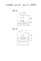
  • FIG. 1 shows a light I 0 entering a certain layer constituting the light-receiving layer of a light-receiving member, a reflected light R 1 from the upper interface 102 and a reflected light R 2 reflected from the lower interface 101.
  • the interference effect as shown in FIG. 1 occurs at each layer, and there ensues a synergistic deleterious influence through respective interferences as shown in FIG. 2. For this reason, the interference fringe corresponding to said interference fringe pattern appears on the visible image transferred and fixed on the transfer member to cause bad images.
  • the incident light I 0 is partly reflected from the surface of the light receiving layer 302 to become a reflected light R 1 , with the remainder progressing internally through the light receiving layer 302 to become a transmitted light I 1 .
  • the transmitted light I 1 is partly scattered on the surface of the substrate 301 to become scattered lights K 1 , K 2 , K 3 . . . K n , with the remainder being regularly reflected to become a reflected light R 2 , a part of which goes outside as an emitted light R 3 .
  • the reflected light R 1 and the emitted light R 3 which is an interferable component remain, it is not yet possible to extinguish the interference fringe pattern.
  • the reflected light R 2 from the first layer 402 the reflected light R 1 from the second layer 403 and the regularly reflected light R 3 from the surface of the substrate 401 are interfered with each other to form an interference fringe pattern depending on the respective layer thicknesses of the light-receiving member. Accordingly, in a light-receiving member of a multi-layer structure, it was impossible to completely prevent appearance of interference fringes by irregularly roughening the surface of the substrate 401.
  • the roughness will vary so much from lot to lot, and there is also nonuniformity in roughness even in the same lot, and therefore production control could be done with inconvenience.
  • relatively large projections with random distributions are frequently formed, hence causing local breakdown of the light-receiving layer during charging treatment.
  • An object of the present invention is to provide a novel light-receiving member sensitive to light, which has cancelled the drawbacks as described above.
  • Another object of the present invention is to provide a light-receiving member which is suitable for image formation by use of a coherent monochromatic light and also easy in production management.
  • Still another object of the present invention is to provide a light-receiving member which can cancel the interference fringe pattern appearing during image formation and appearance of speckles on reversal developing at the same time and completely.
  • Still another object of the prevent invention is to provide a light-receiving member which is high in dielectric strength and photosensitivity and excellent in electrophotographic characteristics.
  • Another object of the present invention is to provide a light-receiving member which can perform digital image recording utilizing electrophotography, above all digital image recording having a halftone information, clearly and at high resolution with high quality.
  • Still another object of the present invention is to provide a light-receiving member having high photosensitivity, high SN ratio characteristic and good electrical contact with a substrate.
  • Still another object of the present invention is to provide a light-receiving member comprising a substrate having a large number of protruding portions on a surface thereof, each of said protruding portions having at a predetermined cut position a sectional shape comprising a main projection and a subprojection, the main projection and the subprojection overlapping each other, and a light-receiving layer with a multi-layer structure having a first layer comprising an amorphous material containing silicon atoms and germanium atoms and a second layer comprising an amorphous material containing silicon atoms and exhibiting photoconductivity provided on said substrate successively from the substrate side.
  • FIG. 1 is a schematic illustration of interference fringe in general
  • FIG. 2 is a schematic illustration of interference fringe in the case of a multi-layer light-receiving member
  • FIG. 3 is a schematic illustration of interference fringe by scattered light
  • FIG. 4 is a schematic illustration of interference fringe by scattered light in the case of a multi-layer light-receiving member
  • FIG. 5 is a schematic illustration of interference fringe in the case where the interfaces of respective layers of a light-receiving member are parallel to each other;
  • FIGS. 6(A), (B), (C) and (D) are schematic illustrations of no appearance of interference fringe in the case of non-parallel interfaces between respective layers of a light-receiving member
  • FIGS. 7(A), (B) and (C) are schematic illustration of comparison of the reflected light intensity between the case of parallel interfaces and non-parallel interfaces between the respective layers of a light-receiving member;
  • FIG. 8 is a schematic illustration of no appearance of interference fringe in the case of non-parallel interfaces between respective layers
  • FIGS. 9(A), (B) and (C) are schematic illustrations of the surface condition of typical substrates
  • FIG. 10 is a schematic illustration of the layer constitution of a light-receiving member
  • FIGS. 11 through 19 are schematic illustrations of the distribution states of germanium atoms in the first layer
  • FIG. 20 is a schematic illustration of the vacuum deposition device for preparation of the light-receiving members employed in Examples
  • FIGS. 21(A), (B) and (C) are schematic illustrations of the surface states of the aluminum substrates employed in Examples.
  • FIGS. 22 to 25, FIGS. 36 to 42, FIGS. 52 to 62 and FIGS. 66 to 82 each is a schematic illustration of the change in gas flow rate of respective gases in Examples;
  • FIG. 26 is a schematic illustration of the image exposure device employed in Examples.
  • FIGS. 27 to 35 are illustrations for explanation of distribution states of the substance (C) in the layer region (PN);
  • FIGS. 43 to 51 are illustrations for explanation of distribution states of the atoms (OCN) in the layer region (OCN);
  • FIGS. 63 to 65 are illustrations of the surface states of the aluminum substrates employed in Examples.
  • FIG. 6 is a schematic illustration for explanation of the basic principle of the present invention.
  • a light-receiving layer of a multi-layer constitution is provided along the uneven slanted plane, with the thickness of the second layer 602 being continuously changed from d 5 to d 6 , as shown enlarged in a part of FIG. 6, and therefore the interface 603 and the interface 604 have respective gradients. Accordingly, the coherent light incident on this minute portion (short range region ) l [indicated schematically in FIG. 6(C), and its enlarged view shown in FIG. 6(A)] undergoes interference at said minute portion l to form a minute interference fringe pattern.
  • the layer thickness of the layer 602 may be macroscopically ununiform (d 7 ⁇ d 8 ), and therefore the incident light quantity becomes uniform all over the layer region (see FIG. 6(D)).
  • the interfaces between the respective layers at a minute portion function as a kind of slit, at which diffraction phenomenon will occur.
  • interference at respective layers appears as the effect of the product of interference due to difference in layer thickness and the interference due to difraction at the respective layer interfaces.
  • interference occurs as a synergetic effect of the respective layers and, according to the present invention, appearance of interference can further be prevented as the number of layers constituting the light-receiving layer is increased.
  • the interference fringe occurring within the minute portion cannot appear on the image, because the size of the minute portion is smaller than the spot size of the irradiated light, namely smaller than the resolution limit. Further, even if appeared on the image, there is no problem at all, since it is less than resolving ability of the eyes.
  • the slanted plane of unevenness should desirably be mirror finished in order to direct the reflected light assuredly in one direction.
  • the size l (one cycle of uneven shape) of the minute portion suitable for the present invention is l ⁇ L, wherein L is the spot size of the irradiation light.
  • the layer thickness difference (d 5 -d 6 ) at the minute portion l should desirably be as follows:
  • is the wavelength of the irradiation light and n is the refractive index of the second layer 602 (See FIG. 6).
  • the layer thicknesses of the respective layers are controlled so that at least two interfaces between layers may be in non-parallel relationship, and, provided that this condition is satisfied, any other pair of interfaces between layers may be in parallel relationship within said minute column.
  • the layers forming parallel interfaces should be formed to have uniform layer thicknesses so that the difference in layer thickness at any two positions may be not more than:
  • the plasma chemical vapor deposition method PCVD method
  • the optical CVD method the optical CVD method
  • thermal CVD method can be employed, because the layer thickness can accurately be controlled on the optical level thereby.
  • a substrate may be worked with a lathe by fixing a bite having a V-shaped cutting blade at a predetermined position on a cutting working machine such as milling machine, lathe, etc, and cut working accurately the substrate surface by, for example, moving regularly in a certain direction while rotating a cylindrical substrate according to a program previously designed as desired, thereby forming to a desired unevenness shape, pitch and depth.
  • the linear projection produced by the unevenness formed by such a cutting working has a spiral structure with the center axis of the cylindrical substrate as its center.
  • the spiral structure of the projection may be made into a multiple spiral structure such as double or triple structure or a crossed spiral structure.
  • a straight line structure along the center axis may also be introduced in addition to the spiral structure.
  • Each of the protruding portions formed on the surface of the substrate is preferred to have the same shape as the first order approximation at a predetermined section in order to make the working control easy.
  • each of the protruding portions has a sectional shape comprising a main projection (main peak) and a subprojection (subpeak), the main projection and the subprojection overlapping each other.
  • the above-mentioned protruding portions may be arranged regularly or periodically in order to enhance the effect of the invention.
  • the above-mentioned protruding portion for further enhancing the effect of the invention and enhancing adhesion between the light-receiving layer and the substrate, may preferably have multiple subprojections which may overlap each other.
  • the above-mentioned protruding portion may preferably be united in symmetrically [FIG. 9(A)] or asymmetrically [FIG. 9(B)] with the main projection at its center.
  • the respective dimensions of the unevenness provided on the substrate surface under managed condition are set so as to accomplish effectively the objects of the present invention in view of the following points.
  • the A-Si layer constituting the light-receiving layer is sensitive to the structure of the surface on which the layer formation is effected, and the layer quality will be changed greatly depending on the surface condition.
  • the pitch at the recessed portion on the substrate surface should preferably be 500 ⁇ m to 0.3 ⁇ m, more preferably 200 ⁇ m to 1 ⁇ m, most preferably 50 ⁇ m to 5 ⁇ m.
  • the maximum depth of the recessed portion should preferably be made 0.1 ⁇ m to 5 ⁇ m, more preferably 0.3 ⁇ m to 3 ⁇ m, most preferably 0.6 ⁇ m to 2 ⁇ m.
  • the gradient of the slanted plane at the recessed portion may preferably be 1° to 20°, more preferably 3° to 15°, most preferably 4° to 10°.
  • the maximum of the difference in the layer thickness based on such an uniformness in layer thickness of the respective layers formed on such a substrate should preferably be made 0.1 ⁇ m to 2 ⁇ m within the same pitch, more preferably 0.1 ⁇ m to 1.5 ⁇ m, most preferably 0.2 ⁇ m to 1 ⁇ m.
  • the light-receiving layer in the light-receiving member of the present invention has a multi-layer structure comprising a first layer constituted of an amorphous material containing silicon atoms and germanium atoms and a second layer constituted of an amorphous material containing silicon atoms and exhibiting photoconductivity provided on a substrate successively from the substrate side, and therefore can exhibit very excellent electrical, optical and photoconductive characteristics, dielectric strength as well as good use environmental characteristics.
  • the light-receiving member of the present invention is high in photosensitivity over the all visible light regions, particularly in photosensitivity to the light of longer wavelength region and is therefore excellent in matching to semiconductor laser and also rapid in light response.
  • FIG. 10 shows a schematic sectional view for illustration of the layer structure of an embodiment of the light-receiving member of the present invention.
  • the light-receiving member 1004 as shown in FIG. 10 has a light-receiving layer 1000 on a substrate for light-receiving member 1001, said light-receiving layer 1000 having a free surface 1005 on one end surface.
  • the light-receiving layer 1000 has a layer structure constituted of a first layer (G) 1002 comprising an amorphous material containing silicon atoms and germanium atoms and, if desired, hydrogen atoms (H) and/or halogen atoms (X) (hereinafter abbreviated as "A-SiGe(H,X)”) and a second layer (S) 1003 comprising A-Si containing, if desired, hydrogen atoms (H) and/or halogen atoms (X) (hereinafter abbreviated as A-Si(H,X)) and exhibiting photoconductivity laminated successively from the substrate 1001 side.
  • G first layer
  • S second layer
  • the germanium atoms contained in the first layer (G) 1002 may be contained so that the distribution state may be uniform within the first layer (G), or they can be contained continuously in the layer thickness direction in said first layer (G) 1002, being more enriched at the substrate 1001 side toward the side opposite to the side where said substrate 1001 is provided (the surface 1005 side of the light-receiving layer 1001).
  • the distribution state of the germanium atoms contained in the first layer (G) is ununiform in the layer thickness direction, it is desirable that the distribution state should be made uniform in the interplanar direction in parallel to the surface of the substrate.
  • the light-receiving member obtained in the second layer (S) provided on the first layer (G), no germanium atoms is contained and by forming a light-receiving layer to such a layer structure, the light-receiving member obtained can be excellent in photosensitivity to the light with wavelengths of all the regions from relatively shorter wavelength to relatively longer wavelength, including visible light region.
  • the germanium atoms in the first layer (G) are distributed continuously throughout the whole layer region while giving a change in distribution concentration C of the germanium atoms in the layer thickness direction which is decreased from the substrate toward the second layer (S), and therefore affinity between the first layer (G) and the second layer (S) is excellent.
  • affinity between the first layer (G) and the second layer (S) is excellent.
  • the respective amorphous materials constituting the first layer (G) and the second layer (S) have the common constituent of silicon atoms, and therefore chemical stability can sufficiently be ensured at the laminated interface.
  • FIGS. 11 through 19 show typical examples of distribution in the layer thickness direction of germanium atoms contained in the first layer region (G) of the light-receiving member in the present invention.
  • the abscissa indicates the content C of germanium atoms and the ordinate the layer thickness of the first layer (G), t B showing the position of the end surface of the first layer (G) on the substrate side and t T the position of the end surface of the first layer (G) on the side opposite to the substrate side. That is, layer formation of the first layer (G) containing germanium atoms proceeds from the t B side toward the t T side.
  • FIG. 11 there is shown a first typical embodiment of the depth profile of germanium atoms in the layer thickness direction contained in the first layer (G)
  • germanium atoms are contained in the first layer (G) formed, while the distribution concentration C of germanium atoms taking a constant value of C 1 , the concentration being gradually decreased from the concentration C 2 continuously from the position t 1 to the interface position t T .
  • the distribution concentration C of germanium atoms is made C 3 .
  • the distribution concentration C of germanium atoms contained is decreased gradually and continuously from the position t B to the position t T from the concentration C 4 until it becomes the concentration C 5 at the position t T .
  • the distribution concentration C of germanium atoms is made constant as C 6 at the position t B , gradually decreased continuously from the position t 2 to the position t T , and the concentration C is made substantially zero at the position t T (substantially zero herein means the content less than the detectable limit).
  • germanium atoms are decreased gradually and continuously from the position t B to the position t T from the concentration C 8 , until it is made substantially zero at the position t T .
  • the distribution concentration C of germanium atoms is constantly C 9 between the position t B and the position t 3 , and it is made C 10 at the position t T . Between the position t 3 and the position t T , the concentration C is decreased as a first order function from the position t 3 to the position t T .
  • the distribution concentration C takes a constant value of C 11 from the position t B to the position t 4 , and is decreased as a first order function from the concentration C 12 to the concentration C 13 from the position t 4 to the position t T .
  • the distribution concentration C of germanium atoms is decreased as a first order function from the concentration C 14 to zero from the position t B to the position t T .
  • FIG. 18 there is shown an embodiment, where the distribution concentration C of germanium atoms is decreased as a first order function from the concentration C 15 to C 16 from the position t B to t 5 and made constantly at the concentration C 16 between the position t 5 and t T .
  • the distribution concentration C of germanium atoms is at the concentration C 17 at the position t B , which concentration C 17 is initially decreased gradually and abruptly near the position t 6 to the position t 6 , until it is made the concentration C 18 at the position t 6 .
  • the concentration is initially decreased abruptly and thereafter gradually, until it is made the concentration C 19 at the position t 7 .
  • the concentration is decreased very gradually to the concentration C 20 at the position t 8 .
  • the concentration is decreased along the curve having a shape as shown in the Figure from the concentration C 20 to substantially zero.
  • the first layer (G) is provided desirably in a depth profile so as to have a portion enriched in distribution concentration C of germanium atoms on the substrate side and a portion depleted in distribution concentration C of germanium atoms considerably lower than that of the substrate side on the interface t T side.
  • the first layer (G) constituting the light-receiving member in the present invention is desired to have a localized region (A) containing germanium atoms at a relatively higher concentration on the substrate side as described above.
  • the localized region (A) may be desirably provided within 5 ⁇ from the interface position t B .
  • the above localized region (A) may be made to be identical with the whole of the layer region (L T ) on the interface position t B to the thickness of 5 ⁇ , or alternatively a part of the layer region (L T ).
  • the localized region (A) may preferably be formed according to such a layer formation that the maximum value Cmax of the concentrations of germanium atoms in a distribution in the layer thickness direction may preferably be 1000 atomic ppm or more, more preferably 5000 atomic ppm or more, most preferably 1 ⁇ 10 4 atomic ppm or more based on silicon atoms.
  • the layer region (G) containing germanium atoms is formed so that the maximum value Cmax of the distribution concentration C may exist within a layer thickness of 5 ⁇ from the substrate side (the layer region within 5 ⁇ thickness from t B ).
  • the content of germanium atoms in the first layer (G), which may suitably be determined as desired so as to acheive effectively the objects of the present invention, may preferably be 1 to 9.5 ⁇ 10 5 atomic ppm, more preferably 100 to 8 ⁇ 10 5 atomic ppm, most preferably 500 to 7 ⁇ 10 5 atomic ppm.
  • the layer thickness of the first layer (G) and the thickness of the second layer (S) are one of the important factors for accomplishing effectively the objects of the present invention, and therefore sufficient care should desirably be paid in designing of the light-receiving member so that desirable characteristics may be imparted to the light-receiving member formed.
  • the layer thickness T B of the first layer (G) may preferably be 30 ⁇ to 50 ⁇ , more preferably 40 ⁇ to 40 ⁇ , most preferably 50 ⁇ to 30 ⁇ .
  • the layer thickness T of the second layer (S) may be preferably 0.5 to 90 ⁇ , more preferably 1 to 80 ⁇ , most preferably 2 to 50 ⁇ .
  • the sum of the above layer thicknesses T and T B may be suitably determined as desired in designing of the layers of the light-receiving member, based on the mutual organic relationship between the characteristics required for both layer regions and the characteristics required for the whole light-receiving layer.
  • the numerical range for the above (T B +T) may generally be from 1 to 100 ⁇ , preferably 1 to 80 ⁇ , most preferably 2 to 50 ⁇ .
  • the values of T B and T should preferably be determined so that the relation T B /T ⁇ 0.9, most preferably, T B /T ⁇ 0.8, may be satisfied.
  • the layer thickness T B should desirably be made considerably thinner, preferably 30 ⁇ or less, more preferably 25 ⁇ or less, most preferably 20 ⁇ or less.
  • halogen atoms (X) which may optionally be incorporated in the first layer (G) and the second layer (S) constituting the light-receiving layer, are fluorine, chlorine, bormine and iodine, particularly preferably fluorine and chlorine.
  • formation of the first layer (G) constituted of A-SiGe(H,X) may be conducted according to the vacuum deposition method utilizing discharging phenomenon, such as glow discharge method, sputtering method or ion-plating method.
  • the basic procedure comprises introducing a starting gas for Si supply capable of supplying silicon atoms (Si), a starting gas for Ge supply capable of supplying germanium atoms (Ge) optionally together with a starting gas for introduction of hydrogen atoms (H) and/or a starting gas for introduction of halogen atoms (X) into a deposition chamber which can be internally brought to a reduced pressure, and exciting glow discharge in said deposition chamber, thereby effecting layer formation on the surface of a substrate placed at a predetermined position while controlling the depth profile of germanium atoms according to a desired rate of change curve to form a layer constituent of A-SiGe (H,X).
  • a gas for introduction of hydrogen atoms (H) and/or a gas for introduction of halogen atoms (X) may be introduced, if desired, into a deposition chamber for sputtering.
  • the starting gas for supplying Si to be used in the present invention may include gaseous or gasifiable hydrogenated silicons (silanes) such as SiH 4 , Si 2 H 6 , Si 3 H 8 , Si 4 H 10 and others as effective materials.
  • SiH 4 and Si 2 H 6 are preferred because of easiness in handling during layer formation and high efficiency for supplying Si.
  • germanium such as GeH 4 , Ge 2 H 6 , Ge 3 H 8 , Ge 4 H 10 , Ge 5 H 12 , Ge 6 H 14 , Ge 7 H 16 , Ge 8 H 18 , Ge 9 H 20 , etc.
  • GeH 4 , Ge 2 H 6 and Ge 3 H 8 are preferred because of easiness in handling during layer formation and high efficiency for supplying Ge.
  • Effective starting gases for introduction of halogen atoms to be used in the present invention may include a large number of halogenic compounds, as exemplified preferably by halogenic gases, halides, interhalogen compounds, or gaseous or gasifiable halogenic compounds such as silane derivatives substituted with halogens.
  • gaseous or gasifiable hydrogenated silicon compounds containing halogen atoms constituted of silicon atoms and halogen atoms as constituent elements as effective ones in the present invention.
  • halogen compounds preferably used in the present invention may include halogen gases such as of fluorine, chlorine, bromine or iodine, interhalogen compounds such as BrF, ClF, ClF 3 , BrF 5 , BrF 3 , IF 3 , IF 7 , ICl, IBr, etc.
  • halogen gases such as of fluorine, chlorine, bromine or iodine
  • interhalogen compounds such as BrF, ClF, ClF 3 , BrF 5 , BrF 3 , IF 3 , IF 7 , ICl, IBr, etc.
  • silicon compounds containing halogen atoms namely so called silane derivatives substituted with halogens
  • silicon halides such as SiF 4 , Si 2 F 6 , SiCl 4 , SiBr 4 and the like.
  • the light-receiving member of the present invention is formed according to the glow discharge method by employment of such a silicon compound containing halogen atoms, it is possible to form the first layer (G) constituted of A-SiGe containing halogen atoms on a desired substrate without use of a hydrogenated silicon gas as the starting gas capable of supplying Si together with the starting gas for Ge supply.
  • the basic procedure comprises introducing, for example, a silicon halide as the starting gas for Si supply, a hydrogenated germanium as the starting gas for Ge supply and a gas such as Ar, H 2 , He, etc. at a predetermined mixing ratio into the deposition chamber for formation of the first layer (G) and exciting glow discharge to form a plasma atmosphere of these gases, whereby the first layer (G) can be formed on a desired substrate.
  • a silicon halide as the starting gas for Si supply
  • a hydrogenated germanium as the starting gas for Ge supply
  • a gas such as Ar, H 2 , He, etc.
  • each gas is not restricted to a single species, but multiple species may be available at any desired ratio.
  • the first layer (G) comprising A-SiGe(H,X) according to the reactive sputtering method or the ion plating method
  • the sputtering method two sheets of a target of Si and a target of Ge or a target of Si and Ge is employed and subjected to sputtering in a desired gas plasma atmosphere.
  • a vaporizing source such as a polycrystalline silicon or a single crystalline silicon and a polycrystalline germanium or a single crystalline germanium may be placed as vaporizing source in an evaporating boat, and the vaporizing source is heated by the resistance heating method or the electron beam method (EB method) to be vaporized, and the flying vaporized product is permitted to pass through a desired gas plasma atmosphere.
  • EB method electron beam method
  • introduction of halogen atoms into the layer formed may be performed by introducing the gas of the above halogen compound or the above silicon compound containing halogen atoms into a deposition chamber and forming a plasma atmosphere of said gas.
  • a starting gas for introduction of hydrogen atoms for example, H 2 or gases such as silanes and/or hydrogenated germanium as mentioned above, may be introduced into a deposition chamber for sputtering, followed by formation of the plasma atmosphere of said gases.
  • the starting gas for introduction of halogen atoms the halides or halo-containing silicon compounds as mentioned above can effectively be used. Otherwise, it is also possible to use effectively as the starting material for formation of the first layer (G) gaseous or gasifiable substances, including halides containing hydrogen atom as one of the constituents, e.g.
  • hydrogen halide such as HF, HCl, HBr, HI, etc.
  • halo-substituted hydrogenated silicon such as SiH 2 F 2 , SiH 2 I 2 , SiH 2 Cl 2 , SiHCl 3 , SiH 2 Br 2 , SiHBr 3 , etc.
  • hydrogenated germanium halides such as GeHF 3 , GeH 2 F 2 , GeH 3 F, GeHCl 3 , GeH 2 Cl 2 , GeH 3 Cl, GeHBr 3 , GeH 2 Br 2 , GeH 3 Br, GeHI 3 , GeH 2 I 2 , GeH 3 I, etc.
  • germanium halides such as GeF 4 , GeCl 4 , GeBr 4 , GeI 4 , GeF 2 , GeCl 2 , GeBr 2 , GeI 2 , etc.
  • halides containing halogen atoms can preferably be used as the starting material for introduction of halogens, because hydrogen atoms, which are very effective for controlling electrical or photoelectric characteristics, can be introduced into the layer simultaneously with introduction of halogen atoms during formation of the first layer (G).
  • H 2 or a hydrogenated silicon such as SiH 4 , Si 2 H 6 , Si 3 H 8 , Si 4 H 10 , etc. together with germanium or a germanium compound for supplying Ge
  • a hydrogenated germanium such as GeH 4 , Ge 2 H 6 , Ge 3 H 8 , Ge 4 H 10 , Ge 5 H 12 , Ge 6 H 14 , Ge 7 H 16 , Ge 8 H 18 , Ge 9 H 20 , etc. together with silicon or a silicon compound for supplying Si can be permitted to co-exist in a deposition chamber, followed by excitation of discharging.
  • the amount of hydrogen atoms (H) or the amount of halogen atoms (X) or the sum of the amounts of hydrogen atoms and halogen atoms (H+X) to be contained in the first layer (G) constituting the light-receiving layer to be formed should preferably be 0.01 to 40 atomic %, more preferably 0.05 to 30 atomic %, most preferably 0.1 to 25 atomic %.
  • the substrate temperature and/or the amount of the starting materials used for incorporation of hydrogen atoms (H) or halogen atoms (X) to be introduced into the deposition device system, discharging power, etc. may be controlled.
  • the starting materials (I) for formation of the first layer (G), from which the starting materials for the starting gas for supplying Ge are omitted, are used as the starting materials (II) for formation of the second layer (S), and layer formation can be effected following the same procedure and conditions as in formation of the first layer (G).
  • formation of the second layer region (S) constituted of a-Si(H,X) may be carried out according to the vacuum deposition method utilizing discharging phenomenon such as the glow discharge method, the sputtering method or the ion-plating method.
  • the basic procedure comprises introducing a starting gas for Si supply capable of supplying silicon atoms (Si) as described above, optionally together with starting gases for introduction of hydrogen atoms (H) and/or halogen atoms (X), into a deposition chamber which can be brought internally to a reduced pressure and exciting glow discharge in said deposition chamber, thereby forming a layer comprising A-Si(H,X) on a desired substrate placed at a predetermined position.
  • gases for introduction of hydrogen atoms (H) and/or halogen atoms (X) may be introduced into a deposition chamber when effecting sputtering of a target constituted of Si in an inert gas such as Ar, He, etc. or a gas mixture based on these gases.
  • the amount of hydrogen atoms (H) or the amount of halogen atoms (X) or the sum of the amounts of hydrogen atoms and halogen atoms (H+X) to be contained in the second layer (S) constituting the light-receiving layer to be formed should preferably be 1 to 40 atomic %, more preferably 5 to 30 atomic %, most preferably 5 to 25 atomic %.
  • the light-receiving member 1004 by incorporating a substance (C) for controlling conductivity in at least the first layer (G) 1002 and/or the second layer (S) 1003, desired conductivity characteristics can be given to the layer containing said substance (C).
  • the substance (C) for controlling conductivity may be contained throughout the whole layer region in the layer containing the substance (C) or contained locally in a part of the layer region of the layer containing the substance (C).
  • the distribution state of said substance (C) in the layer thickness direction may be either uniform or nonuniform, but desirably be made uniform within the plane in parallel to the substrate surface.
  • the distribution state of the substance (C) is nonuniform in the layer thickness direction, and when the substance (C) is to be incorporated in the whole layer region of the first layer (G), said substance (C) is contained in the first layer (G) so that it may be more enriched on the substrate side of the first layer (G).
  • the layer region (PN) in which the substance (C) is to be contained is provided as an end portion layer region of the first layer (G), which is to be determined case by case suitably as desired depending on.
  • the substance (C) when the above substance (C) is to be incorporated in the second layer (S), it is desirable to incorporate the substance (C) in the layer region including at least the contacted interface with the first layer (G).
  • the layer region containing the substance (C) in the first layer (G) and the layer region containing the substance (C) in the second layer (S) may contact each other.
  • the above substance (C) contained in the first layer (G) may be either the same as or different from that contained in the second layer (S), and their contents may be either the same or different.
  • a substance (C) for controlling conductivity in at least the first layer (G) and/or the second layer (S) constituting the light-receiving layer, conductivity of the layer region containing the substance (C) [which may be either a part or the whole of the layer region of the first layer (G) and/or the second layer (S)] can be controlled as desired.
  • a substance (C) for controlling conductivity characteristics there may be mentioned so called impurities in the field of semiconductors.
  • p-type impurities giving p-type condutivity characteristics and n-type impurities and/or giving n-type conductivity characteristics to A-Si(H,X) and/or A-SiGe(H,X) constituting the light receiving layer to be formed.
  • Group III atoms such as B (boron), Al(aluminum), Ga(gallium), In(indium), Tl(thallium), etc., particularly preferably B and Ga.
  • n-type impurities there may be included the atoms belonging to the group V of the periodic table, such as P (phosphorus), As (arsenic), Sb (antimony), Bi (bismuth), etc., particularly preferably P and As.
  • the content of the substance (C) for controlling conductivity in the layer region (PN) may be suitably be determined depending on the conductivity required for said layer region (PN), or when said layer region (PN) is provided in direct contact with the substrate, the organic relationships such as relation with the characteristics at the contacted interface with the substrate, etc.
  • the content of the substance (C) for controlling conductivity is determined suitably with due considerations of the relationships with characteristics of other layer regions provided in direct contact with said layer region or the characteristics at the contacted interface with said other layer regions.
  • the content of the substance (C) for controlling conductivity contained in the layer region (PN) should preferably be 0.01 to 5 ⁇ 10 4 atomic ppm, more preferably 0.5 to 1 ⁇ 10 4 atomic ppm, most preferably 1 to 5 ⁇ 10 3 atomic ppm.
  • the content of said substance (C) in the layer region (PN) preferably 30 atomic ppm or more, more preferably 50 atomic ppm or more, most preferably 100 atomic ppm or more, for example, in the case when said substance (C) to be incorporated is a p-type impurity as mentioned above, migration of electrons injected from the substrate side into the light-receiving layer can be effectively inhibited when the free surface of the light-receiving layer is subjected to the charging treatment to ⁇ polarity.
  • the substance to be incorporated is a n-type impurity
  • migration of positive holes injected from the substrate side into the light-receiving layer may be effectively inhibited when the free surface of the light-receiving layer is subjected to the charging treatment to ⁇ polarity.
  • the layer region (Z) at the portion excluding the above layer region (PN) under the basic constitution of the present invention as described above may contain a substance for controlling conductivity of the other polarity, or a substance for controlling conductivity having characteristics of the same polarity may be contained therein in an amount by far smaller than that practically contained in the layer region (PN).
  • the content of the substance (C) for controlling conductivity contained in the above layer region (Z) can be determined adequately as desired depending on the polarity or the content of the substance contained in the layer region (PN), but it is preferably 0.001 to 1000 atomic ppm, more preferably 0.05 to 500 atomic ppm, most preferably 0.1 to 200 atomic ppm.
  • the content in the layer region (Z) should preferably be 30 atomic ppm or less.
  • a layer containing the aforesaid p-type impurity and a layer region containing the aforesaid n-type impurity are provided in the light-receiving layer in direct contact with each other to form the so called p-n junction, whereby a depletion layer can be provided.
  • FIGS. 27 through 35 show typical examples of the depth profiles in the layer thickness direction of the substance (C) contained in the layer region (PN) in the light-receiving layer of the present invention.
  • representations of layer thickness and concentration are shown in rather exaggerated forms for illustrative purpose, since the difference between respective Figures will be indistinct if represented by the real values as such, and it should be understood that these Figures are schematic in nature.
  • the values of ti (1 ⁇ i ⁇ 9) or Ci (1 ⁇ i ⁇ 17) chosen so as to obtain desired distribution concentration lines, or values obtained by multiplying the distribution curve as a whole with an appropriate coefficient should be used.
  • the abscissa shows the distribution concentration C of the substance (C), and the ordinate the layer thickness of the layer region (PN), t B indicating the position of the end surface on the substrate side of the layer region (G) and t T the position of the end surface on the side opposite to the substrate side.
  • layer formation of the layer region (PN) containing the substance (C) proceeds from the t B side toward the t T side.
  • FIG. 27 shows a first typical example of the depth profile of the substance (C) in the layer thickness direction contained in the layer region (PN).
  • the substance (C) is contained in the layer region (PN) formed while the distribution concentration C of the substance (C) taking a constant value of C 1 , and the concentration is gradually decreased from the concentration C 2 continuously from the position t 1 to the interface position t T .
  • the distribution concentration C of the substance (C) is made substantially zero (here substantially zero means the case of less than detectable limit).
  • the distribution concentration C of the substance (C) contained is decreased from the position t B to the position t T gradually and continuously from the concentration C 3 to the concentration C 4 at t T .
  • the distribution concentration C of the substance (C) is made constantly at C 5 , while between the position t 2 and the position t T , it is gradually and continuously decreased, until the distribution concentration is made substantially zero at the position t T .
  • the distribution concentration C of the substance (C) is first decreased continuously and gradually from the concentration C 6 from the position t B to the position t 3 , from where it is abruptly decreased to substantially zero at the position t T .
  • the distribution concentration of the substance (C) is constantly C 7 between the position t B and the position t T , and the distribution concentration is made zero at the position t T . Between the t 4 and the position t T , the distribution concentration C is decreased as a first order function from the position t 4 to the position t T .
  • the distribution concentration C takes a constant value of C 8 from the position t B to the position t 5 , while it was decreased as a first order function from the concentration C 9 to the concentration C 10 from the position t 5 to the position t T .
  • the distribution concentration C of the substance (C) is decreased continuously as a first order function from the concentration C 11 to zero.
  • FIG. 34 there is shown an embodiment, in which, from the position t B to the position t 6 , the distribution concentration C of the substance C is decreased as a first order function from the concentration C 12 to the concentration C 13 , and the concentration is made a constant value of C 13 between the position t 6 and the position t T .
  • the distribution concentration C of the substance (C) is C 14 at the position t B , which is gradually decreased initially from C 14 and then abruptly near the position t 7 , where it is made C 15 at the position t 7 .
  • the concentration is initially abruptly decreased and then moderately gradually, until it becomes C 16 at the position t 8 , and between the position t 8 and the position t 9 , the concentration is gradually decreased to reach C 17 at the position t 9 .
  • the concentration is decreased from C 17 , following the curve with a shape as shown in Figure, to substantially zero.
  • a depth profile of the substance (C) should be provided in the layer region (PN) so as to have a portion with relatively higher distribution concentration C of the substance (C) on the substrate side, while having a portion on the interface t T side where said distribution concentration is made considerably lower as compared with the substrate side.
  • the layer region (PN) constituting the light-receiving member in the present invention is desired to have a localized region (B) containing the substance (C) preferably at a relatively higher concentration on the substrate side as described above.
  • the localized region (B) as explained in terms of the symbols shown in FIGS. 27 through 35, may be desirably provided within 5 ⁇ from the interface position t B .
  • the above localized region (B) may be made to be identical with the whole of the layer region (L) from the interface position t B to the thickness of 5 ⁇ , or alternatively a part of the layer region (L).
  • the localized region (B) may suitably be made a part or the whole of the layer region (L).
  • a starting material for introduction of the group III atoms or a starting material for introduction of the group V atoms may be introduced under gaseous state into a deposition chamber together with other starting materials for formation of the respective layers during layer formation.
  • the starting material which can be used for introduction of the group III atoms it is desirable to use those which are gaseous at room temperature under atmospheric pressure or can readily be gasified under layer forming conditions.
  • Typical examples of such starting materials for introduction of the group III atoms there may be included as the compounds for introduction of boron atoms boron hydrides such as B 2 H 6 , B 4 H 10 , B 5 H 9 , B 5 H 11 , B 6 H 10 , B 6 H 12 , B 6 H 14 , etc. and boron halides such as BF 3 , BCl 3 , BBr 3 , etc.
  • boron halides such as BF 3 , BCl 3 , BBr 3 , etc.
  • the starting materials which can effectively be used in the present invention for introduction of the group V atoms may include, for introduction of phosphorus atoms, phosphorus hydrides such as PH 3 , P 2 H 4 , etc., phosphorus halides such as PH 4 I, PF 3 , PF 5 , PCl 3 , PCl 5 , PBr 3 , PBr 5 , PI 3 and the like.
  • At least one kind of atoms selected from oxygen atoms, carbon atoms and nitrogen atoms can be contained in the light-receiving layer in either uniform or ununiform distribution state in the layer thickness direction.
  • Such atoms (OCN) to be contained in the light-receiving layer may be contained therein throughout the whole layer region of the light-receiving layer or localized by being contained in a part of the layer region of the light-receiving layer.
  • the distribution concentration C (OCN) of the atoms (OCN) should desirably be uniform within the plane parallel to the surface of the substrate.
  • the layer region (OCN) where atoms (OCN) are contained is provided so as to occupy the whole layer region of the light-receiving layer when it is primarily intended to improve photosensitivity and dark resistance, while it is provided so as to occupy the end portion layer region on the substrate side of the light-receving layer when it is primarily intended to strengthen adhesion between the substrate and the light-receiving layer.
  • the content of atoms (OCN) contained in the layer region (OCN) should desirably be made relatively smaller in order to maintain high photosensitivity, while in the latter case relatively larger in order to ensure reinforcement of adhesion to the substrate.
  • the content of the atoms (OCN) to be contained in the layer region (OCN) provided in the light-receiving layer can be selected suitably in organic relationship with the characteristics required for the layer region (OCN) itself, or with the characteristic at the contacted interface with the substrate when the said layer region (OCN) is provided in direct contact with the substrate, etc.
  • the content of the atoms (OCN) may suitably be selected with due considerations about the characteristics of said other layer regions or the characteristics at the contacted interface with said other layer regions.
  • the amount of the atoms (OCN) contained in the layer region (OCN) may be determined as desired depending on the characteristics required for the light-receiving member to be formed, but it may preferably be 0.001 to 50 atomic %, more preferably 0.002 to 40 atomic %, most preferably 0.003 to 30 atomic %.
  • the layer region (OCN) occupies the whole region of the light-receiving layer or, although not occupying the whole region, the proportion of the layer thickness T O of the layer region (OCN) occupied in the layer thickness T of the light-receiving layer is sufficiently large, the upper limit of the content of the atoms (OCN) contained in the layer region (OCN) should desirably be made sufficiently smaller than the value as specified above.
  • the upper limit of the atoms (OCN) contained in the layer region (OCN) should desirably be made 30 atomic % or less, more preferably 20 atomic % or less, most preferably 10 atomic % or less.
  • the atoms (OCN) should be contained in at least the above first layer to be provided directly on the substrate.
  • OCN atoms
  • OCN oxygen atoms
  • oxygen atoms may be contained in the first layer, nitrogen atoms in the second layer, or alternatively oxygen atoms and nitrogen atoms may be permitted to be co-present in the same layer region.
  • FIGS. 43 through 51 show typical examples of ununiform depth profiles in the layer thickness direction of the atoms (OCN) contained in the layer region (OCN) in the light-receiving member of the present invention.
  • the abscissa indicates the distribution concentration C of the atoms (OCN), and the ordinate the layer thickness of the layer region (OCN), t B showing the position of the end surface of the layer region on the substrate side, while t T shows the position of the end face of the layer region (OCN) opposite to the substrate side.
  • layer formation of the layer region (OCN) containing the atoms (OCN) proceeds from the t B side toward the t T side.
  • FIG. 43 shows a first typical embodiment of the depth profile in the layer thickness direction of the atoms (OCN) contained in the layer region (OCN).
  • the distribution concentration C of the atoms (OCN) contained is reduced gradually continuously from the concentration C 4 from the position t B to the position t T , at which it becomes the concentration C 5 .
  • the distribution concentration of the atoms (OCN) is made constantly at C 6 , reduced gradually continuously from the concentration C 7 between the position t 2 and the position t T , until at the position t T , the distribution concentration C is made substantially zero (here substantially zero means the case of less than the detectable level).
  • the distribution concentration C of the atoms (OCN) is reduced gradually continuously from the concentration C 8 from the position t B up to the position t T , to be made substantially zero at the position t T .
  • the distribution concentration C of the atoms (OCN) is made constantly C 9 between the position t B and the position t 3 , and it is made the concentration C 10 at the position t T . Between the position t 3 and the position t T , the distribution concentration C is reduced from the concentration C 9 to substantially zero as a first order function from the position t 3 to the position t T .
  • the distribution concentration C takes a constant value of C 11 , while the distribution state is changed to a first order function in which the concentration is decreased from the concentration C 12 to the concentration C 13 from the position t 4 to the position t T , and the concentration C is made substantially zero at the position t T .
  • the distribution concentration C of the atoms (OCN) is reduced as a first order function from the concentration C 14 to substantially zero.
  • FIG. 50 there is shown an embodiment, wherein from the position t B to the position t 5 , the distribution concentration of the atoms (OCN) is reduced approximately as a first order function from the concentration C 15 to C 16 , and it is made constantly C 16 between the position t 5 and the position t T .
  • OCN distribution concentration of the atoms
  • the distribution concentration C of the atoms (OCN) is C 17 at the position t B , and, toward the position t 6 , this C 17 is initially reduced gradually and then abruptly reduced near the position t 6 , until it is made the concentration C 18 at the position t 6 .
  • the concentration is initially reduced abruptly and thereafter gently gradually reduced to become C 19 at the position t 7 , and between the position t 7 and the position t 8 , it is reduced very gradually to become C 20 at the position t 8 .
  • the concentration is reduced from the concentration C 20 to substantially zero along a curve with a shape as shown in the Figure.
  • the atoms (OCN) As described above about some typical examples of depth profiles in the layer thickness direction of the atoms (OCN) contained in the layer region (OCN) by referring to FIGS. 43 through 51, it is desirable in the present invention that, when the atoms (OCN) are to be contained ununiformly in the layer region (OCN), the atoms (OCN) should be distributed in the layer region (OCN) with higher concentration on the substrate side, while having a portion considerably depleted in concentration on the interface t T side as compared with the substrate side.
  • the layer region (OCN) containing atoms (OCN) should desirably be provided so as to have a localized region (B) containing the atoms (OCN) at a relatively higher concentration on the substrate side as described above, and in this case, adhesion between the substrate and the light-receiving layer can be further improved.
  • the above localized region (B) should desirably be provided within 5 ⁇ from the interface position t B , as explained in terms of the symbols indicated in FIGS. 43 through 51.
  • the above localized region (B) may be made the whole of the layer region (L T ) from the interface position t B to 5 ⁇ thickness or a part of the layer region (L T ).
  • the localized region (B) is made a part or the whole of the layer region (L T ).
  • the localized region (B) should preferably be formed to have a depth profile in the layer thickness direction such that the maximum value Cmax of the distribution concentration of the atoms (OCN) may preferably be 500 atomic ppm or more, more preferably 800 atomic ppm or more, most preferably 1000 atomic ppm or more.
  • the layer region (OCN) containing the atoms (OCN) should preferably be formed so that the maximum value Cmax of the distribution concentration C may exist within 5 ⁇ layer thickness from the substrate side (in the layer region with 5 ⁇ thickness from t B ).
  • the depth profile of the atoms (OCN) should desirably be formed so that the refractive index may be changed moderately at the interface between the layer region (OCN) and other layer regions.
  • the distribution concentration C of the atoms (OCN) in the layer region (OCN) should be changed along a line which is changed continuously and moderately, in order to give smooth refractive index change.
  • the atoms (OCN) should be contained in the layer region (OCN) so that the depth profiles as shown, for example, in FIGS. 43 through 46, FIG. 49 and FIG. 51 may be assumed.
  • a starting material for introduction of the atoms (OCN) may be used together with the starting material for formation of the light-receiving layer during formation of the light-receiving layer and incorporated in the layer formed while controlling its amount.
  • a starting material for introduction of the atoms (OCN) is added to the material selected as desired from the starting materials for formation of the light-receiving layer as described above.
  • a starting material for introduction of the atoms (OCN) there may be employed most of gaseous or gasified gasifiable substances containing at least the atoms (OCN) as the constituent atoms.
  • the starting material for introduction of the atoms there may also be employed solid starting materials such as SiO 2 , Si 3 N 4 and carbon black in addition to those gasifiable as enumerated for the glow discharge method. These can be used in the form of a target for sputtering together with the target of Si, etc.
  • formation of the layer region (OCN) having a desired depth profile in the direction of layer thickness formed by varying the distribution concentration C of the atoms (OCN) contained in said layer region (OCN) may be conducted in the case of glow discharge by introducing a starting gas for introduction of the atoms (OCN) the distribution concentration C of which is to be varied into a deposition chamber, while varying suitably its gas flow rate according to a desired change rate curve.
  • the opening of a certain needle valve provided in the course of the gas flow channel system may be gradually varied.
  • the rate of variation is not necessarily required to be linear, but the flow rate may be controlled according to a variation rate curve previously designed by means of, for example, a microcomputer to give a desired content curve.
  • the layer region (OCN) is formed according to the sputtering method
  • formation of a desired depth profile of the atoms (OCN) in the layer thickness direction by varying the distribution concentration C of the atoms (OCN) may be performed first similarly as in the case of the glow discharge method by employing a starting material for introduction of the atoms (OCN) under gaseous state and varying suitably as desired the gas flow rate of said gas when introduced into the deposition chamber.
  • formation of such a depth profile can also be achieved by previously changing the composition of a target for sputtering. For example, when a target comprising a mixture of Si and SiO 2 is to be used, the mixing ratio of Si to SiO 2 may be varied in the direction of layer thickness of the target.
  • the substrate to be used in the present invention may be either electroconductive or insulating.
  • the electroconductive substrate there may be mentioned metals such as NiCr, stainless steel, Al, Cr, Mo, Au, Nb, Ta, V, Ti, Pt, Pd etc. or alloys thereof.
  • insulating substrates there may conventionally be used films or sheets of synthetic resins, including polyester, polyethylene, polycarbonate, cellulose acetate, polypropylene, polyvinyl chloride, polyvinylidene chloride, polystyrene, polyamide, etc., glasses, ceramics, papers and so on. At least one side surface of these substrates is preferably subjected to treatment for imparting electroconductivity, and it is desirable to provide other layers on the side at which said electroconductive treatment has been applied.
  • electroconductive treatment of a glass can be effected by providing a thin film of NiCr, Al, Cr, Mo, Au, Ir, Nb, Ta, V, Ti, Pt, Pd, In 2 O 3 , SnO 2 , ITO (In 2 O 3 +SnO 2 ) thereon.
  • a synthetic resin film such as polyester film can be subjected to the electroconductive treatment on its surface by vacuum vapor deposition, electron-beam deposition or sputtering of a metal such as NiCr, Al, Ag, Pb, Zn, Ni, Au, Cr, Mo, Ir, Nb, Ta, V, Ti, Pt, etc. or by laminating treatment with said metal, thereby imparting electroconductivity to the surface.
  • the substrate may be shaped in any form such as cylinders, belts, plates or others, and its form may be determined as desired.
  • the light-receiving member 1004 in FIG. 10 when it is to be used as the light-receiving member for electrophotography, it may desirably be formed into an endless belt or a cylinder for use in continuous high speed copying.
  • the substrate may have a thickness, which is conveniently determined so that the light-receiving member as desired may be formed.
  • the substrate is made as thin as possible, so far as the function of a support can be exhibited.
  • the thickness is generally 10 ⁇ or more from the points of fabrication and handling of the substrate as well as its mechanical strength.
  • FIG. 20 shows one example of a device for producing a light-receiving member.
  • SiH 4 germanium oxide
  • GeH 4 germanium oxide
  • NO nitrogen
  • B 2 H 6 B 2 H 6 /H 2
  • 2006 is a bomb containing H 2 gas (purity: 99.999%).
  • the main valve 2034 is first opened to evacuate the reaction chamber 2001 and the gas pipelines.
  • the auxiliary valves 2032, 2033 and the outflow valves 2017 to 2021 are closed.
  • SiH 4 gas from the gas bomb 2002, GeH 4 gas from the gas bomb 2003, NO gas from the gas bomb 2004, B 2 H 6 /H 2 gas from the gas bomb 2005 and H 2 gas from the gas bomb 2006 are permitted to flow into the mass-flow controllers 2007, 2008, 2009, 2010 and 2011, respectively, by opening the valves 2022, 2023, 2024, 2025 and 2026 and controlling the pressures at the output pressure gauges 2027, 2028, 2029 2030 and 2031 to 1 Kg/cm 2 and opening gradually the inflow valves 2012, 2013, 2014, 2015 and 2016, respectively.
  • the outflow valves 2017, 2018, 2019, 2020 and 2021 and the auxiliary valves 2032 and 2033 were gradually opened to permit respective gases to flow into the reaction chamber 2001.
  • the outflow valves 2017, 2018, 2019, 2020 and 2021 are controlled so that the flow rate ratio of SiH 4 gas, GeH 4 gas, B 2 H 6 /H 2 gas, NO gas and H 2 may have a desired value and opening of the main valve 2034 is also controlled while watching the reading on the vacuum indicator 2036 so that the pressure in the reaction chamber 2001 may reach a desired value. And, after confirming that the temperature of the substrate 2037 is set at 50° to 400° C.
  • the power source 2040 is set at a desired power to excite glow discharge in the reaction chamber 2001, simultaneously with controlling of the distributed concentrations of germanium atoms and boron atoms to be contained in the layer formed by carrying out the operation to change gradually the openings of the valves 2018, 2020 by the manual method or by means of an externally driven motor, etc. thereby changing the flow rates of GeH 4 gas and B 2 H 6 gas according to previously designed change rate curves.
  • the first layer (G) is formed on the substrate 2037 to a desired thickness.
  • the second layer (S) containing substantially no germanium atom can be formed on the first layer (G) by maintaining glow discharge according to the same conditions and procedure as those in formation of the first layer (G) except for closing completely the outflow valve 2018 and changing, if desired, the discharging conditions.
  • oxygen atoms or boron atoms may be contained or not, or oxygen atoms or boron atoms may be contained only in a part of the layer region of the respective layers.
  • layer formation may be conducted by replacing NO gas in the gas bomb 2004 with NH 3 or CH 4 . Also, when the kinds of the gases employed are desired to be increased, bombs of desirable gases may be provided additionally before carrying out layer formation similarly.
  • the surface condition of a light-receiving member for electrophotography thus prepared was as shown in FIG. 21(C).
  • the light-receiving member for electrophotography as prepared above was subjected to image exposure by means of a device as shown in FIG. 26 (wavelength of laser beam: 780 nm, spot diameter 80 ⁇ m), followed by developing and transfer to obtain an image.
  • the image was free from any interference fringe pattern observed and proved to be satisfactory for practical application.
  • the images obtained were free from any interference fringe pattern, having practically satisfactory characteristics.
  • the images obtained were free from any interference fringe pattern, having practically satisfactory characteristics.
  • an aluminum substrate (length (L): 357 mm, outer diameter (r): 80 mm) was worked as shown in FIG. 21(B).
  • a light-receiving member for electrophotography of A-Si:H type was prepared following various procedures using the deposition device in FIG. 20 under the conditions as shown in Table 1B.
  • the A-Si:Ge:H layer as the first layer was formed while controlling the flow rate of GeH 4 and SiH 4 as shown in FIG. 22 by operating mass flow controllers 2007 and 2008 for GeH 4 and SiH 4 , respectively, using a computer (HP9845B).
  • the light-receiving member for electrophotography as prepared above was subjected to image exposure by means of a device as shown in FIG. 26 (wavelength of laser beam: 780 nm, spot diameter 80 ⁇ m), followed by developing and transfer to obtain an image.
  • the image was free from any interference fringe pattern observed and proved to be satisfactory for practical application.
  • the A-Si:Ge:H layer as the first layer was formed while controlling the flow rate of GeH 4 and SiH 4 as shown in FIG. 23 by operating mass flow controllers 2007 and 2008 for GeH 4 and SiH 4 , respectively, using a computer (HP9845B).
  • the images obtained were free from any interference fringe pattern, having practically satisfactory characteristics.
  • a light-receiving member for electrophotography was prepared on a cylindrical aluminum substrate which have the surface characteristic as shown in FIGS. 63, 64 and 65, under the conditions as shown in Table 2B.
  • the A-Si:Ge:H layer as the first layer was formed while controlling the flow rate of GeH 4 and SiH 4 as shown in FIG. 24 by operating mass flow controllers 2007 and 2008 for GeH 4 and SiH 4 , respectively, using a computer (HP9845B).
  • a light-receiving member for electrophotography was prepared under the conditions as shown in Table 2B.
  • the A-Si:Ge:H layer as the first layer was formed while controlling the flow rate of GeH 4 and SiH 4 as shown in FIG. 25 by operating mass flow controllers 2007 and 2008 for GeH 4 and SiH 4 , respectively, using a computer (HP9845B).
  • the images obtained were free from any interference fringe pattern, having practically satisfactory characteristics.
  • an aluminum substrate (length (L): 357 mm, outer diameter (r): 80 mm) was worked as shown in FIG. 21(B).
  • the surface condition of the light-receiving member for electrophotography of A-Si:H thus prepared was as shown in FIG. 21(C).
  • the light-receiving member for electrophotography as prepared above was subjected to image exposure by means of a device as shown in FIG. 26 (wavelength of laser beam: 780 nm, spot diameter 80 ⁇ m), followed by developing and transfer to obtain an image.
  • the image was free from any interference fringe pattern observed and proved to be satisfactory for practical application.
  • an aluminum substrate (length (L): 357 mm, outer diameter (r) 80 mm) was worked to have the characteristic as shown in FIGS. 63, 64 and 65.
  • image exposure was effected by means of an image exposure device as shown in FIG. 26 (wavelength of laser beam: 780 nm, spot diameter 80 ⁇ m), followed by developing and transfer, to obtain images. Such an image forming was repeated successively for 100,000 times.
  • an aluminum substrate (length (L): 357 mm, outer diameter (r) 80 mm) was worked to have the characteristic as shown in FIGS. 63, 64 and 65.
  • the light-receiving member for electrophotography as prepared above was subjected to image exposure by means of a device as shown in FIG. 26 (wavelength of laser beam: 780 nm, spot diameter 80 ⁇ m), followed by developing and transfer to obtain an image.
  • the image was free from any interference fringe pattern observed and proved to be satisfactory for practical application.
  • an aluminum substrate (length (L) 357 mm, outer diameter (r) 80 mm) was worked to have the characteristic as shown in FIGS. 63, 64 and 65.
  • the light-receiving member for electrophotography as prepared above was subjected to image exposure by means of a device as shown in FIG. 26 (wavelength of laser beam: 780 nm, spot diameter 80 ⁇ m), followed by developing and transfer to obtain an image.
  • the image was free from any interference fringe pattern observed and proved to be satisfactory for practical application.
  • an aluminum substrate (length (L): 357 mm, outer diameter (r): 80 mm) was worked as shown in FIGS. 63, 64 and 65.
  • a light-receiving member for electrophotography was prepared following various procedures using the deposition device in FIG. 20 under the conditions as shown in Table 5C.
  • the light-receiving member for electrophotography as prepared above was subjected to image exposure by means of a device as shown in FIG. 26 (wavelength of laser beam: 780 nm, spot diameter 80 ⁇ m), followed by developing and transfer to obtain an image.
  • the image was free from any interference fringe pattern observed and proved to be satisfactory for practical application.
  • an aluminum substrate (length (L): 357 mm, outer diameter (r); 80 mm) was worked as shown in FIGS. 63, 64 and 65.
  • a light-receiving member for electrophotography of A-Si type was prepared following various procedures using the deposition device in FIG. 20 under the conditions as shown in Table 6C.
  • the light-receiving member for electrophotography as prepared above was subjected to image exposure by means of a device as shown in FIG. 26 (wavelength of laser beam: 780 nm, spot diameter 80 ⁇ m), followed by developing and transfer to obtain an image.
  • the image was free from any interference fringe pattern observed and proved to be satisfactory for practical application.
  • an aluminum substrate (length (L): 357 mm, outer diameter (r): 80 mm) was worked as shown in FIGS. 63, 64 and 65.
  • a light-receiving member for electrophotography was prepared following various procedures using the deposition device in FIG. 20 under the conditions as shown in Table 7C.
  • the light-receiving member for electrophotography as prepared above was subjected to image exposure by means of a device as shown in FIG. 26 (wavelength of laser beam: 780 nm, spot diameter 80 ⁇ m), followed by developing and transfer to obtain an image.
  • the image was free from any interference fringe pattern observed and proved to be satisfactory for practical application.
  • an aluminum substrate (length (L): 357 mm, outer diameter (r): 80 mm) was worked as shown in FIGS. 63, 64 and 65.
  • a light-receiving member for electrophotography was prepared following various procedures using the deposition device in FIG. 20 under the conditions as shown in Table 8C.
  • the light-receiving member for electrophotography as prepared above was subjected to image exposure by means of a device as shown in FIG. 26 (wavelength of laser beam: 780 nm, spot diameter 80 ⁇ m), followed by developing and transfer to obtain an image.
  • the image was free from any interference fringe pattern observed and proved to be satisfactory for practical application.
  • an aluminum substrate (length (L): 357 mm, outer diameter (r): 80 mm) was worked as shown in FIGS. 63, 64 and 65.
  • a light-receiving member for electrophotography was prepared following various procedures using the deposition device in FIG. 20 under the conditions as shown in Table 9C.
  • the light-receiving member for electrophotography as prepared above was subjected to image exposure by means of a device as shown in FIG. 26 (wavelength of laser beam: 780 nm, spot diameter 80 ⁇ m), followed by developing and transfer to obtain an image.
  • the image was free from any interference fringe pattern observed and proved to be satisfactory for practical application.
  • an aluminum substrate (length (L): 357 mm, outer diameter (r): 80 mm) was worked as shown in FIGS. 63, 64 and 65.
  • a light-receiving member for electrophotography was prepared following various procedures using the deposition device in FIG. 20 under the conditions as shown in Table 10C.
  • the light-receiving member for electrophotography as prepared above was subjected to image exposure by means of a device as shown in FIG. 26 (wavelength of laser beam: 780 nm, spot diameter 80 ⁇ m), followed by developing and transfer to obtain an image.
  • the image was free from any interference fringe pattern observed and proved to be satisfactory for practical application.
  • an aluminum substrate (length (L): 357 mm, outer diameter (r): 80 mm) was worked as shown in FIGS. 63, 64 and 65.
  • a light-receiving member for electrophotography was prepared following various procedures using the deposition device in FIG. 20 under the conditions as shown in Table 11C.
  • the light-receiving member for electrophotography as prepared above was subjected to image exposure by means of a device as shown in FIG. 26 (wavelength of laser beam: 780 nm, spot diameter 80 ⁇ m), followed by developing and transfer to obtain an image.
  • the image was free from any interference fringe pattern observed and proved to be satisfactory for practical application.
  • an aluminum substrate (length (L): 357 mm, outer diameter (r): 80 mm) was worked as shown in FIGS. 63, 64 and 65.
  • a light-receiving member for electrophotography was prepared following various procedures using the deposition device in FIG. 20 under the conditions as shown in Table 12C.
  • the light-receiving member for electrophotography as prepared above was subjected to image exposure by means of a device as shown in FIG. 26 (wavelength of laser beam: 780 nm, spot diameter 80 ⁇ m), followed by developing and transfer to obtain an image.
  • the image was free from any interference fringe pattern observed and proved to be satisfactory for practical application.
  • an aluminum substrate (length (L): 357 mm, outer diameter (r): 80 mm) was worked as shown in FIGS. 63, 64 and 65.
  • a light-receiving member for electrophotography was prepared following various procedures using the deposition device in FIG. 20 under the conditions as shown in Table 13C.
  • the light-receiving member for electrophotography as prepared above was subjected to image exposure by means of a device as shown in FIG. 26 (wavelength of laser beam: 780 nm, spot diameter 80 ⁇ m), followed by developing and transfer to obtain an image.
  • the image was free from any interference fringe pattern observed and proved to be satisfactory for practical application.
  • an aluminum substrate (length (L): 357 mm, outer diameter (r): 80 mm) was worked as shown in FIGS. 63, 64 and 65.
  • a light-receiving member for electrophotography was prepared following various procedures using the deposition device in FIG. 20 under the conditions as shown in Table 14C.
  • the light-receiving member for electrophotography as prepared above was subjected to image exposure by means of a device as shown in FIG. 26 (wavelength of laser beam: 780 nm, spot diameter 80 ⁇ m), followed by developing and transfer to obtain an image.
  • the image was free from any interference fringe pattern observed and proved to be satisfactory for practical application.
  • light-receiving members for electrophotography were prepared by use of PH 3 gas diluted with H 2 to 3000 vol.ppm in place of B 2 H 6 gas diluted with H 2 to 3000 vol.ppm.
  • These light-receiving members for electrophotography were each subjected to image exposure by means of a device as shown in FIG. 26 (wavelength of laser beam: 780 nm, spot diameter 80 ⁇ m), followed by developing and transfer to obtain an image. Each image was free from any interference fringe pattern observed and proved to be satisfactory for practical application.
  • an aluminum substrate (length (L): 357 mm, outer diameter (r): 80 mm) was worked as shown in FIG. 21(B).
  • a light-receiving member for electrophotography of A-Si type was prepared following various procedures using the deposition device in FIG. 20 under the conditions as shown in Table 1D.
  • the surface condition of a light-receiving member for electrophotography thus prepared was as shown in FIG. 21(C).
  • the A-Si:Ge:H:B layer as the first layer was formed while controlling the flow rate of GeH 4 and SiH 4 as shown in FIG. 22 by operating mass flow controllers 2007 and 2008 for GeH 4 and SiH 4 , respectively, using a computer (HP9845B).
  • the light-receiving member for electrophotography as prepared above was subjected to image exposure by means of a device as shown in FIG. 26 (wavelength of laser beam: 780 nm, spot diameter 80 ⁇ m), followed by developing and transfer to obtain an image. Such an image forming process was repeated successively for 100,000 times.
  • an aluminum substrate (length (L): 357 mm, outer diameter (r): 80 mm) was worked as shown in FIG. 63.
  • a light-receiving member for electrophotography of A-Si type was prepared following various procedures using the deposition device in FIG. 20 under the conditions as shown in Table 1D.
  • the A-Si:Ge:H:B layer as the first layer was formed while controlling the flow rate of GeH 4 and SiH 4 as shown in FIG. 23 by operating mass flow controllers 2007 and 2008 for GeH 4 and SiH 4 , respectively, using a computer (HP9845B).
  • the light-receiving member for electrophotography as prepared above was subjected to image exposure by means of a device as shown in FIG. 26 (wavelength of laser beam: 780 nm, spot diameter 80 ⁇ m), followed by developing and transfer to obtain an image.
  • the image was free from any interference fringe pattern observed and proved to be satisfactory for practical application.
  • an aluminum substrate (length (L): 357 mm, outer diameter (r): 80 mm) was worked as shown in FIG. 63.
  • a light-receiving member for electrophotography of A-Si type was prepared following various procedures using the deposition device in FIG. 20 under the conditions as shown in Table 2D.
  • the A-Si:Ge:H:B layer as the first layer was formed while controlling the flow rate of GeH 4 and SiH 4 as shown in FIG. 22 by operating mass flow controllers 2007 and 2008 for GeH 4 and SiH 4 , respectively, using a computer (HP9845B).
  • the light-receiving member for electrophotography as prepared above was subjected to image exposure by means of a device as shown in FIG. 26 (wavelength of laser beam: 780 nm, spot diameter 80 ⁇ m), followed by developing and transfer to obtain an image.
  • the image was free from any interference fringe pattern observed and proved to be satisfactory for practical application.
  • an aluminum substrate (length (L): 357 mm, outer diameter (r): 80 mm) was worked as shown in FIG. 64.
  • a light-receiving member for electrophotography of A-Si type was prepared following various procedures using the deposition device in FIG. 20 under the conditions as shown in Table 2D.
  • the A-Si:Ge:H:B layer as the first layer was formed while controlling the flow rate of GeH 4 and SiH 4 as shown in FIG. 23 by operating mass flow controllers 2007 and 2008 for GeH 4 and SiH 4 , respectively, using a computer (HP9845B).
  • the light-receiving member for electrophotography as prepared above was subjected to image exposure by means of a device as shown in FIG. 26 (wavelength of laser beam: 780 nm, spot diameter 80 ⁇ m), followed by developing and transfer to obtain an image.
  • the image was free from any interference fringe pattern observed and proved to be satisfactory for practical application.
  • an aluminum substrate (length (L): 357 mm, outer diameter (r): 80 mm) was worked as shown in FIG. 65.
  • a light-receiving member for electrophotography was prepared following various procedures using the deposition device in FIG. 20 under the conditions as shown in Table 3D.
  • the A-Si:Ge:H:B layer as the first layer was formed while controlling the flow rate of GeH 4 and SiH 4 as shown in FIG. 22 by operating mass flow controllers 2007 and 2008 for GeH 4 and SiH 4 , respectively, using a computer (HP9845B).
  • the light-receiving member for electrophotography as prepared above was subjected to image exposure by means of a device as shown in FIG. 26 (wavelength of laser beam: 780 nm, spot diameter 80 ⁇ m), followed by developing and transfer to obtain an image.
  • the image was free from any interference fringe pattern observed and proved to be satisfactory for practical application.
  • an aluminum substrate (length (L): 357 mm, outer diameter (r): 80 mm) was worked as shown in FIG. 63.
  • a light-receiving member for electrophotography of A-Si type was prepared following various procedures using the deposition device in FIG. 20 under the conditions as shown in Table 4D.
  • the A-Si:Ge:H:B layer as the first layer was formed while controlling the flow rate of GeH 4 and SiH 4 as shown in FIG. 24 by operating mass flow controllers 2007 and 2008 for GeH 4 and SiH 4 , respectively, using a computer (HP9845B).
  • the light-receiving member for electrophotography as prepared above was subjected to image exposure by means of a device as shown in FIG. 26 (wavelength of laser beam: 780 nm, spot diameter 80 ⁇ m), followed by developing and transfer to obtain an image.
  • the image was free from any interference fringe pattern observed and proved to be satisfactory for practical application.
  • an aluminum substrate (length (L): 357 mm, outer diameter (r): 80 mm) was worked as shown in FIG. 64.
  • a light-receiving member for electrophotography was prepared following various procedures using the deposition device in FIG. 20 under the conditions as shown in Table 5D.
  • the A-Si:Ge:H layer as the first layer was formed while controlling the flow rate of GeH 4 and SiH 4 as shown in FIG. 25 by operating mass flow controllers 2007 and 2008 for GeH 4 and SiH 4 , respectively, using a computer (HP9845B).
  • the light-receiving member for electrophotography as prepared above was subjected to image exposure by means of a device as shown in FIG. 26 (wavelength of laser beam: 780 nm, spot diameter 80 ⁇ m), followed by developing and transfer to obtain an image.
  • the image was free from any interference fringe pattern observed and proved to be satisfactory for practical application.
  • an aluminum substrate (length (L): 357 mm, outerdiameter (r): 80 mm) was worked as shown in FIG. 65.
  • a light-receiving member for electrophotography was prepared following various procedures using the deposition device in FIG. 20 under the conditions as shown in Table 6D.
  • the A-Si:Ge:H:B layer as the first layer was formed while controlling the flow rate of GeH 4 and SiH 4 as shown in FIG. 23 by operating mass flow controllers 2007 and 2008 for GeH 4 and SiH 4 , respectively, using a computer (HP9845B).
  • the light-receiving member for electrophotography as prepared above was subjected to image exposure by means of a device as shown in FIG. 26 (wavelength of laser beam: 780 nm, spot diameter 80 um), followed by developing and transfer to obtain an image.
  • the image was free from any interference fringe pattern observed and proved to be satisfactory for practical application.
  • light-receiving members for electrophotography were prepared by use of PH 3 gas diluted with H 2 to 3000 vol.ppm in place of B 2 H 6 gas diluted with H 2 to 3000 vol.ppm.
  • These light-receiving members for electrophotography were each subjected to image exposure by means of a device as shown in FIG. 26 (wavelength of laser beam: 780 nm, spot diameter 80 ⁇ m), followed by developing and transfer to obtain an image. Each image was free from any interference fringe pattern observed and proved to be satisfactory for practical application.
  • the light-receiving member for electrophotography as prepared above was subjected to image exposure by means of a device as shown in FIG. 26 (wavelength of laser beam: 780 nm, spot diameter 80 ⁇ m), followed by developing and transfer to obtain an image.
  • the image was free from any interference fringe pattern observed and proved to be satisfactory for practical application.
  • an aluminum substrate was worked by the same manner as in Example 33 to have the surface characteristic of FIG. 63.
  • the light-receiving member for electrophotography as prepared above was subjected to image exposure by means of a device as shown in FIG. 26 (wavelength of laser beam: 780 nm, spot diameter 80 ⁇ m), followed by developing and transfer to obtain an image.
  • the image was free from any interference fringe pattern observed and proved to be satisfactory for practical application.
  • an aluminum substrate was worked by the same manner as in Example 33 to have the surface characteristic of FIG. 64.
  • the light-receiving member for electrophotography as prepared above was subjected to image exposure by means of a device as shown in FIG. 26 (wavelength of laser beam: 780 nm, spot diameter 80 um), followed by developing and transfer to obtain an image.
  • the image was free from any interference fringe pattern observed and proved to be satisfactory for practical application.
  • an aluminum substrate was worked by the same manner as in Example 33 to have the surface characteristic of FIG. 65.
  • the light-receiving member for electrophotography as prepared above was subjected to image exposure by means of a device as shown in FIG. 26 (wavelength of laser beam: 780 nm, spot diameter 80 ⁇ m), followed by developing and transfer to obtain an image.
  • the image was free from any interference fringe pattern observed and proved to be satisfactory for practical application.
  • an aluminum substrate (length (L): 357 mm, outerdiameter (r): 80 mm) was worked as shown in FIG. 63.
  • a light-receiving member for electrophotography was prepared following various procedures using the deposition device in FIG. 20 under the conditions as shown in Table 5E.
  • the boron-containing layer was formed while controlling the flow rate of B 2 H 6 /H 2 as shown in FIG. 60 by operating mass flow controller 2010 for B 2 H 6 /H 2 using a computer (HP9845B).
  • the light-receiving member for electrophotography as prepared above was subjected to image exposure by means of a device as shown in FIG. 26 (wavelength of laser beam: 780 nm, spot diameter 80 ⁇ m), followed by developing and transfer to obtain an image.
  • the image was free from any interference fringe pattern observed and proved to be satisfactory for practical application.
  • an aluminum substrate (length (L): 357 mm, outerdiameter (r): 80 mm) was worked as shown in FIG. 64.
  • a light-receiving member for electrophotography of A-Si type was prepared following various procedures using the deposition device in FIG. 20 under the conditions as shown in Table 6E.
  • the boron-containing layer was formed while controlling the flow rate of B 2 H 6 /H 2 as shown in FIG. 61 by operating mass flow controller 2010 for B 2 H 6 /H 2 using a computer (HP9845B).
  • the light-receiving member for electrophotography as prepared above was subjected to image exposure by means of a device as shown in FIG. 26 (wavelength of laser beam: 780 nm, spot diameter 80 ⁇ m), followed by developing and transfer to obtain an image.
  • the image was free from any interference fringe pattern observed and proved to be satisfactory for practical application.
  • an aluminum substrate (length (L): 357 mm, outerdiameter (r): 80 mm) was worked as shown in FIG. 65.
  • a light-receiving member for electrophotography was prepared following various procedures using the deposition device in FIG. 20 under the conditions as shown in Table 7E.
  • the boron-containing layer was formed while controlling the flow rate of B 2 H 6 /H 2 as shown in FIG. 69 by operating mass flow controller 2010 for B 2 H 6 /H 2 using a computer (HP9845B).
  • the light-receiving member for electrophotography as prepared above was subjected to image exposure by means of a device as shown in FIG. 26 (wavelength of layer beam: 780 nm, spot diameter 80 ⁇ m), followed by developing and transfer to obtain an image.
  • the image was free from any interference fringe pattern observed and proved to be satisfactory for practical application.
  • an aluminum substrate (length (L): 357 mm, outerdiameter (r): 80 mm) was worked as shown in FIG. 63.
  • a light-receiving member for electrophotography was prepared following various procedures using the deposition device in FIG. 20 under the conditions as shown in Table 8E.
  • the boron-containing layer was formed while controlling the flow rate of B 2 H 6 /H 2 as shown in FIG. 81 by operating mass flow controller 2010 for B 2 H 6 /H 2 using a computer (HP9845B).
  • the light-receiving member for electrophotography as prepared above was subjected to image exposure by means of a device as shown in FIG. 26 (wavelength of laser beam: 780 nm, spot diameter 80 ⁇ m), followed by developing and transfer to obtain an image.
  • the image was free from any interference fringe pattern observed and proved to be satisfactory for practical application.
  • Examples 33 through 40 light-receiving members for electrophotography were prepared by use of PH 3 gas diluted with H 2 to 3000 vol.ppm in place of B 2 H 6 gas diluted with H 2 to 3000 vol.ppm.
  • These light-receiving members for electrophotography were each subjected to image exposure by means of a device as shown in FIG. 26 (wavelength of laser beam: 780 nm, spot diameter 80 ⁇ m), followed by developing and transfer to obtain an image. Each image was free from any interference fringe pattern and proved to be satisfactory for practical application.
  • FIG. 21(A) By means of a lathe, an aluminum substrate (length (L): 357 mm, outerdiameter (r): 80 mm) shown in FIG. 21(A) was wroked as shown in FIG. 21(B).
  • a light-receiving member for electrophotography of A-Si type was prepared following various procedures using the deposition device in FIG. 20 under the conditions as shown in Table 1F.
  • the first layer was formed while controlling each flow rate of GeH 4 , SiH 4 and B 2 H 6 /H 2 as shown in FIGS. 22 and 36 by operating mass flow controllers 2007, 2008 and 2010 using a computer (HP9845B).
  • the surface condition of the light-receiving members thus prepared was as shown in FIG. 21(C).
  • the light-receiving member for electrophotography as prepared above was subjected to image exposure by means of a device as shown in FIG. 26 (wavelength of laser beam: 780 nm, spot diameter 80 ⁇ m), followed by developing and transfer to obtain an image.
  • the image was free from any interference fringe pattern observed and proved to be satisfactory for practical application.
  • an aluminum substrate (length (L); 357 mm, outerdiameter (r): 80 mm) was worked as shown in FIG. 63.
  • a light-receiving member for electrophotography of A-Si type was prepared following various procedures using the deposition device in FIG. 20 under the conditions as shown in Table 1F.
  • the first layer was formed while controlling each flow rate of GeH 4 , SiH 4 and B 2 H 6 /H 2 as shown in FIGS. 23 and 37 be operating mass flow controllers 2007, 2008 and 2010 using a computer (HP9845B).
  • the light-receiving member for electrophotography as prepared above was subjected to image exposure by means of a device as shown in FIG. 26 (wavelength of laser beam: 780 nm, spot diameter 80 ⁇ m), followed by developing and transfer to obtain an image.
  • the image was free from any interference fringe pattern observed and proved to be satisfactory for practical application.
  • an aluminum substrate (length (L): 357 mm, outerdiameter (r): 80 mm) was worked as shown in FIG. 64.
  • a light-receiving member for electrophotography, of A-Si type was prepared following various procedures using the deposition device in FIG. 20 under the conditions as shown in Table 2F.
  • the first layer was formed while controlling each flow rate of GeH 4 , SiH 4 and B 2 H 6 /H 2 as shown in FIGS. 24 and 38 by operating mass flow controllers 2007, 2008 and 2010 using a computer (HP9845B).
  • the light-receiving member for electrophotography as prepared above was subjected to image exposure by means of a device as shown in FIG. 26 (wavelength of laser beam: 780 nm, spot diameter 80 ⁇ m), followed by developing and transfer to obtain an image.
  • the image was free from any interference fringe pattern observed and proved to be satisfactory for practical application.
  • an aluminum substrate (length (L): 357 mm, outerdiameter (r): 80 mm) was worked as shown in FIG. 65.
  • a light-receiving member for electrophotography of A-Si type was prepared following various procedures using the deposition device in FIG. 20 under the conditions as shown in Table 2F.
  • the first layer was formed while controlling each flow of GeH 4 , SiH 4 and B 2 H 6 /H 2 as shown in FIGS. 25 and 39 by operating mass flow controllers 2007, 2008 and 2010 using a computer (HP9845B).
  • the light-receiving member for electrophotography as prepared above was subjected to image exposure by means of a device as shown in FIG. 26 (wavelength of laser beam: 780 nm, spot diameter 80 ⁇ m), followed by developing and transfer to obtain an image.
  • the image was free from any interference fringe pattern observed and proved to be satisfactory for practical application.
  • an aluminum substrate (length (L): 357 mm, outerdiameter (r): 80 mm) was worked as shown in FIG. 63.
  • a light-receiving member for electrophotography was prepared following various procedures using the deposition device in FIG. 20 under the conditions as shown in Table 3F.
  • the first layer and the A layer were formed while controlling each flow rate of GeH 4 , SiH 4 and B 2 H 6 /H 2 as shown in FIG. 40 by operating mass flow controllers 2007, 2008 and 2010 using a computer (HP9845B).
  • the light-receiving member for electrophotography as prepared above was subjected to image exposure by means of a device as shown in FIG. 26 (wavelength of laser beam: 780 nm, spot diameter 80 ⁇ m), followed by developing and transfer to obtain an image.
  • the image was free from any interference fringe pattern observed and proved to be satisfactory for practical application.
  • an aluminum substrate (length (L): 357 mm, outerdiameter (r): 80 mm) was worked as shown in FIG. 64.
  • a light-receiving member for electrophotography was prepared following various procedures using the deposition device in FIG. 20 under the conditions as shown in Table 4F.
  • the first layer and the A layer were formed while controlling the flow rate of GeH 4 , SiH 4 and B 2 H 6 /H 2 as shown in FIG. 41 by operating mass flow controllers 2007, 2008 and 2010 using a computer (HP9845B).
  • the light-receiving member for electrophotography as prepared above was subjected to image exposure by means of a device as shown in FIG. 26 (wavelength of laser beam: 780 nm, spot diameter 80 ⁇ m), followed by developing and transfer to obtain an image.
  • the image was free from any interference fringe pattern observed and proved to be satisfactory for practical application.
  • an aluminum substrate (length (L): 357 mm, outerdiameter (r): 80 mm) was worked as shown in FIG. 65.
  • a light-receiving member for electrophotography was prepared following various procedures using the deposition device in FIG. 20 under the conditions as shown in Table 5F.
  • the first layer and the A layer were formed while controlling the flow rate of GeH 4 , SiH 4 and B 2 H 6 /H 2 as shown in FIG. 42 by operating mass flow controllers 2007, 2008 and 2010 using a computer (HP 9845 B).
  • the light-receiving member for electrophotography as prepared above was subjected to image exposure by means of a device as shown in FIG. 26 (wavelength of laser beam: 780 nm, spot diameter 80 ⁇ m), followed by developing and transfer to obtain an image.
  • the image was free from any interference fringe pattern observed and proved to be satisfactory for practical application.
  • a semiconductor laser (wavelength: 780 nm) with a spot size of 80 ⁇ m was employed.
  • a cylindrical aluminum substrate [length (L) 357 mm, outerdiameter (r) 80 mm] on which A-Si:H is to be deposited, having the surface characteristic as shown in FIG. 21(B) was prepared.
  • a light-receiving member for electrophotography of A-Si type was prepared following various procedures using the film deposition device in FIG. 20 under the conditions as shown in Table 1aG.
  • the surface condition of the light-receiving members for electrophotography of A-Si:H thus prepared was as shown in FIG. 21(C).
  • These light-receiving members for electrophotography were each subjected to image exposure by means of a device as shown in FIG. 26 using a semiconductor laser (wavelength of laser beam: 780 nm, spot diameter 80 ⁇ m), followed by developing and transfer to obtain an image. Each image was free from any interference fringe pattern observed and there could be obtained a member exhibiting practically satisfactory electrophotographic characteristics.
  • a semiconductor laser wavelength of laser beam: 780 nm, spot diameter 80 ⁇ m
  • Light-receiving members were prepared under the same conditions as in Example 50 except for the following points.
  • the first layer was made to have a thickness of 10 ⁇ m.
  • a light-receiving member was prepared under the conditions as shown in Table 1G.
  • the cross-sections of the light receiving members prepared under the above conditions were observed by an electron microscope.
  • the average layer thickness of the first layer at the center and both ends of the cylinder was 0.09 ⁇ m.
  • the average layer thickness of the second layer was 3 ⁇ m at the center and both ends of the cylinder.
  • a light-receiving member was prepared under the condition as shown in Table 2G.
  • a light-receiving member was prepared under the conditions shown in Table 3G.
  • a light-receiving member was prepared under the conditions as shown in Table 4G.
  • Light-receiving members were prepared under the same conditions as in Example 49 except for the following points.
  • the first layer was formed while changing the flow rate ratio of NO gas to the sum total of SiH 4 gas and GeH 4 gas following the change rate curve as shown in Example 49 until it became zero on completion of layer preparation.
  • the light-receiving member for electrophotography as prepared above was subjected to image exposure by means of a device as shown in FIG. 26 (wavelength of laser beam: 780 nm, spot diameter 80 ⁇ m), followed by developing and transfer to obtain an image.
  • the image was free from any interference fringe pattern observed and proved to be sufficiently good electrophotographic characteristics for practical application.
  • image exposure was effected with a semiconductor laser of wavelength 780 nm at a spot diameter of 80 ⁇ m by means of the device as shown in FIG. 26, similarly as in Example 56, to obtain an image.
  • image no interference fringe pattern was observed to give a produce exhibiting electrophotographic characteristics acceptable in practical application.
  • Light-receiving members were prepared under the same conditions as in Example 57 except for the following points.
  • the first layer was made to have a thickness of 10 ⁇ m.
  • respective light-receiving members for electrophotography were prepared by carrying out layer formation on cylindrical aluminum substrates (Cylinder B) under the respective conditions as shown in Table 9G to Table 12G while changing the gas flow rate ratio of NO to SiH 4 according to the change rate curve of the gas flow rate ratio as shown in FIG. 66 to FIG. 69 with lapse of time for layer formation.
  • a light-receiving member for electrophotography was prepared by carrying out layer formation on cylindrical aluminum substrates (Cylinder B) under the respective conditions as shown in Table 13G while changing the gas flow rate ratio of NO to SiH 4 +GeH 4 according to the change rate curve of the gas flow rate ratio as shown in FIG. 66 with lapse of time for layer formation.
  • the thus prepared light-receiving member was subjected to evaluation of characteristics, following the same conditions and the same procedure as in Example 49. As the result, in the sample, no interference fringe pattern was observed at all with naked eyes, and sufficiently good electrophotographic characteristics could be exhibited as suited for the object of the present invention.
  • respective light-receiving members for electrophotography were prepared by carrying out layer formation on cylindrical aluminum substrates (Cylinder B) under the respective conditions as shown in Table 14G to Table 15G while changing the gas flow rate ratio of NH 3 to SiH 4 +GeH 4 and CH 4 to SiH 4 +GeH 4 according to the change rate curve of the gas flow rate ratio as shown in FIG. 68 with lapse of time for layer formation.
  • an aluminum substrate (length (L): 357 mm, outerdiameter (r): 80 mm) was worked to have the surface characteristics as shown in FIG. 21(B).
  • a light-receiving member for electrophotography of A-Si was following various procedures using the deposition device in FIG. 20 under the conditions as shown in Table 1H.
  • the first layer was formed while controlling the flow rate of GeH 4 and SiH 4 as shown in FIG. 22 by operating mass flow controllers 2007 and 2008 using a computer (HP9845B).
  • the surface condition of the light-receiving members thus prepared was as shown in FIG. 21(C).
  • the difference of average layer thickness was 2 ⁇ m between center and both ends of the aluminum substrate.
  • the light-receiving member for electrophotography as prepared above was subjected to image exposure by means of a device as shown in FIG. 26 (wavelength of laser beam: 780 nm, spot diameter 80 ⁇ m), followed by developing and transfer to obtain an image.
  • the image was free from any interference fringe pattern observed and proved to be satisfactory for practical application.
  • a light-receiving member for electrophotography of A-Si was prepared following various procedures using the film deposition device in FIG. 20 by the same manner as in Example 66 except for under the conditions as shown in Table 2H.
  • the first layer was formed while controlling the flow rate of GeH 4 and SiH 4 as shown in FIG. 23 by operating mass flow controllers 2007 and 2008 using a computer (HP9845B).
  • the light-receiving member for electrophotography as prepared above was subjected to image exposure as same as in Example 66 by means of a device as shown in FIG. 26 (wavelength of laser beam: 780 nm, spot diameter 80 ⁇ m), followed by developing and transfer to obtain an image.
  • the image was free from any interference fringe pattern observed and proved to be satisfactory for practical application.
  • a light-receiving member for electrophotography of A-Si was prepared following various procedures using the film deposition device in FIG. 20 by the same manner as in Example 66 except for under the conditions as shown in Table 3H.
  • the first layer was formed while controlling the flow rate of GeH 4 and SiH 4 as shown in FIG. 24 by operating mass flow controllers 2007 and 2008, using a computer (HP9845B).
  • the light-receiving member for electrophotography as prepared above was subjected to image exposure by means of a device as shown in FIG. 26 (wavelength of laser beam: 780 nm, spot diameter 80 ⁇ m), followed by developing and transfer to obtain an image.
  • the image was free from any interference fringe pattern observed and proved to be satisfactory for practical application.
  • a light-receiving member for electrophotography of A-Si type was prepared following various procedures using the film deposition device in FIG. 20 by the same manner as in Example 66 except for under the conditions as shown in Table 4H.
  • the first layer was formed while controlling the flow rate of GeH 4 and SiH 4 as shown in FIG. 25 by operating mass flow controllers 2007 and 2008, using a computer (HP9845B).
  • the light-receiving members for electrophotography as prepared above are subjected to image exposure as same as Example 66 by means of a device as shown in FIG. 26 (wavelength of laser beam: 780 nm, spot diameter 80 ⁇ m), followed by developing and transfer to obtain an image.
  • the image was free from any interference fringe pattern observed and proved to be satisfactory for practical application.
  • Example 69 Following the same conditions and procedure as in Example 69 except for changing NH 3 gas employed in Example 69 to NO gas, a light-receiving member for electrophotography of A-Si type was prepared.
  • the light-receiving member for electrophotography as prepared above was subjected to image exposure by means of a device as shown in FIG. 26 (wavelength of laser beam: 780 nm, spot diameter 80 ⁇ m), followed by developing and transfer to obtain an image.
  • the image was free from any interference fringe pattern observed and proved to be satisfactory for practical application.
  • Example 69 Following the same conditions and procedure as in Example 69 except for changing NH 3 gas employed in Example 69 to CH 4 gas, a light-receiving member for electrophotography of A-Si type was prepared.
  • the light-receiving member for electrophotography as prepared above was subjected to image exposure by means of a device as shown in FIG. 26 (wavelength of laser beam: 780 nm, spot diameter 80 ⁇ m), followed by developing and transfer to obtain an image.
  • the image was free from any interference fringe pattern observed and proved to be satisfactory for practical application.
  • An aluminum substrate (Length (L): 357 mm, outerdiameter (r): 80 mm) was worked by a lathe to have the surface characteristic as shown in FIG. 21(B) and by means of the film deposition device shown in FIG. 20, a light-receiving member for electrophotography was prepared following the same conditions as in Example 66 except for carrying out layer formation on cylindrical aluminum substrates under the conditions as shown in Table 5H while changing the gas flow rate ratio of NO according to the change rate curve of the gas flow rate ratio as shown in FIG. 70 with lapse of time for layer formation.
  • the light-receiving member for electrophotography as prepared above was subjected to image exposure by means of a device as shown in FIG. 26 (wavelength of laser beam: 780 nm, spot diameter 80 ⁇ m), followed by developing and transfer to obtain an image.
  • the image was free from any interference fringe pattern observed and proved to be satisfactory for practical application.
  • an aluminum substrate (length (L): 357 mm, outerdiameter (r): 80 mm) was worked to have the surface characteristics shown in FIG. 21(B).
  • a light-receiving member for electrophotography was prepared following the same conditions as in Example 66 except for carrying out layer formation on cylindrical aluminum substrate under the conditions as shown in Table 6H while changing the gas flow rate ratio of NH 3 according to the change rate curve of the gas flow rate ratio as shown in FIG. 71 with lapse of time for layer formation.
  • the light-receiving member for electrophotography as prepared above was subjected to image exposure by means of a device as shown in FIG. 26 (wavelength of laser beam: 780 nm, spot diameter 80 ⁇ m), followed by developing and transfer to obtain an image.
  • the image was free from any interference fringe pattern observed and proved to be satisfactory for practical application.
  • an aluminum substrate (length (L): 357 mm, outerdiameter (r): 80 mm) was worked to have the surface characteristics as shown in FIG. 21(B).
  • a light-receiving member for electrophotography was prepared following the same conditions as in Example 66 except for carrying out layer formation on cylindrical aluminum substrate under the conditions as shown in Table 7H while changing the gas flow rate ratio of NO according to the change rate curve of the gas flow rate ratio as shown in FIG. 58 with lapse of time for layer formation.
  • the light-receiving member for electrophotography as prepared above was subjected to image exposure by means of a device as shown in FIG. 26 (wavelength of laser beam: 780 nm, spot diameter 80 ⁇ m), followed by developing and transfer to obtain an image.
  • the image was free from any interference fringe pattern observed and proved to be satisfactory for practical application.
  • Example 74 Following the same conditions and procedure as in Example 74 except for changing NO gas employed in Example 74 to NH 3 gas, a light-receiving member for electrophotography of A-Si type was prepared
  • the light-receiving member for electrophotography as prepared above was subjected to image exposure by means of a device as shown in FIG. 26 (wavelength of laser beam: 780 nm, spot diameter 80 um), followed by developing and transfer to obtain an image.
  • the image was free from any interference fringe pattern observed and proved to be satisfactory for practical application.
  • Example 74 Following the same conditions and procedure as in Example 74 except for changing NO gas employed in Example 74 to CH 4 gas, a light-receiving member for electrophotography of A-Si type was prepared
  • the light-receiving member for electrophotography as prepared above was subjected to image exposure by means of a device as shown in FIG. 26 (wavelength of laser beam: 780 nm, spot diameter 80 ⁇ m) followed by developing and transfer to obtain an image.
  • the image was free from any interference fringe pattern observed and proved to be satisfactory for practical application.
  • An aluminum substrate (length (L): 357 mm, outer diameter (r) 80 mm) was worked by a lathe to have the surface characteristics as shown in FIG. 21(B).
  • a light-receiving member for electrophotography was prepared following the same conditions as in Example 66 except for carrying out layer formation on cylindrical aluminum substrate under the conditions as shown in Table 8H while changing the gas flow rate ratio of CH 4 according to the change rate curve of the gas flow rate ratio as shown in FIG. 72 with lapse of time for layer formation.
  • the light-receiving member for electrophotography as prepared above was subjected to image exposure by means of a device as shown in FIG. 26 (wavelength of laser beam: 780 nm, spot diameter 80 ⁇ m), followed by developing and transfer to obtain an image.
  • the image was free from any interference fringe pattern observed and proved to be satisfactory for practical application.
  • an aluminum substrate (length (L): 357 mm, outer diameter (r): 80 mm) was worked to have the surface characteristics as shown in FIG. 21(B).
  • a light-receiving member for electrophotography of A-Si type was prepared following various procedures using the film deposition device in FIG. 20 under the conditions as shown in Table 1I.
  • the surface condition of the light-receiving members thus prepared was as shown in FIG. 21(C).
  • the difference in average layer thickness between the center and the both end portions of the aluminum substrate in the light-receiving member for electrophotography was 2 ⁇ m.
  • the light-receiving member for electrophotography as prepared above was subjected to image exposure by means of a device as shown in FIG. 26 (wavelength of laser beam: 780 nm, spot diameter 80 ⁇ m), followed by developing and transfer to obtain an image.
  • the image was free from any interference fringe pattern observed and proved to be satisfactory for practical application.
  • a light-receiving member for electrophotography of A-Si type was prepared following various procedures using the film deposition device in FIG. 20 by the same manner as in Example 78 except for under the conditions as shown in Table 2I.
  • the light-receiving member for electrophotography as prepared above was subjected to image exposure by means of a device as shown in FIG. 26 (wavelength of laser beam: 780 nm, spot diameter 80 ⁇ m), followed by developing and transfer to obtain an image.
  • the image was free from any interference fringe pattern observed and proved to be satisfactory for practical application.
  • a light-receiving member for electrophotography of A-Si type was prepared following various procedures using the film deposition device in FIG. 20 by the same manner as in Example 78 except for under the conditions as shown in Table 3I.
  • the light-receiving member for electrophotography as prepared above was subjected to image exposure by means of a device as shown in FIG. 26 (wavelength of laser beam: 780 nm, spot diameter 80 ⁇ m), followed by developing and transfer to obtain an image.
  • the image was free from any interference fringe pattern observed and proved to be satisfactory for practical application.
  • a light-receiving member for electrophotography of A-Si type was prepared following various procedures using the film deposition device in FIG. 20 under the conditions as shown in Table 4I.
  • the light-receiving member for electrophotography as prepared above was subjected to image exposure by means of a device as shown in FIG. 26 (wavelength of laser beam: 780 nm, spot diameter 80 ⁇ m), followed by developing and transfer to obtain an image.
  • the image was free from any interference fringe pattern observed and proved to be satisfactory for practical application.
  • a light-receiving member for electrophotography of A-Si type was prepared following various procedures using the film deposition device in FIG. 20 under by the same manner as in Example 81 except for under the conditions as shown in Table 5I.
  • the light-receiving member for electrophotography as prepared above was subjected to image exposure by means of a device as shown in FIG. 26 (wavelength of laser beam: 780 nm, spot diameter 80 ⁇ m), followed by developing and transfer to obtain an image.
  • the image was free from any interference fringe pattern observed and proved to be satisfactory for practical application.
  • a light-receiving member for electrophotography of A-Si type was prepared following various procedures using the film deposition device in FIG. 20 by the same manner as in Example 81 expect for under the conditions as shown in Table 6I.
  • the light-receiving member for electrophotography as prepared above was subjected to image exposure by means of a device as shown in FIG. 26 (wavelength of laser beam: 780 nm, spot diameter 80 ⁇ m), followed by developing and transfer to obtain an image.
  • the image was free from any interference fringe pattern observed and proved to be satisfactory for practical application.
  • an aluminum substrate (length (L): 357 mm, outer diameter (r): 80 mm) was worked as shown in FIG. 21(B).
  • a light-receiving member for electrophotography of A-Si type was prepared following various procedures using the film deposition device in FIG. 20 by the same manner as in Example 78 except for under the conditions as shown in Table 7I.
  • the flow rate ratio of CH 4 gas to SiH 4 +GeH 4 gas was controlled as shown in FIG. 74, by operating mass flow controller 2009 for CH 4 gas using a computer (HP9845B).
  • the light-receiving member for electrophotography as prepared above was subjected to image exposure by means of a device as shown in FIG. 26 (wavelength of laser beam: 780 nm, spot diameter 80 ⁇ m), followed by developing and transfer to obtain an image.
  • the image was free from any interference fringe pattern observed and proved to be satisfactory for practical application.
  • an aluminum substrate (length (L): 357 mm, outer diameter (r): 80 mm) was worked to have the surface characteristic as shown in FIG. 21(B).
  • a light-receiving member for electrophotography of A-Si type was prepared following various procedures using the film deposition device in FIG. 20 by the same manner as in Example 78 except for under the conditions as shown in Table 8I.
  • the first layer was formed while controlling the flow rate ratio of NO gas to the sum total of GeH 4 gas and SiH 4 gas was controlled as shown in FIG. 75, by operating mass flow controller 2009 for NO gas using a computer (HP9845B).
  • the light-receiving member for electrophotography as prepared above was subjected to image exposure by means of a device as shown in FIG. 26 (wavelength of laser beam: 780 nm, spot diameter 80 ⁇ m), followed by developing and transfer to obtain an image.
  • the image was free from any interference fringe pattern observed and proved to be satisfactory for practical application.
  • an aluminum substrate (length (L): 357 mm, outer diameter (r): 80 mm) was worked to have the surface characteristic as shown in FIG. 21(B).
  • a light-receiving member for electrophotography was prepared following various procedures using the deposition device in FIG. 20 by the same manner as in Example 78 except for under the conditions as shown in Table 9I.
  • the first layer was formed while controlling the flow rate ratio of NH 3 gas to the sum total of GeH 4 gas and SiH 4 gas was controlled as shown in FIG. 57 by operating mass flow controller 2009 for NH 3 using a computer (HP9845B).
  • the light-receiving member for electrophotography as prepared above was subjected to image exposure by means of a device as shown in FIG. 26 (wavelength of laser beam: 780 nm, spot diameter 80 ⁇ m), followed by developing and transfer to obtain an image.
  • the image was free from any interference fringe pattern observed and proved to be satisfactory for practical application.
  • an aluminum substrate (length (L): 357 mm, outer diameter (r): 80 mm) was worked to have the surface characteristic as shown in FIG. 21(B).
  • a light-receiving member for electrophotography was prepared following various procedures using the deposition device in FIG. 20 by the same manner as in Example 78 except for under the conditions as shown in Table 10I.
  • the flow rate ratio of CH 4 gas to the sum total of GeH 4 gas and SiH 4 gas was controlled as shown in FIG. 76 by operating mass flow controller 2009 for CH 4 using a computer (HP9845B).
  • the light-receiving member for electrophotography as prepared above was subjected to image exposure by means of a device as shown in FIG. 26 (wavelength of laser beam: 780 nm, spot diameter 80 ⁇ m), followed by developing and transfer to obtain an image.
  • the image was free from any interference fringe pattern observed and proved to be satisfactory for practical application.
  • an aluminum substrate (length (L): 357 mm, outer diameter (r): 80 mm) was worked to have the surface characteristic as shown in FIG. 21(B).
  • a light-receiving member for electrophotography was prepared following various procedures using the deposition device in FIG. 20 by the same manner as in Example 78 except for under the conditions as shown in Table 11I.
  • the flow rate ratio of NO gas to the sum total of GeH 4 gas and SiH 4 gas was controlled as shown in FIG. 77 by operating mass flow controller 2009 using a computer (HP9845B).
  • the light-receiving member for electrophotography as prepared above was subjected to image exposure by means of a device as shown in FIG. 26 (wavelength of laser beam: 780 nm, spot diameter 80 ⁇ m), followed by developing and transfer to obtain an image.
  • the image was free from any interference fringe pattern observed and proved to be satisfactory for practical application.
  • an aluminum substrate (length (L): 357 mm, outer diameter (r): 80 mm) was worked to have the surface characteristic as shown in FIG. 21(B).
  • a light-receiving member for electrophotography was prepared following various procedures using the deposition device in FIG. 20 by the same manner as in Example 78 except for under the conditions as shown in Table 12I.
  • the flow rate ratio of NH 3 gas to the sum total of GeH 4 gas and SiH 4 gas was controlled as shown in FIG. 73 by operating mass flow controller 2009 for NH 3 using a computer (HP9845B).
  • the light-receiving member for electrophotography as prepared above was subjected to image exposure by means of a device as shown in FIG. 26 (wavelength of laser beam: 780 nm, spot diameter 80 ⁇ m), followed by developing and transfer to obtain an image.
  • the image was free from any interference fringe pattern observed and proved to be satisfactory for practical application.
  • an aluminum substrate (length (L): 357 mm, outer diameter (r): 80 mm) was worked to have the surface characteristic as shown in FIG. 21(B).
  • the light-receiving member for electrophotography as prepared above was subjected to image exposure by means of a device shown in FIG. 26 (wavelength of laser beam: 780 nm, spot diameter 80 ⁇ m), followed by developing and transfer to obtain an image.
  • the image was free from any interference fringe pattern observed and proved to be satisfactory for practical application.
  • an aluminum substrate (length (L): 357 mm, outer diameter (r): 80 mm) was worked to have the surface characteristic as shown in FIG. 21(B).
  • the light-receiving member for electrophotography as prepared above was subjected to image exposure by means of a device as shown in FIG. 26 (wavelength of laser beam: 780 nm, spot diameter 80 ⁇ m), followed by developing and transfer to obtain an image.
  • the image was free from any interference fringe pattern observed and proved to be satisfactory for practical application.
  • Examples 78 through 91 light-receiving members for electrophotography were prepared by use of PH 3 gas diluted with H 2 to 3000 vol.ppm in place of B 2 H 6 gas diluted with H 2 to 3000 vol.ppm.
  • These light-receiving members for electrophotography were each subjected to iamge exposure by means of a device as shown in FIG. 26 (wavelength of laser beam: 780 nm, spot diameter 80 ⁇ m), followed by developing and transfer to obtain an image. Each image was free from any interference fringe pattern observed and proved to be satisfactory for practical application.
  • an aluminum substrate (length (L): 357 mm, outer diameter (r): 80 mm) was worked to have the surface characteristic as shown in FIG. 21(B).
  • a light-receiving member for electrophotography of A-Si was prepared following predetermined procedures using the film deposition device in FIG. 20 under the conditions as shown in Table 1J.
  • the A-Si:Ge:H:B:O layer as the first layer was formed while controlling the flow rate of GeH 4 and SiH 4 as shown in FIG. 22 by operating mass flow controllers 2007, 2008 and 2010 using a computer (HP9845B).
  • the surface condition of the light-receiving members thus prepared was as shown in FIG. 21(C).
  • the light-receiving member for electrophotography as prepared above was subjected to image exposure by means of a device as shown in FIG. 26 (wavelength of laser beam: 780 nm, spot diameter 80 ⁇ m), followed by developing and transfer to obtain an image.
  • the image was free from any interference fringe pattern observed and proved to be satisfactory for practical application.
  • a light-receiving member for electrophotography of A-Si was prepared following various procedures using the film deposition device in FIG. 20 under the conditions as shown in Table 1J except that the A-Si:Ge:H:B:O layer as the first layer was formed while controlling the flow rate of GeH 4 and SiH 4 as shown in FIG. 23 by operating mass flow controllers 2007 and 2008 for GeH 4 and SiH 4 , respectively, using a computer (HP9845B).
  • the surface condition of the light-receiving members thus prepared was as shown in FIG. 21(C).
  • the light-receiving member for electrophotography as prepared above was subjected to image exposure by means of a device as shown in FIG. 26 (wavelength of laser beam: 780 nm, spot diameter 80 ⁇ m), followed by developing and transfer to obtain an image.
  • the image was free from any interference fringe pattern observed and proved to be satisfactory for practical application.
  • Example 93 Under the same conditions as and following the same manner as in Example 93 except for changing NO gas employed in Example 93 to NH 3 gas, a light-receiving member for electrophotography of A-Si type was prepared.
  • the light-receiving member for electrophotography as prepared above was subjected to image exposure by means of a device as shown in FIG. 26 (wavelength of laser beam: 780 nm, spot diameter 80 ⁇ m), followed by developing and transfer to obtain an image.
  • the image was free from any interference fringe pattern observed and proved to be satisfactory for practical application.
  • Example 93 Under the same conditions as and following the same manner as in Example 93 except for changing NO gas emplyed in Example 93 to CH 4 gas, a light-receiving member for electrophotography of A-Si type was prepared.
  • the light-receiving member for electrophotography as prepared above was subjected to image exposure by means of a device as shown in FIG. 26 (wavelength of laser beam: 780 nm, spot diameter 80 ⁇ m), followed by developing and transfer to obtain an image.
  • the image was free from any interference fringe pattern observed and proved to be satisfactory for practical application.
  • a light-receiving member for electrophotography of A-Si was prepared following various procedures using the film deposition device in FIG. 20 by the same manner as in Example 93 except for under the conditions as shown in Table 2J.
  • the A-SiGe:H:B:N layer as the first layer was formed while controlling the flow rate of GeH 4 and SiH 4 as shown in FIG. 24 by operating mass flow controllers 2007 and 2008 for GeH 4 and SiH 4 , respectively, using a computer (HP9845B).
  • the light-receiving member for electrophotography as prepared above was subjected to image exposure by means of a device as shown in FIG. 26 (wavelength of laser beam: 780 nm, spot diameter 80 ⁇ m), followed by developing and transfer to obtain an image.
  • the image was free from any interference fringe pattern observed and proved to be satisfactory for practical application.
  • a light-receiving member for electrophotography of A-Si was prepared following various procedures using the film deposition device in FIG. 20 by the same manner as in Example 93 except for under the conditions as shown in Table 2J.
  • the A-Si:Ge:H:B:N layer as the first layer was formed while controlling the flow rate of GeH 4 and SiH 4 as shown in FIG. 25 by operating mass flow controllers 2007 and 2008 for GeH 4 and SiH 4 , respectively, using a computer (HP9845B).
  • the light-receiving member for electrophotography as prepared above was subjected to image exposure by means of a device as shown in FIG. 26 (wavelength of laser beam: 780 nm, spot diameter 80 ⁇ m), followed by developing and transfer to obtain an image.
  • the image was free from any interference fringe pattern observed and proved to be satisfactory for practical application.
  • Example 97 Under the same conditions as and following the same manner as in Example 97 except for changing NH 3 gas employed in Example 97 to NO gas, a light-receiving member for electrophotography of A-Si type was prepared.
  • the light-receiving member for electrophotography as prepared above was subjected to image exposure by means of a device as shown in FIG. 26 (wavelength of laser beam: 780 nm, spot diameter 80 ⁇ m), followed by developing and transfer to obtain an image.
  • the image was free from any interference fringe pattern observed and proved to be satisfactory for practical application.
  • Example 97 Under the same conditions as and following the same manner as in Example 97 except for changing NH 3 gas employed in Example 97 to CH 4 gas, a light-receiving member for electrophotography of A-Si type was prepared.
  • the light-receiving member for electrophotography as prepared above was subjected to image exposure by means of a device as shown in FIG. 26 (wavelength of laser beam: 780 nm, spot diameter 80 ⁇ m), followed by developing and transfer to obtain an image.
  • the image was free from any interference fringe pattern observed and proved to be satisfactory for practical application.
  • a light-receiving member for electrophotography was prepared following various procedures using the film deposition device in FIG. 20 by the same manner as in Example 93 except for under the conditions as shown in Table 3J.
  • the A-Si:Ge:H:B:C layer as the first layer was formed while controlling the flow rate of GeH 4 and SiH 4 as shown in FIG. 22 by operating mass flow controllers 2007 and 2008 for GeH 4 and SiH 4 , respectively, using a computer (HP9845B).
  • the light-receiving member for electrophotography as prepared above was subjected to image exposure by means of a device as shown in FIG. 26 (wavelength of laser beam: 780 nm, spot diameter 80 ⁇ m), followed by developing and transfer to obtain an image.
  • the image was free from any interference fringe pattern observed and proved to be satisfactory for practical application.
  • Example 101 Under the same conditions as and following the same manner as in Example 101 except for changing CH 4 gas employed in Example 101 to NO gas, a light-receiving member for electrophotography of A-Si type was prepared.
  • the light-receiving member for electrophotography as prepared above was subjected to image exposure by means of a device as shown in FIG. 26 (wavelength of laser beam: 780 nm, spot diameter 80 ⁇ m), followed by developing and transfer to obtain an image.
  • the image was free from any interference fringe pattern observed and proved to be satisfactory for practical application.
  • Example 101 Under the same conditions as and following the same manner as in Example 101 except for changing CH 4 gas employed in Example 101 to NH 3 gas, a light-receiving member for electrophotography of A-Si type was prepared.
  • the light-receiving member for electrophotography as prepared above was subjected to image exposure by means of a device as shown in FIG. 26 (wavelength of laser beam: 780 nm, spot diameter 80 ⁇ m), followed by developing and transfer to obtain an image.
  • the image was free from any interference fringe pattern observed and proved to be satisfactory for practical application.
  • a light-receiving member for electrophotography was prepared following various procedures using the deposition device in FIG. 20 by the same manner as in Example 93 except for under the conditions as shown in Table 4J.
  • the A-Si:Ge:H:B:O layer as the first layer was formed while controlling the flow rate of GeH 4 and SiH 4 as shown in FIG. 24 by operating mass flow controllers 2007 and 2008 for GeH 4 and SiH 4 , respectively, using a computer (HP9845B).
  • the light-receiving member for electrophotography as prepared above was subjected to image exposure by means of a device as shown in FIG. 26 (wavelength of laser beam: 780 nm, spot diameter 80 ⁇ m), followed by developing and transfer to obtain an image.
  • the image was free from any interference fringe pattern observed and proved to be satisfactory for practical application.
  • an aluminum substrate (length (L): 357 mm, outer diameter (r): 80 mm) was worked to have the surface characteristic as shown in FIG. 64.
  • a light-receiving member for electrophotography was prepared following various procedures using the film deposition device in FIG. 20 by the same manner as in Example 93 except for under the conditions as shown in Table 5J.
  • the A-Si:Ge:H:N layer as the first layer was formed while controlling the flow rate of GeH 4 and SiH 4 as shown in FIG. 25 by operating mass flow controllers 2007 and 2008 for GeH 4 and SiH 4 , respectively, using a computer (HP9845B).
  • the light-receiving member for electrophotography as prepared above was subjected to image exposure by means of a device as shown in FIG. 26 (wavelength of laser beam: 780 nm, spot diameter 80 ⁇ m), followed by developing and transfer to obtain an image.
  • the image was free from any interference fringe pattern observed and proved to be satisfactory for practical application.
  • an aluminum substrate (length (L): 357 mm, outer diameter (r): 80 mm) was worked to have the surface characteristic as shown in FIG. 65.
  • a light-receiving member for electrophotography was prepared following various procedures using the film deposition device in FIG. 20 by the same manner as in Example 93 except for under the conditions as shown in Table 6J.
  • the A-Si:Ge:H:B:C layer as the first layer was formed while controlling the flow rate of GeH 4 and SiH 4 as shown in FIG. 23 by operating mass flow controllers 2007 and 2008 for GeH 4 and SiH 4 , respectively, using a computer (HP9845B).
  • the light-receiving member for electrophotography as prepared above was subjected to image exposure by means of a device as shown in FIG. 26 (wavelength of laser beam: 780 nm, spot diameter 80 ⁇ m), followed by developing and transfer to obtain an image.
  • the image was free from any interference fringe pattern observed and proved to be satisfactory for practical application.
  • Example 93 through Example 106 light-receiving members for electrophotography were prepared by use of PH 3 gas diluted with H 2 to 3000 vol.ppm in place of B 2 H 6 gas diluted with H 2 to 3000 vol.ppm.
  • These light-receiving members for electrophotography were each subjected to image exposure by means of a device as shown in FIG. 26 (wavelength of laser beam: 780 nm, spot diameter 80 ⁇ m), followed by developing and transfer to obtain an image. Each image was free from any interference fringe pattern observed and proved to be satisfactory for practical application.
  • an aluminum substrate (length (L): 357 mm, outer diameter (r): 80 mm), was worked to have the surface characteristic as shown in FIG. 21(B).
  • the surface condition of the light-receiving member for electrophotography thus prepared was as shown in FIG. 21(C).
  • the average layer thickness difference was 2 ⁇ m between the center and both ends of the aluminum substrate.
  • These light-receiving members for electrophotography as prepared above were subjected to image exposure by means of a device as shown in FIG. 26 (wavelength of laser beam: 780 nm, spot diameter 80 ⁇ m), followed by developing and transfer to obtain an image.
  • the image was free from any interference fringe pattern observed and proved to be satisfactory for practical application.
  • a light-receiving member for electrophotography of A-Si type was prepared following various procedures using the film deposition device in FIG. 20 by the same manner as in Example 108 except for under the conditions as shown in Table 2K.
  • the light-receiving member for electrophotography as prepared above was subjected to image exposure by means of a device as shown in FIG. 26 (wavelength of laser beam: 780 nm, spot diameter 80 ⁇ m), followed by developing and transfer to obtain an image.
  • the image was free from any interference fringe pattern observed and proved to be satisfactory for practical application.
  • a light-receiving member for electrophotography of A-Si type was prepared following various procedures using the film deposition device in FIG. 20 by the same manner as in Example 108 except for under the conditions as shown in Table 3K.
  • the light-receiving member for electrophotography as prepared above was subjected to image exposure by means of a device as shown in FIG. 26 (wavelength of laser beam: 780 nm, spot diameter 80 ⁇ m), followed by developing and transfer to obtain an image.
  • the image was free from any interference fringe pattern observed and proved to be satisfactory for practical application.
  • Example 110 Following the same manner as in Example 110 except for changing CH 4 gas employed in Example 110 to NH 3 gas, a light-receiving member for electrophotography of A-Si type was prepared.
  • the light-receiving member for electrophotography as prepared above was subjected to image exposure by means of a device as shown in FIG. 26 (wavelength of laser beam: 780 nm, spot diameter 80 ⁇ m), followed by developing and transfer to obtain an image.
  • the image was free from any interference fringe pattern observed and proved to be satisfactory for practical application.
  • Example 111 Following the same manner as in Example 111 except for changing NO gas employed in Example 111 to CH 4 gas, a light-receiving member for electrophotography of A-Si type.
  • the light-receiving member for electrophotography as prepared above was subjected to image exposure by means of a device as shown in FIG. 26 (wavelength of laser beam: 780 nm, spot diameter 80 ⁇ m), followed by developing and transfer to obtain an image.
  • the image was free from any interference fringe pattern observed and proved to be satisfactory for practical application.
  • an aluminum substrate (length (L): 357 mm, outer diameter (r): 80 mm) was worked to have the surface characteristic as shown in FIG. 21(B).
  • the boron-containing layer was formed while controlling the flow rate of B 2 H 6 /H 2 as shown in FIG. 60 and while controlling the flow rate of NH 3 as shown in FIG. 56, by operating mass flow controllers 2010 and 2009 for B 2 H 6 /H 2 and NH 3 , respectively, using a computer (HP9845B).
  • the light-receiving member for electrophotography as prepared above was subjected to image exposure by means of a device as shown in FIG. 26 (wavelength of laser beam: 780 nm, spot diameter 80 ⁇ m), followed by developing and transfer to obtain an image.
  • the image was free from any interference fringe pattern observed and proved to be satisfactory for practical application.
  • Example 114 Following the same manner as in Example 114 except for changing NH 3 gas employed in Example 114 to NO gas, a light-receiving member for electrophotography of A-Si type was prepared.
  • the light-receiving member for electrophotography as prepared above was subjected to image exposure by means of a device as shown in FIG. 26 (wavelength of laser beam: 780 nm, spot diameter 80 ⁇ m), followed by developing and transfer to obtain an image.
  • the image was free from any interference fringe pattern observed and proved to be satisfactory for practical application.
  • Example 114 Following the same manner as in Example 114 except for changing NH 3 gas employed in Example 114 to CH 4 gas, a light-receiving member for electrophotography of A-Si type was prepared.
  • the light-receiving member for electrophotography as prepared above was subjected to image exposure by means of a device as shown in FIG. 26 (wavelength of laser beam: 780 nm, spot diameter 80 ⁇ m), followed by developing and transfer to obtain an image.
  • the image was free from any interference fringe pattern observed and proved to be satisfactory for practical application.
  • an aluminum substrate (length (L): 357 mm, outer diameter (r): 80 mm) was worked to have the surface characteristic as shown in FIG. 21(B) under the conditions shown in Table 9K.
  • the boron-containing layer was formed while controlling the flow rate of B 2 H 6 /H 2 as shown in FIG. 61 and while controlling the flow rate of CH 4 as shown in FIG. 57, by operating mass flow controllers 2010 and 2009 for B 2 H 6 /H 2 and CH 4 , respectively, using a computer (HP9845B).
  • the light-receiving member for electrophotography as prepared above was subjected to image exposure by means of a device as shown in FIG. 26 (wavelength of laser beam: 780 nm, spot diameter 80 ⁇ m), followed by developing and transfer to obtain an image.
  • the image was free from any interference fringe pattern observed and proved to be satisfactory for practical application.
  • Example 117 Following the same manner as in Example 117 except for changing CH 4 gas employed in Example 117 to NO gas, a light-receiving member for electrophotography of A-Si type was prepared.
  • the light-receiving member for electrophotography as prepared above was subjected to image exposure by means of a device as shown in FIG. 26 (wavelength of laser beam: 780 nm, spot diameter 80 ⁇ m), followed by developing and transfer to obtain an image.
  • the image was free from any interference fringe pattern observed and proved to be satisfactory for practical application.
  • Example 117 Following the same manner as in Example 117 except for changing CH 4 gas employed in Example 117 to NH 3 gas, a light-receiving member for electrophotography of A-Si type was prepared.
  • the light-receiving member for electrophotography as prepared above was subjected to image exposure by means of a device as shown in FIG. 26 (wavelength of laser beam: 780 nm, spot diameter 80 ⁇ m), followed by developing and transfer to obtain an image.
  • the image was free from any interference fringe pattern observed and proved to be satisfactory for practical application.
  • an aluminum substrate (length (L): 357 mm, outer diameter (r): 80 mm) was worked to have the surface characteristic as shown in FIG. 21(B).
  • a light-receiving member for electrophotography was prepared following various procedures using the film deposition device in FIG. 20 by the same manner as in Example 108 except for the conditions as shown in Table 7K.
  • the boron-containing layer was formed while controlling the flow rate of B 2 H 6 /H 2 as shown in FIG. 80 and while controlling the flow rate of NO as shown in FIG. 58, by operating mass flow controllers 2010 and 2009 for B 2 H 6 /H 2 and NO, respectively, using a computer (HP9845B).
  • the light-receiving member for electrophotography as prepared above was subjected to image exposure by means of a device as shown in FIG. 26 (wavelength of laser beam: 780 nm, spot diameter 80 ⁇ m), followed by developing and transfer to obtain an image.
  • the image was free from any interference fringe pattern observed and proved to be satisfactory for practical application.
  • Example 120 Following the same manner as in Example 120 except for changing NO gas employed in Example 120 to NH 3 gas, a light-receiving member for electrophotography of A-Si type was prepared.
  • the light-receiving member for electrophotography as prepared above was subjected to image exposure by means of a device as shown in FIG. 26 (wavelength of laser beam: 780 nm, spot diameter 80 ⁇ m), followed by developing and transfer to obtain an image.
  • the image was free from any interference fringe pattern observed and proved to be satisfactory for practical application.
  • Example 120 Following the same manner as in Example 120 except for changing NO gas employed in Example 120 to CH 4 gas, a light-receiving member for electrophotography of A-Si type was prepared.
  • the light-receiving member for electrophotography as prepared above was subjected to image exposure by means of a device as shown in FIG. 26 (wavelength of laser beam: 780 nm, spot diameter 80 ⁇ m), followed by developing and transfer to obtain an image.
  • the image was free from any interference fringe pattern observed and proved to satisfactory for practical application.
  • an aluminum substrate (length (L): 357 mm, outer diameter (r): 80 mm) was worked to have the surface characteristic as shown in FIG. 21(B).
  • the boron-containing layer was formed while controlling the flow rate of B 2 H 6 /H 2 as shown in FIG. 39 and while controlling the flow rate of NH 3 as shown in FIG. 59, by operating mass flow controllers 2010 and 2009 for B 2 H 6 /H 2 and NH 3 , respectively, using a computer (HP9845B).
  • the light-receiving member for electrophotography as prepared above was subjected to image exposure by means of a device as shown in FIG. 26 (wavelength of laser beam: 780 nm, spot diameter 80 ⁇ m), followed by developing and transfer to obtain an image.
  • the image was free from any interference fringe pattern observed and proved to be satisfactory for practical application.
  • Example 123 Following the same manner as in Example 123 except for changing NH 3 gas employed in Example 123 to NO gas, a light-receiving member for electrophotography of A-Si type was prepared.
  • the light-receiving member for electrophotography as prepared above was subjected to image exposure by means of a device as shown in FIG. 26 (wavelength of laser beam: 780 nm, spot diameter 80 ⁇ m), followed by developing and transfer to obtain an image.
  • the image was free from any interference fringe pattern observed and proved to be satisfactory for practical application.
  • Example 123 Following the same manner as in Example 123 except for changing NH 3 gas employed in Example 123 to CH 4 gas, a light-receiving member for electrophotography of A-Si type was prepared.
  • the light-receiving member for electrophotography as prepared above was subjected to image exposure by means of a device as shown in FIG. 26 (wavelength of laser beam: 780 nm, spot diameter 80 ⁇ m), followed by developing and transfer to obtain an image.
  • the image was free from any interference fringe pattern observed and proved to be satisfactory for practical application.
  • Examples 108 through 125 light-receiving members for electrophotography were prepared by use of PH 3 gas diluted with H 2 to 3000 vol. ppm in place of B 2 H 6 gas diluted with H 2 to 3000 vol. ppm.
  • These light-receiving members for electrophotography where each subjected to image exposure by means of a device as shown in FIG. 26 (wavelength of laser beam: 780 nm, spot diameter 80 ⁇ m), followed by developing and transfer to obtain an image. Each image was free from any interference fringe pattern observed and proved to be satisfactory for practical application.
  • an aluminum substrate (length (L): 357 mm, outer diameter (r): 80 mm) was worked to have the surface characteristic as shown in FIG. 21(B).
  • a light-receiving member for electrophotography of A-Si type was prepared following predetermined procedures using the film deposition device in FIG. 20 under the conditions as shown in Table 1L.
  • the first layer was formed while controlling the flow rates of GeH 4 , SiH 4 and B 2 H 6 /H 2 as shown in FIGS. 22 and 36 by operating mass flow controllers 2007, 2008 and 2010 using a computer (HP9845B).
  • the surface condition of the light-receiving members thus prepared was as shown in FIG. 21(C).
  • the light-receiving member for electrophotography as prepared above was subjected to image exposure by means of a device as shown in FIG. 26 (wavelength of laser beam: 780 nm, spot diameter 80 ⁇ m), followed by developing and transfer to obtain an image.
  • the image was free from any interference fringe pattern observed and proved to be satisfactory for practical application.
  • a light receiving member for electrophotography of A-Si type was prepared under the same conditions as in Example 127 except for the first layer was formed while controlling the flow rates of GeH 4 , SiH 4 and B 2 H 6 /H 2 as shown in FIGS. 23 and 37 by operating mass flow controllers 2007, 2008 and 2010 using a computer (HP9845B).
  • the light-receiving member for electrophotography as prepared above was subjected as same as in Example 127 to image exposure by means of a device as shown in FIG. 26 (wavelength of laser beam: 780 nm, spot diameter 80 ⁇ m), followed by developing and transfer to obtain an image.
  • the image was free from any interference fringe pattern observed and proved to be satisfactory for practical application.
  • a light-receiving member for electrophotography of A-Si type was prepared following various procedures using the film deposition device in FIG. 20 by the same manner as in Example 127 except for under the conditions as shown in Table 2L.
  • the first layer was formed while controlling the flow rates of GeH 4 , SiH 4 and B 2 H 6 /H 2 as shown in FIGS. 24 and 38 by operating mass flow controllers 2007, 2008 and 2010 using a computer (HP9845B).
  • the light-receiving member for electrophotography as prepared above was subjected as same as in Example 127 to image exposure by means of a device as shown in FIG. 26 (wavelength of laser beam: 780 nm, spot diameter 80 ⁇ m), followed by developing and transfer to obtain an image.
  • the image was free from any interference fringe pattern observed and proved to be satisfactory for practical application.
  • a light-receiving member for electrophotography of A-Si type was prepared under the same conditions as in Example 129 except that the first layer was formed while controlling the flow rates of GeH 4 , SiH 4 and B 2 H 6 /H 2 as shown in FIGS. 25 and 39 by operating mass flow controllers 2007, 2008 and 2010 using a computer (HP9845B).
  • the light-receiving member for electrophotography as prepared above was subjected as same as in Example 127 to image exposure by means of a device as shown in FIG. 26 (wavelength of laser beam: 780 nm, spot diameter 80 ⁇ m), followed by developing and transfer to obtain an image.
  • the image was free from any interference fringe pattern observed and proved to be satisfactory for practical application.
  • a light-receiving member for electrophotography of A-Si type was type was prepared following various procedures using the film deposition device in FIG. 20 by the same manner as in Example 127 except for under the conditions as shown in Table 3L.
  • the first layer and the A layer were formed while controlling the flow rates of GeH 4 , SiH 4 and B 2 H 6 /H 2 as shown in FIG. 40 by operating mass flow controllers 2007, 2008 and 2010 using a computer (HP9845B).
  • the light-receiving member for electrophotography as prepared above was as in Example 127 subjected to image exposure by means of a device as shown in FIG. 26 (wavelength of laser beam: 780 nm, spot diameter 80 ⁇ m), followed by developing and transfer to obtain an image.
  • the image was free from any interference fringe pattern observed and proved to be satisfactory for practical application.
  • a light-receiving member for electrophotography of A-Si type was prepared following various procedures using the film depositon device in FIG. 20 by the same manner as in Example 127 except for under the conditions as shown in Table 4L.
  • the first layer and the A layer were formed while controlling the flow rates of GeH 4 , SiH 4 and B 2 H 6 /H 2 as shown in FIG. 41 by operating mass flow controllers 2007, 2008 and 2010 using a computer (HP9845B).
  • the light-receiving member for electrophotography as prepared above was subjected as in Examole 127 to image exposure by means of a device as shown in FIG. 26 (wavelength of laser beam: 780 nm, spot diameter 80 ⁇ m), followed by developing and transfer to obtain an image.
  • the image was free from any interference fringe patter observed and proved to be satisfactory for practical application.
  • a light-receiving member for electrophotography of A-Si type was prepared following various procedures using the film deposition device in FIG. 20 by the same manner as in Example 127 except for under the conditions as shown in Table 5L.
  • the first layer and the A layer were formed while controlling the flow rates of GeH 4 , SiH 4 and B 2 H 6 /H 2 as shown in FIG. 42 by operating mass flow controllers 2007, 2008 and 2010 using a computer (HP9845B).
  • the light-receiving member for electrophotography as prepared above was subjected as in Example 127 to image exposure by means of a device as shown in FIG. 26 (wavelength of laser beam: 780 nm, spot diameter 80 ⁇ m), followed by developing and transfer to obtain an image.
  • the image was free from any interference fringe pattern observed and proved to be satisfactory for practical application.
  • Example 127 Under the same conditions as and following the same manner as in Example 127 except for changing NO gas employed in Example 127 to NH 3 gas, a light-receiving member for electrophotography of A-Si type was prepared.
  • the light-receiving member for electrophotography as prepared above was subjected as in Example 127 to image exposure by means of a device as shown in FIG. 26 (wavelength of laser beam: 780 nm, spot diameter 80 ⁇ m), followed by developing and transfer to obtain an image.
  • the image was free from any interference fringe pattern observed and proved to be satisfactory for practical application.
  • Example 127 Under the same conditions as and following the same manner as in Example 127 except for changing NO gas employed in Example 127 to CH 4 gas, a light-receiving member for electrophotography of A-Si type was prepared.
  • the light-receiving member for electrophotography as prepared above was subjected as in Example 127 to image exposure by means of a device as shown in FIG. 26 (wavelength of laser beam: 780 nm, spot diameter 80 ⁇ m), followed by developing and transfer to obtain an image.
  • the image was free from any interference fringe pattern observed and proved to be satisfactory for practical application.
  • Example 129 Under the same conditions as and following the same manner as in Example 129 except for changing NH 3 gas employed in Example 129 to NO gas, a light-receiving member for electrophotography of A-Si type was prepared.
  • the light-receiving member for electrophotography as prepared above was subjected as same as in Example 127 image exposure by means of a device as shown in FIG. 26 (wavelength of laser beam: 780 nm, spot diameter 80 ⁇ m), followed by developing and transfer to obtain an image.
  • the image was free from any interference fringe pattern observed and proved to be satisfactory for practical application.
  • Example 129 Under the same conditions as and following the same manner as in Example 129 except for changing NH 3 gas employed in Example 129 to CH 4 gas, a light-receiving member for electrophotography of A-Si type was prepared.
  • the light-receiving member for electrophotography as prepared above was subjected as in Example 127 to image exposure by means of a device as shown in FIG. 26 (wavelength of laser beam: 780 nm, spot diameter 80 ⁇ m), followed by developing and transfer to obtain an image.
  • the image was free from any interference fringe pattern observed and proved to be satisfactory for practical application.
  • Example 131 Under the same conditions as and following the same manner as in Example 131 except for changing CH 4 gas employed in Example 131 to NO gas, a light-receiving member for electrophotography of A-Si type was prepared.
  • the light-receiving member for electrophotography as prepared above was subjected as in Example 127 to image exposure by means of a device as shown in FIG. 26 (wavelength of laser beam: 780 nm, spot diameter 80 ⁇ m), followed by developing and transfer to obtain an image.
  • the image was free from any interference fringe pattern observed and proved to be satisfactory for practical application.
  • Example 131 Under the same conditions as and following the same manner as in Example 131 except for changing CH 4 gas employed in Example 131 to NH 3 gas, a light-receiving member for electrophotography of A-Si type was prepared.
  • the light-receiving member for electrophotography as prepared above was subjected as in Example 127 to image exposure by means of a device as shown in FIG. 26 (wavelength of laser beam: 780 nm, spot diameter 80 ⁇ m), followed by developing and transfer to obtain an image.
  • the image was free from any interference fringe pattern observed and proved to be satisfactory for practical application.
  • a light-receiving member for electrophotography was prepared following various procedures using the deposition device in FIG. 20 by the same manner as in Example 127 except for under the conditions as shown in Table 6L.
  • the light-receiving member for electrophotography as prepared abaove was subjected by the same manner as in Example 127 to image exposure by means of a device as shown in FIG. 26 (wavelength of laser beam: 780 nm, spot diameter 80 ⁇ m), followed by developing and transfer to obtain an image.
  • the image was free from any interference fringe pattern observed and proved to be satisfactory for practical application.
  • Example 140 Under the same conditions as and following the same manner as in Example 140 except for changing NH 3 gas employed in Example 140 to NO gas, a light-receiving member for electrophotography of A-Si type was prepared.
  • the light receiving member for electrophotography as prepared above was subjected the same manner as in Example 127 to image exposure by means of a device as shown in FIG. 26 (wavelength of laser beam: 780 nm, spot diameter 80 ⁇ m), followed by developing and transfer to obtain an image.
  • the image was free from any interference fringe pattern observed and proved to be satisfactory for practical application.
  • Example 140 Under the same conditions as and following the same manner as in Example 140 except for changing NH 3 gas employed in Example 140 to CH 4 gas, a light-receiving member for electrophotography of A-Si type was prepared.
  • the light-receiving member for electrophotography as prepared above was subjected as in Example 127 to image exposure by means of a device as shown in FIG. 26 (wavelength of laser beam: 780 nm, spot diameter 80 ⁇ m), followed by developing and transfer to obtain an image.
  • the image was free from any interference fringe pattern observed and proved to be satisfactory for practical application.
  • an aluminum substrate (length (L): 357 mm outer diameter (r): 80 mm) was worked to have the surface characteristic as shown in FIG. 64.
  • a light-receiving member for electrophotography was prepared following various procedures using the deposition device in FIG. 20 under the conditions as shown in Table 7L.
  • the flow rates of GeH 4 , SiH 4 and B 2 H 6 /H 2 were controlled as shown in FIG. 53 and the carbon atom-containing layer was formed while controlling the flow rate of CH 4 as shown in FIG. 57, by operating mass flow controllers 2007, 2008, 2010 and 2009 for GeH 4 , SiH 4 , B 2 H 6 /H 2 and CH 4 , respectively, using a computer (HP9845B).
  • the light-receiving member for electrophotography as prepared above was subjected to image exposure as in Example 127 by means of a device as shown in FIG. 26 (wavelength of laser beam: 780 nm, spot diameter 80 ⁇ m), followed by developing and transfer to obtain an image.
  • the image was free from any interference fringe pattern observed and proved to be satisfactory for practical application.
  • Example 143 Under the same conditions as and following the same manner as in Example 143 except for changing CH 4 gas employed in Example 143 to NO gas, a light-receiving member for electrophotography of A-Si type was prepared.
  • the light-receiving member for electrophotography as prepared above was subjected to image exposure by means of a device as shown in FIG. 26 (wavelength of Laser beam: 780 nm, spot diameter 80 ⁇ m), followed by developing and transfer to obtain an image.
  • the image was free from any interference fringe pattern observed and proved to be satisfactory for practical application.
  • Example 143 Under the same conditions as and following the same manner as in Example 143 except for changing CH 4 gas employed in Example 143 to NH 3 gas, a light-receiving member for electrophotography of A-Si type was prepared.
  • the light-receiving member for electrophotography as prepared above was subjected to image exposure as in Example 127 by means of a device as shown in FIG. 26 (wavelength of laser beam: 780 nm, spot diameter 80 ⁇ m), followed by developing and transfer to obtain an image.
  • the image was free from any interference fringe pattern observed and proved to be satisfactory for practical application.
  • an aluminum substrate (length (L): 357 mm, outer diameter (r): 80 mm) was worked to have the surface characteristic as shown in FIG. 65.
  • a light-receiving member for electrophotography was prepared following various procedures using the deposition device in FIG. 20 under the conditions as shown in Table 8L.
  • the flow rates of GeH 4 , SiH 4 and B 2 H 6 /H 2 were controlled as shown in FIG. 54 and the oxygen atom-containing layer was formed while controlling the flow rate of NO as fhown in FIG. 58, by operating mass flow controllers 2007, 2008, 2010 and 2009 for GeH 4 , SiH 4 , B 2 H 6 /H 2 and NO, respectively, using a computer (HP9845B).
  • the light-receiving member for electrophotography as prepared above was subjected to image exposure by means of a device as shown in FIG. 26 (wavelength of laser beam: 780 nm, spot diameter 80 ⁇ m), followed by developing and transfer to obtain an image.
  • the image was free from any interference fringe pattern observed and proved to be satisfactory for practical application.
  • Example 146 Under the same conditions as and following the same manner as in Example 146 except for changing NO gas employed in Example 146 to NH 3 gas, a light-receiving member for electrophotography of A-Si type was prepared.
  • the light-receiving member for electrophotography as prepared above was subjected to image exposure as in Example 127 by means of a device as shown in FIG. 26 (wavelength of laser beam: 780 nm, spot diameter 80 ⁇ m), followed by developing and transfer to obtain an image.
  • the image was free from any interference fringe pattern observed and proved to be satisfactory for practical application.
  • Example 146 Under the same conditions as and following the same manner as in Example 146 except for changing NO gas employed in Example 146 to CH 4 gas, a light-receiving member for electrophotography of A-Si type was prepared.
  • the light-receiving member for electrophotography as prepared above was subjected to image exposure by means of a device as shown in FIG. 26 (wavelength of laser beam: 780 nm, spot diameter 80 ⁇ m), followed by developing and trasfer to obtain an image.
  • the image was free from any interference fringe pattern observed and proved to be satisfactory for practical application.
  • an aluminum substrate (length (L): 357 mm, outerdiameter (r): 80 mm) was worked to have the surface charcteristic as shown in FIG. 21(B).
  • a light-receiving member for electrophotography was prepared following various procedures using the deposition device in FIG. 20 under the conditions as shown in Table 9L.
  • the flow rates of GeH 4 , SiH 4 and B 2 H 6 /H 2 were controlled as shown in FIG. 55 and the nitrogen atom-containing layer was formed while controlling the flow rate of NH 3 as shown in FIG. 59, by operating mass flow controllers 2007, 2008, 2010 and 2009 for GeH 4 , SiH 4 , B 2 H 6 /H 2 and NH 3 , respectively, using a computer (HP9845B).
  • the light-receiving member for electrophotography as prepared above was subjecte as in Example 127 to image exposure by means of a device as shown in FIG. 26 (wavelength of laser beam: 780 nm, spot diameter 80 ⁇ m), followed by developing and transfer to obtain an image.
  • the image was free from any interference fringe pattern observed and proved to be satisfactory for practical application.
  • Example 149 Under the same conditions as and following the same manner as in Example 149 except for changing NH 3 gas employed in Example 149 to NO gas, a light-receiving member for electrophotography of A-Si type was prepred.
  • the light-receiving member for electrophotography as prepared above was subjected as in Example 127 to image exposure by means of a device as shown in FIG. 26 (wavelength of laser beam: 780 nm, spot diameter 80 ⁇ m), followed by developing and transfer to obtain an image.
  • the image was free from any interference fringe pattern observed and proved to be satisfactory for practical application.
  • Example 149 Under the same conditions as and following the same manner as in Example 149 except for changing NH 3 gas employed in Example 149 to CH 4 gas, a light-receiving member for electrophotography of A-Si type was prepared.
  • the light-receiving member for electrophotography as prepared above was subjected as in Example 127 to image exposure by means of a device as shown in FIG. 26 (wavelength of laser beam: 780 nm, spot diameter 80 ⁇ m), followed by developing and transfer to obtain an image.
  • the image was free from any interference fringe pattern observed and proved to be satisfactory for practical application.
  • light-receiving members for electrophotography (Sample NS. 2601L-2700L) were prepared by use of PH 3 gas diluted with H 2 to 3000 vol. ppm in place of B 2 H 6 gas diluted with H 2 to 3000 vol. ppm.
  • These light-receiving members for electrophotography were each subjected to image exposure by means of a device as shown in FIG. 26 (wavelength of laser beam: 780 nm, spot diameter 80 ⁇ m), followed by developing and transfer to obtain an image. Each image was free from any interference fringe pattern observed and proved to be satisfactory for practical application.

Abstract

A light-receiving member comprises a substrate having a large number of protruding portions on a surface thereof, each of said protruding portions having at a predetermined cut position a sectional shape comprising a main projection and a subprojection, the main projection and the subprojection overlapping each other, and a light-receiving layer of a multi-layer structure having a first layer comprising an amorphous material containing silicon atoms and germanium atoms and a second layer comprising an amorphous material containing silicon atoms and exhibiting photoconductivity provided on said substrate successively from the substrate side.

Description

CROSS-REFERENCE TO RELATED APPLICATIONS
This application contains subject matter related to commonly assigned, copending application Ser. Nos. 697,141; 717,821; 719,980; 725,751; 739,867; 740,714; 741,300; 753,048; 753,011, 752,920; 699,868; 705,516; 709,888; 720,011; 740,901 and 786,970.
BACKGROUND OF THE INVENTION
1. Field of the Invention
This invention relates to a light receiving member having sensitivity to electromagnetic waves such as light [herein used in a broad sense, including ultraviolet rays, visible light, infrared rays, X-rays and gamma-rays]. More particularly, it pertains to a light-receiving member suitable for using a coherent light such as laser beam.
2. Description of the Prior Art
As the method for recording a digital image information as an image, there have been well known the methods in which an electrostatic latent image is formed by scanning optically a light-receiving member with a laser beam modulated corresponding to a digital image information, then said latent image is developed, followed by processing such as transfer or fixing, if desired, to record an image. Among them, in the image forming method employing electrophotography, image recording has been generally practiced with the use of a small size and inexpensive He-Ne laser or a semiconductor laser (generally having an emitted wavelength of 650-820 nm).
In particular, as the light-receiving member for electrophotography which is suitable when using a semiconductor laser, an amorphous material containing silicon atoms (hereinafter written briefly as "A-Si") as disclosed in Japanese Laid-open Patent Application Nos. 86341/1979 and 83746/1981 is attracting attention for its high Vickers hardness and non-polluting properties in social aspect in addition to the advantage of being by far superior in matching in its photosensitive region as compared with other kinds of light-receiving members.
However, when the photosensitive layer is made of a single A-Si layer, for ensuring dark resistance of 1012 ohm.cm or higher required for electrophotography while maintaining high photosensitivity, it is necessary to incorporate structurally hydrogen atoms or halogen atoms or boron atoms in addition thereto in controlled form within specific ranges of amounts. Accordingly, control of layer formation is required to be performed severely, whereby tolerance in designing of a light-receiving member is considerably limited.
As attempts to enlarge this tolerance in designing, namely to enable effective utilization of its high photosensitivity in spite of somewhat lower dark resistance, there have been proposed a light-receiving layer with a multi-layer structure of two or more laminated layers with different conductivity characteristics with formation of a depletion layer within the light-receiving layer, as disclosed in Japanese Laid-open Patent Application Nos. 121743/1979, 4053/1982 and 4172/1982, or a light-receiving member with a multi-layer structure in which a barrier layer is provided between the substrate and the photosensitive layer and/or on the upper surface of the photosensitive layer, thereby enhancing apparent dark resistance of the light-receiving layer as a whole, as disclosed in Japanese Laid-open Patent Application Nos. 52178/1982, 52179/1982, 52180/1982, 58159/1982, 58160/1982 and 58161/1982.
According to such proposals, A-Si type light-receiving members have been greatly advanced in tolerance in designing of commercialization thereof or easiness in management of its production and productivity, and the speed of development toward commercialization is now further accelerated.
When carrying out laser recording by use of such a light-receiving member having a light-receiving layer of a multi-layer structure, due to irregularity in thickness of respective layers, and also because of the laser beam which is an coherent monochromatic light, it is possible that the respective reflected lights reflected from the free surface on the laser irradiation side of the light-receiving layer and the layer interface between the respective layers constituting the light-receiving layer and between the substrate and the light-receiving layer (hereinafter "interface" is used to mean comprehensively both the free surface and the layer interface) may undergo interference.
Such an interference phenomenon results in the so-called interference fringe pattern in the visible image formed and causes a poor iamge. In particular, in the case of forming a medium tone image with high gradation, bad appearance of the image will become marked.
Moreover, as the wavelength region of the semiconductor laser beam is shifted toward longer wavelength, absorption of said laser beam in the photosensitive layer becomes reduced, whereby the above interference phenomenon becomes more marked.
This point is explained by referring to the drawings.
FIG. 1 shows a light I0 entering a certain layer constituting the light-receiving layer of a light-receiving member, a reflected light R1 from the upper interface 102 and a reflected light R2 reflected from the lower interface 101.
Now, the average layer thickness of the layer is defined as d, its refractive index as n and the wavelength of the light as λ, and when the layer thickness of a certain layer is ununiform gently with a layer thickness difference of λ/2n or more, changes in absorbed light quantity and transmitted light quantity occur depending on to which condition of 2nd=mλ(m is an integer, reflected lights are strengthened with each other) and 2nd=(m+1/2)λ(m is an integer, reflected lights are weakened with each other) the reflected lights R1 and R2 conform.
In the light receiving member of a multi-layer structure, the interference effect as shown in FIG. 1 occurs at each layer, and there ensues a synergistic deleterious influence through respective interferences as shown in FIG. 2. For this reason, the interference fringe corresponding to said interference fringe pattern appears on the visible image transferred and fixed on the transfer member to cause bad images.
As the method for cancelling such an inconvenience, it has been proposed to subject the surface of the substrate to diamond cutting to provide unevenness of ±500 Å-±1000 Å, thereby forming a light scattering surface (as disclosed in Japanese Laid-open Patent Application No. 162975/1983); to provide a light absorbing layer by subjecting the aluminum substrate surface to black Alumite treatment or dispersing carbon, color pigment or dye in a resin (as disclosed in Japanese Laid-open Patent Application No. 165845/1982); and to provide a light scattering reflection preventive layer on the substrate surface by subjecting the aluminum substrate surface to satin-like Alumite treatment or by providing a sandy fine unevenness by sand blast (as disclosed in Japanese Laid-open Patent Application No. 16554/1982).
However, according to these methods of the prior art, the interference fringe pattern appearing on the image could not completely be cancelled.
For example, because only a large number of unevenness with specific sized are formed on the substrate surface according to the first method, although prevention of appearance of interference fringe through light scattering is indeed effected, regular reflection light component yet exists. Therefore, in addition to remaining of the interference fringe by said regular reflection light, enlargement of irradiated spot occurs due to the light scattering effect on the surface of the substrate to be a cause for substantial lowering of resolution.
As for the second method, such a black Alumite treatment is not sufficinent for complete absorption, but reflected light from the substrate surface remains. Also, there are involved various inconveniences. For example, in providing a resin layer containing a color pigment dispersed therein, a phenomenon of degassing from the resin layer occurs during formation of the A-Si photosensitive layer to markedly lower the layer quality of the photosensitive layer formed, and the resin layer suffers from a damage by the plasma during formation of A-Si photosensitive layer to be deteriorated in its inherent absorbing function. Besides, worsening of the surface state deleteriously affects subsequent formation of the A-Si photosensitive layer.
In the case of the third method of irregularly roughening the substrate surface, as shown in FIG. 3, for example, the incident light I0 is partly reflected from the surface of the light receiving layer 302 to become a reflected light R1, with the remainder progressing internally through the light receiving layer 302 to become a transmitted light I1. The transmitted light I1 is partly scattered on the surface of the substrate 301 to become scattered lights K1, K2, K3 . . . Kn, with the remainder being regularly reflected to become a reflected light R2, a part of which goes outside as an emitted light R3. Thus, since the reflected light R1 and the emitted light R3 which is an interferable component remain, it is not yet possible to extinguish the interference fringe pattern.
On the other hand, if diffusibility of the surface of the substrate 301 is increased in order to prevent multiple reflections within the light-receiving layer 302 through prevention of interference, light will be diffused within the light-receiving layer 302 to cause halation, whereby resolution is disadvantageously lowered.
Particularly, in a light-receiving member of a multi-layer structure, as shown in FIG. 4, even if the surface of the substrate 401 may be irregularly roughened, the reflected light R2 from the first layer 402, the reflected light R1 from the second layer 403 and the regularly reflected light R3 from the surface of the substrate 401 are interfered with each other to form an interference fringe pattern depending on the respective layer thicknesses of the light-receiving member. Accordingly, in a light-receiving member of a multi-layer structure, it was impossible to completely prevent appearance of interference fringes by irregularly roughening the surface of the substrate 401.
In the case of irregularly roughening the substrate surface according to the method such as sand blasting, etc., the roughness will vary so much from lot to lot, and there is also nonuniformity in roughness even in the same lot, and therefore production control could be done with inconvenience. In addition, relatively large projections with random distributions are frequently formed, hence causing local breakdown of the light-receiving layer during charging treatment.
On the other hand, in the case of simply roughening the surface of the substrate 501 regularly, as shown in FIG. 5, since the light-receiving layer 502 is deposited along the uneven shape of the surface of the substrate 501, the slanted plane of the unevenness of the substrate 501 becomes parallel to the slanted plane of the unevenness of the light-receiving layer 502.
Accordingly, for the incident light on that portion, 2nd1 =mλ or 2nd1 =(m+1/2)λ holds, to make it a light portion or a dark portion. Also, in the light-receiving layer as a whole, since there is nonuniformity in which the maximum difference among the layer thicknesses d1, d2, d3 and d4 of the light-receiving layer is λ/2n or more, there appears a light and dark fringe pattern.
Thus, it is impossible to completely extinguish the interference fringe pattern by only roughening regularly the surface of the substrate 501.
Also, in the case of depositing a light-receiving layer of a multi-layer structure on the substrate, the surface of which is regularly roughened, in addition to the interference between the regularly reflected light from the substrate surface and the reflected light from the light receiving layer surface as explained for light-receiving member of a single layer structure in FIG. 3, interferences by the reflected lights from the interfaces between the respective layers participate to make the extent of appearance of interferance fringe pattern more complicated than in the case of the light-receiving member of a single layer structure.
SUMMARY OF THE INVENTION
An object of the present invention is to provide a novel light-receiving member sensitive to light, which has cancelled the drawbacks as described above.
Another object of the present invention is to provide a light-receiving member which is suitable for image formation by use of a coherent monochromatic light and also easy in production management.
Still another object of the present invention is to provide a light-receiving member which can cancel the interference fringe pattern appearing during image formation and appearance of speckles on reversal developing at the same time and completely.
Still another object of the prevent invention is to provide a light-receiving member which is high in dielectric strength and photosensitivity and excellent in electrophotographic characteristics.
It is also another object of the present invention to provide a light-receiving member, which can provide an image of high quality which is high in density, clear in halftone and high in resolution and is suitable for electrophotography.
Further, another object of the present invention is to provide a light-receiving member which can perform digital image recording utilizing electrophotography, above all digital image recording having a halftone information, clearly and at high resolution with high quality.
Still another object of the present invention is to provide a light-receiving member having high photosensitivity, high SN ratio characteristic and good electrical contact with a substrate.
Still another object of the present invention is to provide a light-receiving member comprising a substrate having a large number of protruding portions on a surface thereof, each of said protruding portions having at a predetermined cut position a sectional shape comprising a main projection and a subprojection, the main projection and the subprojection overlapping each other, and a light-receiving layer with a multi-layer structure having a first layer comprising an amorphous material containing silicon atoms and germanium atoms and a second layer comprising an amorphous material containing silicon atoms and exhibiting photoconductivity provided on said substrate successively from the substrate side.
BRIEF DESCRIPTION OF THE DRAWINGS
FIG. 1 is a schematic illustration of interference fringe in general;
FIG. 2 is a schematic illustration of interference fringe in the case of a multi-layer light-receiving member;
FIG. 3 is a schematic illustration of interference fringe by scattered light;
FIG. 4 is a schematic illustration of interference fringe by scattered light in the case of a multi-layer light-receiving member;
FIG. 5 is a schematic illustration of interference fringe in the case where the interfaces of respective layers of a light-receiving member are parallel to each other;
FIGS. 6(A), (B), (C) and (D) are schematic illustrations of no appearance of interference fringe in the case of non-parallel interfaces between respective layers of a light-receiving member;
FIGS. 7(A), (B) and (C) are schematic illustration of comparison of the reflected light intensity between the case of parallel interfaces and non-parallel interfaces between the respective layers of a light-receiving member;
FIG. 8 is a schematic illustration of no appearance of interference fringe in the case of non-parallel interfaces between respective layers;
FIGS. 9(A), (B) and (C) are schematic illustrations of the surface condition of typical substrates;
FIG. 10 is a schematic illustration of the layer constitution of a light-receiving member;
FIGS. 11 through 19 are schematic illustrations of the distribution states of germanium atoms in the first layer;
FIG. 20 is a schematic illustration of the vacuum deposition device for preparation of the light-receiving members employed in Examples;
FIGS. 21(A), (B) and (C) are schematic illustrations of the surface states of the aluminum substrates employed in Examples;
FIGS. 22 to 25, FIGS. 36 to 42, FIGS. 52 to 62 and FIGS. 66 to 82 each is a schematic illustration of the change in gas flow rate of respective gases in Examples;
FIG. 26 is a schematic illustration of the image exposure device employed in Examples;
FIGS. 27 to 35 are illustrations for explanation of distribution states of the substance (C) in the layer region (PN);
FIGS. 43 to 51 are illustrations for explanation of distribution states of the atoms (OCN) in the layer region (OCN);
FIGS. 63 to 65 are illustrations of the surface states of the aluminum substrates employed in Examples.
DESCRIPTION OF THE PREFERRED EMBODIMENTS
Referring now to the accompnaying drawings, the present invention is to be described in detail.
FIG. 6 is a schematic illustration for explanation of the basic principle of the present invention.
In the present invention, on a substrate (not shown) having a fine uneven shape smaller than the resolution required for the device, a light-receiving layer of a multi-layer constitution is provided along the uneven slanted plane, with the thickness of the second layer 602 being continuously changed from d5 to d6, as shown enlarged in a part of FIG. 6, and therefore the interface 603 and the interface 604 have respective gradients. Accordingly, the coherent light incident on this minute portion (short range region ) l [indicated schematically in FIG. 6(C), and its enlarged view shown in FIG. 6(A)] undergoes interference at said minute portion l to form a minute interference fringe pattern.
Also, as shown in FIG. 7, when the interface 703 between the first layer 701 and the second layer 702 and the free surface 704 are non-parallel to each other, the reflected light R1 and the emitted lgiht R3 are different in direction of progress from each other relative to the incident light I0 as shown in FIG. 7(A), and therefore the degree of interference will be reduced as compared with the case (FIG. 7(B)) when the interfaces 703 and 704 are parallel to each other.
Accordingly, as shown in FIG. 7(C), as compared with the case "(B)" where a pair of the interfaces are in parallel relation, the difference in lightness and darkness in the interference fringe pattern becomes negligibly small even if interfered, if any, in the non-parallel case "(A)".
The same is the case, as shown in FIG. 6, even when the layer thickness of the layer 602 may be macroscopically ununiform (d7 ≠d8), and therefore the incident light quantity becomes uniform all over the layer region (see FIG. 6(D)).
To describe about the effect of the present invention when coherent light is transmitted from the irradiation side to the first layer in the case of a light-receiving layer of a multi-layer structure, reflected lights R1, R2, R3, R4 and R5 exist in connection with the incident light I0. Accordingly, at the respective layers, the same phenomenon as described with reference to FIG. 7 occurs.
Moreover, the interfaces between the respective layers at a minute portion function as a kind of slit, at which diffraction phenomenon will occur.
Accordingly, interference at respective layers appears as the effect of the product of interference due to difference in layer thickness and the interference due to difraction at the respective layer interfaces.
Therefore, when considered for the light-receiving layer as a whole, interference occurs as a synergetic effect of the respective layers and, according to the present invention, appearance of interference can further be prevented as the number of layers constituting the light-receiving layer is increased.
The interference fringe occurring within the minute portion cannot appear on the image, because the size of the minute portion is smaller than the spot size of the irradiated light, namely smaller than the resolution limit. Further, even if appeared on the image, there is no problem at all, since it is less than resolving ability of the eyes.
In the present invention, the slanted plane of unevenness should desirably be mirror finished in order to direct the reflected light assuredly in one direction.
The size l (one cycle of uneven shape) of the minute portion suitable for the present invention is l≦L, wherein L is the spot size of the irradiation light.
By such a designing, the diffraction effect at the ends of minute portions can positively be utilized, whereby appearance of interference fringe pattern can further be suppressed.
Further, in order to accomplish more effectively the objects of the present invention, the layer thickness difference (d5 -d6) at the minute portion l should desirably be as follows:
d5 -d6 ≧λ/2n (where λ is the wavelength of the irradiation light and n is the refractive index of the second layer 602) (See FIG. 6).
In the present invention, within the layer thickness of the minute portion l (hereinafter called as "minute column") in the light-receiving layer of a multi-layer structure, the layer thicknesses of the respective layers are controlled so that at least two interfaces between layers may be in non-parallel relationship, and, provided that this condition is satisfied, any other pair of interfaces between layers may be in parallel relationship within said minute column.
However, it is desirable that the layers forming parallel interfaces should be formed to have uniform layer thicknesses so that the difference in layer thickness at any two positions may be not more than:
λ/2n (n: refractive index of the layer).
For formation of the respective layers of the first layer and the second layer constituting the light-receiving layer, in order to accomplish more effectively and easily the objects of the present invention, the plasma chemical vapor deposition method (PCVD method), the optical CVD method and thermal CVD method can be employed, because the layer thickness can accurately be controlled on the optical level thereby.
As the method for working the substrate to accomplish the objects of the present invention, it is possible to utilize the chemical methods such as chemical etching, electric plating, etc., the physical methods such as vapor deposition, sputtering, etc. and the mechanical methods such as lathe working, etc. However, the mechanical working method by lathe, etc. are preferred for easy production management. For example, a substrate may be worked with a lathe by fixing a bite having a V-shaped cutting blade at a predetermined position on a cutting working machine such as milling machine, lathe, etc, and cut working accurately the substrate surface by, for example, moving regularly in a certain direction while rotating a cylindrical substrate according to a program previously designed as desired, thereby forming to a desired unevenness shape, pitch and depth. The linear projection produced by the unevenness formed by such a cutting working has a spiral structure with the center axis of the cylindrical substrate as its center. The spiral structure of the projection may be made into a multiple spiral structure such as double or triple structure or a crossed spiral structure.
Alternatively, a straight line structure along the center axis may also be introduced in addition to the spiral structure.
Each of the protruding portions formed on the surface of the substrate is preferred to have the same shape as the first order approximation at a predetermined section in order to make the working control easy.
At a predetermined cut position, each of the protruding portions has a sectional shape comprising a main projection (main peak) and a subprojection (subpeak), the main projection and the subprojection overlapping each other.
Preferably, the above-mentioned protruding portions may be arranged regularly or periodically in order to enhance the effect of the invention. Further, the above-mentioned protruding portion, for further enhancing the effect of the invention and enhancing adhesion between the light-receiving layer and the substrate, may preferably have multiple subprojections which may overlap each other. In addition to these, for scattering with good efficiency the incident light in one direction, the above-mentioned protruding portion may preferably be united in symmetrically [FIG. 9(A)] or asymmetrically [FIG. 9(B)] with the main projection at its center. However, for enhancing the degree of freedom in management of substrate working, it is preferred that both exist mixed in the substrate.
In the present invention, the respective dimensions of the unevenness provided on the substrate surface under managed condition are set so as to accomplish effectively the objects of the present invention in view of the following points.
More specifically, in the first place, the A-Si layer constituting the light-receiving layer is sensitive to the structure of the surface on which the layer formation is effected, and the layer quality will be changed greatly depending on the surface condition.
Accordingly, it is desirable to set dimensions of the unevenness to be provided on the substrate surface so that lowering in layer quality of the A-Si layer may not be brought about.
Secondly, when there is extreme unevenness on the free surface of the light-receiving layer, cleaning cannot frequently be performed completely in cleaning step after image formation.
Further, in case of practicing blade cleaning, there is involved the problem that the blade will be damaged more earlier.
As the result of investigations of the problems is layer deposition as described above, problems in process of electrophotography and the conditions for prevention of interference fringe pattern, it has been found that the pitch at the recessed portion on the substrate surface should preferably be 500 μm to 0.3 μm, more preferably 200 μm to 1 μm, most preferably 50 μm to 5 μm.
It is also desirable that the maximum depth of the recessed portion should preferably be made 0.1 μm to 5 μm, more preferably 0.3 μm to 3 μm, most preferably 0.6 μm to 2 μm. When the pitch and the maximum depth of the recessed portions on the substrate surface are within the ranges as specified above, the gradient of the slanted plane at the recessed portion (or linear projection) may preferably be 1° to 20°, more preferably 3° to 15°, most preferably 4° to 10°.
On the other hand, the maximum of the difference in the layer thickness based on such an uniformness in layer thickness of the respective layers formed on such a substrate should preferably be made 0.1 μm to 2 μm within the same pitch, more preferably 0.1 μm to 1.5 μm, most preferably 0.2 μm to 1 μm.
Further, the light-receiving layer in the light-receiving member of the present invention has a multi-layer structure comprising a first layer constituted of an amorphous material containing silicon atoms and germanium atoms and a second layer constituted of an amorphous material containing silicon atoms and exhibiting photoconductivity provided on a substrate successively from the substrate side, and therefore can exhibit very excellent electrical, optical and photoconductive characteristics, dielectric strength as well as good use environmental characteristics.
In particular, when it is applied as a light-receiving member for electrophotography, there is no influence of residual potential on image formation at all, with its electrical properties being stable with high sensitivity and high SN ratio, also excellent in light fatigue resistance and repeated use characteristics, whereby it is possible to obtain repeatedly and stably images of high quality with high density, clear halftone and high resolution.
Further, the light-receiving member of the present invention is high in photosensitivity over the all visible light regions, particularly in photosensitivity to the light of longer wavelength region and is therefore excellent in matching to semiconductor laser and also rapid in light response.
Referring now the drawings, the light-receiving member of the present invention is to be described in detail.
FIG. 10 shows a schematic sectional view for illustration of the layer structure of an embodiment of the light-receiving member of the present invention.
The light-receiving member 1004 as shown in FIG. 10 has a light-receiving layer 1000 on a substrate for light-receiving member 1001, said light-receiving layer 1000 having a free surface 1005 on one end surface.
The light-receiving layer 1000 has a layer structure constituted of a first layer (G) 1002 comprising an amorphous material containing silicon atoms and germanium atoms and, if desired, hydrogen atoms (H) and/or halogen atoms (X) (hereinafter abbreviated as "A-SiGe(H,X)") and a second layer (S) 1003 comprising A-Si containing, if desired, hydrogen atoms (H) and/or halogen atoms (X) (hereinafter abbreviated as A-Si(H,X)) and exhibiting photoconductivity laminated successively from the substrate 1001 side.
The germanium atoms contained in the first layer (G) 1002 may be contained so that the distribution state may be uniform within the first layer (G), or they can be contained continuously in the layer thickness direction in said first layer (G) 1002, being more enriched at the substrate 1001 side toward the side opposite to the side where said substrate 1001 is provided (the surface 1005 side of the light-receiving layer 1001).
When the distribution state of the germanium atoms contained in the first layer (G) is ununiform in the layer thickness direction, it is desirable that the distribution state should be made uniform in the interplanar direction in parallel to the surface of the substrate.
In the present invention, in the second layer (S) provided on the first layer (G), no germanium atoms is contained and by forming a light-receiving layer to such a layer structure, the light-receiving member obtained can be excellent in photosensitivity to the light with wavelengths of all the regions from relatively shorter wavelength to relatively longer wavelength, including visible light region.
Also, when the distribution state of germanium atoms in the first layer (G) is ununiform in the layer thickness direction, the germanium atoms are distributed continuously throughout the whole layer region while giving a change in distribution concentration C of the germanium atoms in the layer thickness direction which is decreased from the substrate toward the second layer (S), and therefore affinity between the first layer (G) and the second layer (S) is excellent. Also, as described as hereinafter, by extremely increasing the distribution concentration C of germanium atoms at the end portion on the substrate side extremely great, the light on the longer wavelength side which cannot substantially be absorbed by the second layer (S) can be absorbed in the first layer (G) substantially completely, when employing a semiconductor laser, whereby interference by reflection from the substrate surface can be prevented.
Also, in the light-receiving member of the present invention, the respective amorphous materials constituting the first layer (G) and the second layer (S) have the common constituent of silicon atoms, and therefore chemical stability can sufficiently be ensured at the laminated interface.
FIGS. 11 through 19 show typical examples of distribution in the layer thickness direction of germanium atoms contained in the first layer region (G) of the light-receiving member in the present invention.
In FIGS. 11 through 19, the abscissa indicates the content C of germanium atoms and the ordinate the layer thickness of the first layer (G), tB showing the position of the end surface of the first layer (G) on the substrate side and tT the position of the end surface of the first layer (G) on the side opposite to the substrate side. That is, layer formation of the first layer (G) containing germanium atoms proceeds from the tB side toward the tT side.
In FIG. 11, there is shown a first typical embodiment of the depth profile of germanium atoms in the layer thickness direction contained in the first layer (G)
In the embodiment as shown in FIG. 11, from the interface position tB at which the surface, on which the first layer (G) containing germanium atoms is to be formed, comes into contact with the surface of said first layer (G) to the position t1, germanium atoms are contained in the first layer (G) formed, while the distribution concentration C of germanium atoms taking a constant value of C1, the concentration being gradually decreased from the concentration C2 continuously from the position t1 to the interface position tT. At the interface position tT, the distribution concentration C of germanium atoms is made C3.
In the embodiment shown in FIG. 12, the distribution concentration C of germanium atoms contained is decreased gradually and continuously from the position tB to the position tT from the concentration C4 until it becomes the concentration C5 at the position tT.
In case of FIG. 13, the distribution concentration C of germanium atoms is made constant as C6 at the position tB, gradually decreased continuously from the position t2 to the position tT, and the concentration C is made substantially zero at the position tT (substantially zero herein means the content less than the detectable limit).
In case of FIG. 14, germanium atoms are decreased gradually and continuously from the position tB to the position tT from the concentration C8, until it is made substantially zero at the position tT.
In the embodiment shown in FIG. 15, the distribution concentration C of germanium atoms is constantly C9 between the position tB and the position t3, and it is made C10 at the position tT. Between the position t3 and the position tT, the concentration C is decreased as a first order function from the position t3 to the position tT.
In the embodiment shown in FIG. 16, there is formed a depth profile such that the distribution concentration C takes a constant value of C11 from the position tB to the position t4, and is decreased as a first order function from the concentration C12 to the concentration C13 from the position t4 to the position tT.
In the embodiment shown in FIG. 17, the distribution concentration C of germanium atoms is decreased as a first order function from the concentration C14 to zero from the position tB to the position tT.
In FIG. 18, there is shown an embodiment, where the distribution concentration C of germanium atoms is decreased as a first order function from the concentration C15 to C16 from the position tB to t5 and made constantly at the concentration C16 between the position t5 and tT.
In the embodiment shown in FIG. 19, the distribution concentration C of germanium atoms is at the concentration C17 at the position tB, which concentration C17 is initially decreased gradually and abruptly near the position t6 to the position t6, until it is made the concentration C18 at the position t6.
Between the position t6 and the position t7, the concentration is initially decreased abruptly and thereafter gradually, until it is made the concentration C19 at the position t7. Between the position t7 and the position t8, the concentration is decreased very gradually to the concentration C20 at the position t8. Between the position t8 and the position tR, the concentration is decreased along the curve having a shape as shown in the Figure from the concentration C20 to substantially zero.
As described above about some typical examples of depth profiles of germanium atoms contained in the first layer (G) in the direction of the layer thickness by referring to FIGS. 11 through 19, when the distribution state of germanium atoms is ununiform in the layer thickness direction, the first layer (G) is provided desirably in a depth profile so as to have a portion enriched in distribution concentration C of germanium atoms on the substrate side and a portion depleted in distribution concentration C of germanium atoms considerably lower than that of the substrate side on the interface tT side.
The first layer (G) constituting the light-receiving member in the present invention is desired to have a localized region (A) containing germanium atoms at a relatively higher concentration on the substrate side as described above.
In the present invention, the localized region (A), as explained in terms of the symbols shown in FIG. 11 through FIG. 19, may be desirably provided within 5μ from the interface position tB.
In the present invention, the above localized region (A) may be made to be identical with the whole of the layer region (LT) on the interface position tB to the thickness of 5μ, or alternatively a part of the layer region (LT).
It may suitably be determined depending on the characteristics required for the light-receiving layer to be formed, whether the localized region (A) is made a part or whole of the layer region (LT).
The localized region (A) may preferably be formed according to such a layer formation that the maximum value Cmax of the concentrations of germanium atoms in a distribution in the layer thickness direction may preferably be 1000 atomic ppm or more, more preferably 5000 atomic ppm or more, most preferably 1×10⁴ atomic ppm or more based on silicon atoms.
That is, according to the present invention, it is desirable that the layer region (G) containing germanium atoms is formed so that the maximum value Cmax of the distribution concentration C may exist within a layer thickness of 5μ from the substrate side (the layer region within 5μ thickness from tB).
In the present invention, the content of germanium atoms in the first layer (G), which may suitably be determined as desired so as to acheive effectively the objects of the present invention, may preferably be 1 to 9.5×10⁵ atomic ppm, more preferably 100 to 8×10⁵ atomic ppm, most preferably 500 to 7×10⁵ atomic ppm.
In the present invention, the layer thickness of the first layer (G) and the thickness of the second layer (S) are one of the important factors for accomplishing effectively the objects of the present invention, and therefore sufficient care should desirably be paid in designing of the light-receiving member so that desirable characteristics may be imparted to the light-receiving member formed.
In the present invention, the layer thickness TB of the first layer (G) may preferably be 30 Å to 50μ, more preferably 40 Å to 40μ, most preferably 50 Å to 30μ.
On the other hand, the layer thickness T of the second layer (S) may be preferably 0.5 to 90μ, more preferably 1 to 80μ, most preferably 2 to 50μ.
The sum of the above layer thicknesses T and TB, namely (T+TB) may be suitably determined as desired in designing of the layers of the light-receiving member, based on the mutual organic relationship between the characteristics required for both layer regions and the characteristics required for the whole light-receiving layer.
In the light-receiving member of the present invention, the numerical range for the above (TB +T) may generally be from 1 to 100μ, preferably 1 to 80μ, most preferably 2 to 50μ.
In a more preferred embodiment of the present invention, it is preferred to select the numerical values for respective thicknesses TB and T as mentioned above so that the relation of TB /T≦1 may be satisfied.
In selection of the numerical values for the thicknesses TB and T in the above case, the values of TB and T should preferably be determined so that the relation TB /T≦0.9, most preferably, TB /T≦0.8, may be satisfied.
In the present invention, when the content of germanium atoms in the first layer (G) is 1×10⁵ atomic ppm or more, the layer thickness TB should desirably be made considerably thinner, preferably 30μ or less, more preferably 25μ or less, most preferably 20μ or less.
In the present invention, illustrative of halogen atoms (X), which may optionally be incorporated in the first layer (G) and the second layer (S) constituting the light-receiving layer, are fluorine, chlorine, bormine and iodine, particularly preferably fluorine and chlorine.
In the present invention, formation of the first layer (G) constituted of A-SiGe(H,X) may be conducted according to the vacuum deposition method utilizing discharging phenomenon, such as glow discharge method, sputtering method or ion-plating method. For example, for formation of the first layer (G) constituted of A-SiGe(H,X) according to the glow discharge method, the basic procedure comprises introducing a starting gas for Si supply capable of supplying silicon atoms (Si), a starting gas for Ge supply capable of supplying germanium atoms (Ge) optionally together with a starting gas for introduction of hydrogen atoms (H) and/or a starting gas for introduction of halogen atoms (X) into a deposition chamber which can be internally brought to a reduced pressure, and exciting glow discharge in said deposition chamber, thereby effecting layer formation on the surface of a substrate placed at a predetermined position while controlling the depth profile of germanium atoms according to a desired rate of change curve to form a layer constituent of A-SiGe (H,X). Alternatively, for formation according to the sputtering method, when carrying out sputtering by use of two sheets of targets of a target constituted of Si and a target constituted of Ge, or a target of a mixture of Si and Ge in an atmosphere of an inert gas such as Ar, He, etc. or a gas mixture based on these gases, a gas for introduction of hydrogen atoms (H) and/or a gas for introduction of halogen atoms (X) may be introduced, if desired, into a deposition chamber for sputtering.
The starting gas for supplying Si to be used in the present invention may include gaseous or gasifiable hydrogenated silicons (silanes) such as SiH4, Si2 H6, Si3 H8, Si4 H10 and others as effective materials. In particular, SiH4 and Si2 H6 are preferred because of easiness in handling during layer formation and high efficiency for supplying Si.
As the substances which can be used as the starting gases for Ge supply, there may be effectively employed gaseous or gasifiable hydrogenated germanium such as GeH4, Ge2 H6, Ge3 H8, Ge4 H10, Ge5 H12, Ge6 H14, Ge7 H16, Ge8 H18, Ge9 H20, etc. In particular, GeH4, Ge2 H6 and Ge3 H8 are preferred because of easiness in handling during layer formation and high efficiency for supplying Ge.
Effective starting gases for introduction of halogen atoms to be used in the present invention may include a large number of halogenic compounds, as exemplified preferably by halogenic gases, halides, interhalogen compounds, or gaseous or gasifiable halogenic compounds such as silane derivatives substituted with halogens.
Further, there may also be included gaseous or gasifiable hydrogenated silicon compounds containing halogen atoms constituted of silicon atoms and halogen atoms as constituent elements as effective ones in the present invention.
Typical examples of halogen compounds preferably used in the present invention may include halogen gases such as of fluorine, chlorine, bromine or iodine, interhalogen compounds such as BrF, ClF, ClF3, BrF5, BrF3, IF3, IF7, ICl, IBr, etc.
As the silicon compounds containing halogen atoms, namely so called silane derivatives substituted with halogens, there may preferably be employed silicon halides such as SiF4, Si2 F6, SiCl4, SiBr4 and the like.
When the light-receiving member of the present invention is formed according to the glow discharge method by employment of such a silicon compound containing halogen atoms, it is possible to form the first layer (G) constituted of A-SiGe containing halogen atoms on a desired substrate without use of a hydrogenated silicon gas as the starting gas capable of supplying Si together with the starting gas for Ge supply.
In the case of forming the first layer (G) containing halogen atoms according to the glow discharge method, the basic procedure comprises introducing, for example, a silicon halide as the starting gas for Si supply, a hydrogenated germanium as the starting gas for Ge supply and a gas such as Ar, H2, He, etc. at a predetermined mixing ratio into the deposition chamber for formation of the first layer (G) and exciting glow discharge to form a plasma atmosphere of these gases, whereby the first layer (G) can be formed on a desired substrate. In order to control the ratio of hydrogen atoms incorporated more easily, hydrogen gas or a gas of a silicon compound containing hydrogen atoms may also be mixed with these gases in a desired amount to form the layer.
Also, each gas is not restricted to a single species, but multiple species may be available at any desired ratio.
For formation of the first layer (G) comprising A-SiGe(H,X) according to the reactive sputtering method or the ion plating method, for example, in the case of the sputtering method, two sheets of a target of Si and a target of Ge or a target of Si and Ge is employed and subjected to sputtering in a desired gas plasma atmosphere. In the case of the ion-plating method, for example, a vaporizing source such as a polycrystalline silicon or a single crystalline silicon and a polycrystalline germanium or a single crystalline germanium may be placed as vaporizing source in an evaporating boat, and the vaporizing source is heated by the resistance heating method or the electron beam method (EB method) to be vaporized, and the flying vaporized product is permitted to pass through a desired gas plasma atmosphere.
In either case of the sputtering method and the ion-plating method, introduction of halogen atoms into the layer formed may be performed by introducing the gas of the above halogen compound or the above silicon compound containing halogen atoms into a deposition chamber and forming a plasma atmosphere of said gas.
On the other hand, for introduction of hydrogen atoms, a starting gas for introduction of hydrogen atoms, for example, H2 or gases such as silanes and/or hydrogenated germanium as mentioned above, may be introduced into a deposition chamber for sputtering, followed by formation of the plasma atmosphere of said gases.
In the present invention, as the starting gas for introduction of halogen atoms, the halides or halo-containing silicon compounds as mentioned above can effectively be used. Otherwise, it is also possible to use effectively as the starting material for formation of the first layer (G) gaseous or gasifiable substances, including halides containing hydrogen atom as one of the constituents, e.g. hydrogen halide such as HF, HCl, HBr, HI, etc.; halo-substituted hydrogenated silicon such as SiH2 F2, SiH2 I2, SiH2 Cl2, SiHCl3, SiH2 Br2, SiHBr3, etc.; hydrogenated germanium halides such as GeHF3, GeH2 F2, GeH3 F, GeHCl3, GeH2 Cl2, GeH3 Cl, GeHBr3, GeH2 Br2, GeH3 Br, GeHI3, GeH2 I2, GeH3 I, etc.; germanium halides such as GeF4, GeCl4, GeBr4, GeI4, GeF2, GeCl2, GeBr2, GeI2, etc.
Among these substances, halides containing halogen atoms can preferably be used as the starting material for introduction of halogens, because hydrogen atoms, which are very effective for controlling electrical or photoelectric characteristics, can be introduced into the layer simultaneously with introduction of halogen atoms during formation of the first layer (G).
For introducing hydrogen atoms structurally into the first layer (G), other than those as mentioned above, H2 or a hydrogenated silicon such as SiH4, Si2 H6, Si3 H8, Si4 H10, etc. together with germanium or a germanium compound for supplying Ge, or a hydrogenated germanium such as GeH4, Ge2 H6, Ge3 H8, Ge4 H10, Ge5 H12, Ge6 H14, Ge7 H16, Ge8 H18, Ge9 H20, etc. together with silicon or a silicon compound for supplying Si can be permitted to co-exist in a deposition chamber, followed by excitation of discharging.
According to a preferred embodiment of the present invention, the amount of hydrogen atoms (H) or the amount of halogen atoms (X) or the sum of the amounts of hydrogen atoms and halogen atoms (H+X) to be contained in the first layer (G) constituting the light-receiving layer to be formed should preferably be 0.01 to 40 atomic %, more preferably 0.05 to 30 atomic %, most preferably 0.1 to 25 atomic %.
For controlling the amount of hydrogen atoms (H) and/or halogen atoms (X) to be contained in the first layer (G), for example, the substrate temperature and/or the amount of the starting materials used for incorporation of hydrogen atoms (H) or halogen atoms (X) to be introduced into the deposition device system, discharging power, etc. may be controlled.
In the present invention, for formation of the second layer (S) constituted of A-Si(H,X), the starting materials (I) for formation of the first layer (G), from which the starting materials for the starting gas for supplying Ge are omitted, are used as the starting materials (II) for formation of the second layer (S), and layer formation can be effected following the same procedure and conditions as in formation of the first layer (G).
More specifically, in the present invention, formation of the second layer region (S) constituted of a-Si(H,X) may be carried out according to the vacuum deposition method utilizing discharging phenomenon such as the glow discharge method, the sputtering method or the ion-plating method. For example, for formation of the second layer (S) constituted of A-Si(H,X) according to the glow discharge method, the basic procedure comprises introducing a starting gas for Si supply capable of supplying silicon atoms (Si) as described above, optionally together with starting gases for introduction of hydrogen atoms (H) and/or halogen atoms (X), into a deposition chamber which can be brought internally to a reduced pressure and exciting glow discharge in said deposition chamber, thereby forming a layer comprising A-Si(H,X) on a desired substrate placed at a predetermined position. Alternatively, for formation according to the sputtering method, gases for introduction of hydrogen atoms (H) and/or halogen atoms (X) may be introduced into a deposition chamber when effecting sputtering of a target constituted of Si in an inert gas such as Ar, He, etc. or a gas mixture based on these gases.
In the present invention, the amount of hydrogen atoms (H) or the amount of halogen atoms (X) or the sum of the amounts of hydrogen atoms and halogen atoms (H+X) to be contained in the second layer (S) constituting the light-receiving layer to be formed should preferably be 1 to 40 atomic %, more preferably 5 to 30 atomic %, most preferably 5 to 25 atomic %.
In the light-receiving member 1004, by incorporating a substance (C) for controlling conductivity in at least the first layer (G) 1002 and/or the second layer (S) 1003, desired conductivity characteristics can be given to the layer containing said substance (C).
In this case, the substance (C) for controlling conductivity may be contained throughout the whole layer region in the layer containing the substance (C) or contained locally in a part of the layer region of the layer containing the substance (C).
Also, in the layer region (PN) containing said substance (C), the distribution state of said substance (C) in the layer thickness direction may be either uniform or nonuniform, but desirably be made uniform within the plane in parallel to the substrate surface. When the distribution state of the substance (C) is nonuniform in the layer thickness direction, and when the substance (C) is to be incorporated in the whole layer region of the first layer (G), said substance (C) is contained in the first layer (G) so that it may be more enriched on the substrate side of the first layer (G).
Thus, in the layer region (PN), when the distribution concentration in the layer thickness direction of the above substance (C) is made nonuniform, optical and electrical junction at the contacted interface with other layers can further be improved.
In the present invention, when the substance (C) for controlling conductivity is incorporated in the first layer (G) so as to be locally present in a part of the layer region, the layer region (PN) in which the substance (C) is to be contained is provided as an end portion layer region of the first layer (G), which is to be determined case by case suitably as desired depending on.
In the present invention, when the above substance (C) is to be incorporated in the second layer (S), it is desirable to incorporate the substance (C) in the layer region including at least the contacted interface with the first layer (G).
When the substance (C) for controlling conductivity is to be incorporated in both the first layer (G) and the second layer (S), it is desirable that the layer region containing the substance (C) in the first layer (G) and the layer region containing the substance (C) in the second layer (S) may contact each other.
Also, the above substance (C) contained in the first layer (G) may be either the same as or different from that contained in the second layer (S), and their contents may be either the same or different.
However, in the present invention, when the above substance (C) is of the same kind in the both layers, it is preferred to make the content in the first layer (G) sufficiently greater, or alternatively to incorporate substances (C) with different electrical characteristics in respective layers desired.
In the present invention, by incorporating a substance (C) for controlling conductivity in at least the first layer (G) and/or the second layer (S) constituting the light-receiving layer, conductivity of the layer region containing the substance (C) [which may be either a part or the whole of the layer region of the first layer (G) and/or the second layer (S)] can be controlled as desired. As a substance (C) for controlling conductivity characteristics, there may be mentioned so called impurities in the field of semiconductors. In the present invention, there may be included p-type impurities giving p-type condutivity characteristics and n-type impurities and/or giving n-type conductivity characteristics to A-Si(H,X) and/or A-SiGe(H,X) constituting the light receiving layer to be formed.
More specifically, there may be mentioned as p-type impurities atoms belonging to the group III of the periodic table (Group III atoms), such as B (boron), Al(aluminum), Ga(gallium), In(indium), Tl(thallium), etc., particularly preferably B and Ga.
As n-type impurities, there may be included the atoms belonging to the group V of the periodic table, such as P (phosphorus), As (arsenic), Sb (antimony), Bi (bismuth), etc., particularly preferably P and As.
In the present invention, the content of the substance (C) for controlling conductivity in the layer region (PN) may be suitably be determined depending on the conductivity required for said layer region (PN), or when said layer region (PN) is provided in direct contact with the substrate, the organic relationships such as relation with the characteristics at the contacted interface with the substrate, etc.
Also, the content of the substance (C) for controlling conductivity is determined suitably with due considerations of the relationships with characteristics of other layer regions provided in direct contact with said layer region or the characteristics at the contacted interface with said other layer regions.
In the present invention, the content of the substance (C) for controlling conductivity contained in the layer region (PN) should preferably be 0.01 to 5×10⁴ atomic ppm, more preferably 0.5 to 1×10⁴ atomic ppm, most preferably 1 to 5×10³ atomic ppm.
In the present invention, by making the content of said substance (C) in the layer region (PN) preferably 30 atomic ppm or more, more preferably 50 atomic ppm or more, most preferably 100 atomic ppm or more, for example, in the case when said substance (C) to be incorporated is a p-type impurity as mentioned above, migration of electrons injected from the substrate side into the light-receiving layer can be effectively inhibited when the free surface of the light-receiving layer is subjected to the charging treatment to ⊕ polarity. On the other hand, when the substance to be incorporated is a n-type impurity, migration of positive holes injected from the substrate side into the light-receiving layer may be effectively inhibited when the free surface of the light-receiving layer is subjected to the charging treatment to ⊖ polarity.
In the case as mentioned above, the layer region (Z) at the portion excluding the above layer region (PN) under the basic constitution of the present invention as described above may contain a substance for controlling conductivity of the other polarity, or a substance for controlling conductivity having characteristics of the same polarity may be contained therein in an amount by far smaller than that practically contained in the layer region (PN).
In such a case, the content of the substance (C) for controlling conductivity contained in the above layer region (Z) can be determined adequately as desired depending on the polarity or the content of the substance contained in the layer region (PN), but it is preferably 0.001 to 1000 atomic ppm, more preferably 0.05 to 500 atomic ppm, most preferably 0.1 to 200 atomic ppm.
In the present invention, when the same kind of a substance for controlling conductivity is contained in the layer region (PN) and the layer region (Z), the content in the layer region (Z) should preferably be 30 atomic ppm or less.
In the present invention, it is also possible to provide a layer region containing a substance for controlling conductivity having one polarity and a layer region containing a substance for controlling conductivity having the other polarity in direct contact with each other, thus providing a so called depletion layer at said contact region.
In short, for example, a layer containing the aforesaid p-type impurity and a layer region containing the aforesaid n-type impurity are provided in the light-receiving layer in direct contact with each other to form the so called p-n junction, whereby a depletion layer can be provided.
FIGS. 27 through 35 show typical examples of the depth profiles in the layer thickness direction of the substance (C) contained in the layer region (PN) in the light-receiving layer of the present invention. In each of these Figures, representations of layer thickness and concentration are shown in rather exaggerated forms for illustrative purpose, since the difference between respective Figures will be indistinct if represented by the real values as such, and it should be understood that these Figures are schematic in nature. As practical distribution, the values of ti (1≦i≦9) or Ci (1≦i≦17) chosen so as to obtain desired distribution concentration lines, or values obtained by multiplying the distribution curve as a whole with an appropriate coefficient should be used.
In FIGS. 27 through 35, the abscissa shows the distribution concentration C of the substance (C), and the ordinate the layer thickness of the layer region (PN), tB indicating the position of the end surface on the substrate side of the layer region (G) and tT the position of the end surface on the side opposite to the substrate side. Thus, layer formation of the layer region (PN) containing the substance (C) proceeds from the tB side toward the tT side.
FIG. 27 shows a first typical example of the depth profile of the substance (C) in the layer thickness direction contained in the layer region (PN).
In the embodiment shown in FIG. 27, from the interface position tB where the surface at which the layer region (PN) containing the substance (C) contacts the surface of said layer (G) to the position t1, the substance (C) is contained in the layer region (PN) formed while the distribution concentration C of the substance (C) taking a constant value of C1, and the concentration is gradually decreased from the concentration C2 continuously from the position t1 to the interface position tT. At the interface position tT, the distribution concentration C of the substance (C) is made substantially zero (here substantially zero means the case of less than detectable limit).
In the embodiment shown in FIG. 28, the distribution concentration C of the substance (C) contained is decreased from the position tB to the position tT gradually and continuously from the concentration C3 to the concentration C4 at tT.
In the case of FIG. 29, from the position tB to the position t2, the distribution concentration C of the substance (C) is made constantly at C5, while between the position t2 and the position tT, it is gradually and continuously decreased, until the distribution concentration is made substantially zero at the position tT.
In the case of FIG. 30, the distribution concentration C of the substance (C) is first decreased continuously and gradually from the concentration C6 from the position tB to the position t3, from where it is abruptly decreased to substantially zero at the position tT.
In the embodiment shown in FIG. 31, the distribution concentration of the substance (C) is constantly C7 between the position tB and the position tT, and the distribution concentration is made zero at the position tT. Between the t4 and the position tT, the distribution concentration C is decreased as a first order function from the position t4 to the position tT.
In the embodiment shown in FIG. 32, the distribution concentration C takes a constant value of C8 from the position tB to the position t5, while it was decreased as a first order function from the concentration C9 to the concentration C10 from the position t5 to the position tT.
In the embodiment shown in FIG. 33, from the position tB to the position tT, the distribution concentration C of the substance (C) is decreased continuously as a first order function from the concentration C11 to zero.
In FIG. 34, there is shown an embodiment, in which, from the position tB to the position t6, the distribution concentration C of the substance C is decreased as a first order function from the concentration C12 to the concentration C13, and the concentration is made a constant value of C13 between the position t6 and the position tT.
In the embodiment shown in FIG. 35, the distribution concentration C of the substance (C) is C14 at the position tB, which is gradually decreased initially from C14 and then abruptly near the position t7, where it is made C15 at the position t7.
Between the position t7 and the position t8, the concentration is initially abruptly decreased and then moderately gradually, until it becomes C16 at the position t8, and between the position t8 and the position t9, the concentration is gradually decreased to reach C17 at the position t9. Between the position t9 and the position tT, the concentration is decreased from C17, following the curve with a shape as shown in Figure, to substantially zero.
As described above by referring to some typical examples of depth profiles in the layer thickness direction of the substance (C) contained in the layer region (PN) shown FIGS. 27 through 35, it is desirable in the present invention that a depth profile of the substance (C) should be provided in the layer region (PN) so as to have a portion with relatively higher distribution concentration C of the substance (C) on the substrate side, while having a portion on the interface tT side where said distribution concentration is made considerably lower as compared with the substrate side.
The layer region (PN) constituting the light-receiving member in the present invention is desired to have a localized region (B) containing the substance (C) preferably at a relatively higher concentration on the substrate side as described above.
In the present invention, the localized region (B) as explained in terms of the symbols shown in FIGS. 27 through 35, may be desirably provided within 5μ from the interface position tB.
In the present invention, the above localized region (B) may be made to be identical with the whole of the layer region (L) from the interface position tB to the thickness of 5μ, or alternatively a part of the layer region (L).
It may suitably be determined depending on the characteristics required for the light-receiving layer to be formed whether the localized region (B) should be made a part or the whole of the layer region (L).
For formation of the layer region (PN) containing the aforesaid substance (C) by incorporating a substance (C) for controlling conductivity such as the group III atoms or the group V atoms structurally into the light-receiving layer, a starting material for introduction of the group III atoms or a starting material for introduction of the group V atoms may be introduced under gaseous state into a deposition chamber together with other starting materials for formation of the respective layers during layer formation.
As the starting material which can be used for introduction of the group III atoms, it is desirable to use those which are gaseous at room temperature under atmospheric pressure or can readily be gasified under layer forming conditions. Typical examples of such starting materials for introduction of the group III atoms, there may be included as the compounds for introduction of boron atoms boron hydrides such as B2 H6, B4 H10, B5 H9, B5 H11, B6 H10, B6 H12, B6 H14, etc. and boron halides such as BF3, BCl3, BBr3, etc. Otherwise, it is also possible to use AlCl3, GaCl3, Ga(CH3)3, InCl3, TlCl3 and the like.
The starting materials which can effectively be used in the present invention for introduction of the group V atoms may include, for introduction of phosphorus atoms, phosphorus hydrides such as PH3, P2 H4, etc., phosphorus halides such as PH4 I, PF3, PF5, PCl3, PCl5, PBr3, PBr5, PI3 and the like. Otherwise, it is possible to utilize AsH3, AsF3, AsCl3, AsBr3, AsF5, SbH3, SbF3, SbF5, SbCl3, SbCl5, SbCl, BiH3, BiCl3, BiBr3 and the like effectively as the starting material for introduction of the group V atoms.
In the light-receiving member of the present invention, for the purpose of obtaining higher photosensitivity and dark resistance, and further for the purpose of improving adhesion between the substrate and the light-receiving layer, at least one kind of atoms selected from oxygen atoms, carbon atoms and nitrogen atoms can be contained in the light-receiving layer in either uniform or ununiform distribution state in the layer thickness direction. Such atoms (OCN) to be contained in the light-receiving layer may be contained therein throughout the whole layer region of the light-receiving layer or localized by being contained in a part of the layer region of the light-receiving layer.
The distribution concentration C (OCN) of the atoms (OCN) should desirably be uniform within the plane parallel to the surface of the substrate.
In the present invention, the layer region (OCN) where atoms (OCN) are contained is provided so as to occupy the whole layer region of the light-receiving layer when it is primarily intended to improve photosensitivity and dark resistance, while it is provided so as to occupy the end portion layer region on the substrate side of the light-receving layer when it is primarily intended to strengthen adhesion between the substrate and the light-receiving layer.
In the former case, the content of atoms (OCN) contained in the layer region (OCN) should desirably be made relatively smaller in order to maintain high photosensitivity, while in the latter case relatively larger in order to ensure reinforcement of adhesion to the substrate.
In the present invention, the content of the atoms (OCN) to be contained in the layer region (OCN) provided in the light-receiving layer can be selected suitably in organic relationship with the characteristics required for the layer region (OCN) itself, or with the characteristic at the contacted interface with the substrate when the said layer region (OCN) is provided in direct contact with the substrate, etc.
When other layer regions are to be provided in direct contact with the layer region (OCN), the content of the atoms (OCN) may suitably be selected with due considerations about the characteristics of said other layer regions or the characteristics at the contacted interface with said other layer regions.
The amount of the atoms (OCN) contained in the layer region (OCN) may be determined as desired depending on the characteristics required for the light-receiving member to be formed, but it may preferably be 0.001 to 50 atomic %, more preferably 0.002 to 40 atomic %, most preferably 0.003 to 30 atomic %.
In the present invention, when the layer region (OCN) occupies the whole region of the light-receiving layer or, although not occupying the whole region, the proportion of the layer thickness TO of the layer region (OCN) occupied in the layer thickness T of the light-receiving layer is sufficiently large, the upper limit of the content of the atoms (OCN) contained in the layer region (OCN) should desirably be made sufficiently smaller than the value as specified above.
In the case of the present invention, when the proportion of the layer thickness TO of the layer region (OCN) occupied relative to the layer thickness T of the light-receiving layer is 2/5 or higher, the upper limit of the atoms (OCN) contained in the layer region (OCN) should desirably be made 30 atomic % or less, more preferably 20 atomic % or less, most preferably 10 atomic % or less.
According to a preferred embodiment of the present invention, it is desirable that the atoms (OCN) should be contained in at least the above first layer to be provided directly on the substrate. In short, by incorporating the atoms (OCN) at the end portion layer region on the substrate side in the light-receiving layer, it is possible to effect reinforcement of adhesion between the substrate and the light-receiving layer.
Further, in the case of nitrogen atoms, for example, under the co-presence with boron atoms, improvement of dark resistance and improvement of photosensitivity can further be ensured, and therefore they should preferably be contained in a desired amount in the light-receiving layer.
Plural kinds of these atoms (OCN) may also be contained in the light-receiving layer. For example, oxygen atoms may be contained in the first layer, nitrogen atoms in the second layer, or alternatively oxygen atoms and nitrogen atoms may be permitted to be co-present in the same layer region.
FIGS. 43 through 51 show typical examples of ununiform depth profiles in the layer thickness direction of the atoms (OCN) contained in the layer region (OCN) in the light-receiving member of the present invention.
In FIGS. 43 through 51, the abscissa indicates the distribution concentration C of the atoms (OCN), and the ordinate the layer thickness of the layer region (OCN), tB showing the position of the end surface of the layer region on the substrate side, while tT shows the position of the end face of the layer region (OCN) opposite to the substrate side. Thus, layer formation of the layer region (OCN) containing the atoms (OCN) proceeds from the tB side toward the tT side.
FIG. 43 shows a first typical embodiment of the depth profile in the layer thickness direction of the atoms (OCN) contained in the layer region (OCN).
In the embodiment shown in FIG. 43, from the interface position tB where the surface on which the layer region (OCN) containing the atoms (OCN) is formed contacts the surface of said layer region (OCN) to the position of t1, the atoms (OCN) are contained in the layer region (OCN) to be formed while the distribution concentration of the atoms (OCN) taking a constant value of C1, said distribution concentration being gradually continuously reduced from C2 from the position t1 to the interface position tT, until at the interface position tT, the distribution concentration C is made C3.
In the embodiment shown in FIG. 44, the distribution concentration C of the atoms (OCN) contained is reduced gradually continuously from the concentration C4 from the position tB to the position tT, at which it becomes the concentration C5.
In the case of FIG. 45, from the position tB to the position t2, the distribution concentration of the atoms (OCN) is made constantly at C6, reduced gradually continuously from the concentration C7 between the position t2 and the position tT, until at the position tT, the distribution concentration C is made substantially zero (here substantially zero means the case of less than the detectable level).
In the case of FIG. 46, the distribution concentration C of the atoms (OCN) is reduced gradually continuously from the concentration C8 from the position tB up to the position tT, to be made substantially zero at the position tT.
In the embodiment shown in FIG. 47, the distribution concentration C of the atoms (OCN) is made constantly C9 between the position tB and the position t3, and it is made the concentration C10 at the position tT. Between the position t3 and the position tT, the distribution concentration C is reduced from the concentration C9 to substantially zero as a first order function from the position t3 to the position tT.
In the embodiment shown in FIG. 48, from the position tB to the position t4, the distribution concentration C takes a constant value of C11, while the distribution state is changed to a first order function in which the concentration is decreased from the concentration C12 to the concentration C13 from the position t4 to the position tT, and the concentration C is made substantially zero at the position tT.
In the embodiment shown in FIG. 49, from the position tB to the position tT, the distribution concentration C of the atoms (OCN) is reduced as a first order function from the concentration C14 to substantially zero.
In FIG. 50, there is shown an embodiment, wherein from the position tB to the position t5, the distribution concentration of the atoms (OCN) is reduced approximately as a first order function from the concentration C15 to C16, and it is made constantly C16 between the position t5 and the position tT.
In the embodiment shown in FIG. 51, the distribution concentration C of the atoms (OCN) is C17 at the position tB, and, toward the position t6, this C17 is initially reduced gradually and then abruptly reduced near the position t6, until it is made the concentration C18 at the position t6.
Between the position t6 and the position t7, the concentration is initially reduced abruptly and thereafter gently gradually reduced to become C19 at the position t7, and between the position t7 and the position t8, it is reduced very gradually to become C20 at the position t8. Between the position t8 and the position tT, the concentration is reduced from the concentration C20 to substantially zero along a curve with a shape as shown in the Figure.
As described above about some typical examples of depth profiles in the layer thickness direction of the atoms (OCN) contained in the layer region (OCN) by referring to FIGS. 43 through 51, it is desirable in the present invention that, when the atoms (OCN) are to be contained ununiformly in the layer region (OCN), the atoms (OCN) should be distributed in the layer region (OCN) with higher concentration on the substrate side, while having a portion considerably depleted in concentration on the interface tT side as compared with the substrate side.
The layer region (OCN) containing atoms (OCN) should desirably be provided so as to have a localized region (B) containing the atoms (OCN) at a relatively higher concentration on the substrate side as described above, and in this case, adhesion between the substrate and the light-receiving layer can be further improved.
The above localized region (B) should desirably be provided within 5μ from the interface position tB, as explained in terms of the symbols indicated in FIGS. 43 through 51.
In the present invention, the above localized region (B) may be made the whole of the layer region (LT) from the interface position tB to 5μ thickness or a part of the layer region (LT).
It may suitably be determined depending on the characteristics required for the light-receiving layer to be formed whether the localized region (B) is made a part or the whole of the layer region (LT).
The localized region (B) should preferably be formed to have a depth profile in the layer thickness direction such that the maximum value Cmax of the distribution concentration of the atoms (OCN) may preferably be 500 atomic ppm or more, more preferably 800 atomic ppm or more, most preferably 1000 atomic ppm or more.
In other words, in the present invention, the layer region (OCN) containing the atoms (OCN) should preferably be formed so that the maximum value Cmax of the distribution concentration C may exist within 5μ layer thickness from the substrate side (in the layer region with 5μ thickness from tB).
In the present invention, when the layer region (OCN) is provided so as to occupy a part of the layer region of the light-receiving layer, the depth profile of the atoms (OCN) should desirably be formed so that the refractive index may be changed moderately at the interface between the layer region (OCN) and other layer regions.
By doing so, reflection of the light incident upon the light-receiving layer from the interface between contacted interfaces can be inhibited, whereby appearance of interference fringe pattern can more effectively be prevented.
It is also preferred that the distribution concentration C of the atoms (OCN) in the layer region (OCN) should be changed along a line which is changed continuously and moderately, in order to give smooth refractive index change.
In this regard, it is preferred that the atoms (OCN) should be contained in the layer region (OCN) so that the depth profiles as shown, for example, in FIGS. 43 through 46, FIG. 49 and FIG. 51 may be assumed.
In the present invention, for provision of a layer region (OCN) containing the atoms (OCN) in the light-receiving layer, a starting material for introduction of the atoms (OCN) may be used together with the starting material for formation of the light-receiving layer during formation of the light-receiving layer and incorporated in the layer formed while controlling its amount.
When the glow discharge method is employed for formation of the layer region (OCN), a starting material for introduction of the atoms (OCN) is added to the material selected as desired from the starting materials for formation of the light-receiving layer as described above. For such a starting material for introduction of the atoms (OCN), there may be employed most of gaseous or gasified gasifiable substances containing at least the atoms (OCN) as the constituent atoms.
More specifically, there may be included, for example, oxygen (O2), ozone (O3), nitrogen monoxide (NO), nitrogen dioxide (NO2), dinitrogen monoxide (N2 O), dinitrogen trioxide (N2 O3), dinitrogen tetraoxide (N2 O4), dinitrogen pentaoxide (N2 O5), nitrogen trioxide (NO3); lower siloxanes containing silicon atom (Si), oxygen atom (O) and hydrogen atom (H) as constituent atoms, such as disiloxane (H3 SiOSiH3), trisiloxane (H3 SiOSiH2 OSiH3), and the like; saturated hydrocarbons having 1-5 carbon atoms such as methane (CH4), ethane (C2 H6), propane (C3 H8), n-butane (n-C4 H10), pentane (C5 H12); ethylenic hydrocarbons having 2-5 carbon atoms such as ethylene (C2 H4), propylene (C3 H6), butene-1 (C4 H8), butene-2 (C4 H8), isobutylene (C4 H8), pentene (C5 H10); acetylenic hydrocarbons having 2-4 carbon atoms such as acetylene (C2 H2), methyl acetyllene (C3 H4), butyne (C4 H6); and the like; nitrogen (N2), ammonia (NH3), hydrazine (H2 NNH2), hydrogen azide (HN3), ammonium azide (NH4 N3), nitrogen trifluoride (F3 N), nitrogen tetrafluoride (F4 N) and so on.
In the case of the sputtering method, as the starting material for introduction of the atoms (OCN), there may also be employed solid starting materials such as SiO2, Si3 N4 and carbon black in addition to those gasifiable as enumerated for the glow discharge method. These can be used in the form of a target for sputtering together with the target of Si, etc.
In the present invention, when forming a layer region (OCN) containing the atoms (OCN) during formation of the light-receiving layer, formation of the layer region (OCN) having a desired depth profile in the direction of layer thickness formed by varying the distribution concentration C of the atoms (OCN) contained in said layer region (OCN) may be conducted in the case of glow discharge by introducing a starting gas for introduction of the atoms (OCN) the distribution concentration C of which is to be varied into a deposition chamber, while varying suitably its gas flow rate according to a desired change rate curve.
For example, by the manual method or any other method conventionally used such as an externally driven motor, etc., the opening of a certain needle valve provided in the course of the gas flow channel system may be gradually varied. During this operation, the rate of variation is not necessarily required to be linear, but the flow rate may be controlled according to a variation rate curve previously designed by means of, for example, a microcomputer to give a desired content curve.
When the layer region (OCN) is formed according to the sputtering method, formation of a desired depth profile of the atoms (OCN) in the layer thickness direction by varying the distribution concentration C of the atoms (OCN) may be performed first similarly as in the case of the glow discharge method by employing a starting material for introduction of the atoms (OCN) under gaseous state and varying suitably as desired the gas flow rate of said gas when introduced into the deposition chamber. Secondly, formation of such a depth profile can also be achieved by previously changing the composition of a target for sputtering. For example, when a target comprising a mixture of Si and SiO2 is to be used, the mixing ratio of Si to SiO2 may be varied in the direction of layer thickness of the target.
The substrate to be used in the present invention may be either electroconductive or insulating. As the electroconductive substrate, there may be mentioned metals such as NiCr, stainless steel, Al, Cr, Mo, Au, Nb, Ta, V, Ti, Pt, Pd etc. or alloys thereof.
As insulating substrates, there may conventionally be used films or sheets of synthetic resins, including polyester, polyethylene, polycarbonate, cellulose acetate, polypropylene, polyvinyl chloride, polyvinylidene chloride, polystyrene, polyamide, etc., glasses, ceramics, papers and so on. At least one side surface of these substrates is preferably subjected to treatment for imparting electroconductivity, and it is desirable to provide other layers on the side at which said electroconductive treatment has been applied.
For example, electroconductive treatment of a glass can be effected by providing a thin film of NiCr, Al, Cr, Mo, Au, Ir, Nb, Ta, V, Ti, Pt, Pd, In2 O3, SnO2, ITO (In2 O3 +SnO2) thereon. Alternatively, a synthetic resin film such as polyester film can be subjected to the electroconductive treatment on its surface by vacuum vapor deposition, electron-beam deposition or sputtering of a metal such as NiCr, Al, Ag, Pb, Zn, Ni, Au, Cr, Mo, Ir, Nb, Ta, V, Ti, Pt, etc. or by laminating treatment with said metal, thereby imparting electroconductivity to the surface. The substrate may be shaped in any form such as cylinders, belts, plates or others, and its form may be determined as desired. For example, when the light-receiving member 1004 in FIG. 10 is to be used as the light-receiving member for electrophotography, it may desirably be formed into an endless belt or a cylinder for use in continuous high speed copying. The substrate may have a thickness, which is conveniently determined so that the light-receiving member as desired may be formed. When the light-receiving member is required to have a flexibility, the substrate is made as thin as possible, so far as the function of a support can be exhibited. However, in such a case, the thickness is generally 10μ or more from the points of fabrication and handling of the substrate as well as its mechanical strength.
Next, an example of the process for producing the light-receiving member of this invention is to be briefly described.
FIG. 20 shows one example of a device for producing a light-receiving member.
In the gas bombs 2002 to 2006, there are hermetically contained starting gases for formation of the light-receiving member of the present invention. For example, 2002 is a bomb containing SiH4 gas (purity 99.999%, hereinafter abbreviated as SiH4), 2003 is a bomb contaiing GeH4 gas (purity 99.999%, hereinafter abbreviated as GeH4), 2004 is a bomb containing NO gas (purity 99.99%, hereinafter abbreviated as NO), 2005 is bomb containing B2 H6 gas diluted with H2 (purity 99.999%, hereinafter abbreviated as B2 H6 /H2) and 2006 is a bomb containing H2 gas (purity: 99.999%).
For allowing these gases to flow into the reaction chamber 2001, on confirmation of the valves 2022 to 2026 of the gas bombs 2002 to 2006 and the leak valve 2035 to be closed, and the inflow valves 2012 to 2016, the outflow valves 2017 to 2021 and the auxiliary valves 2032 and 2033 to be opened, the main valve 2034 is first opened to evacuate the reaction chamber 2001 and the gas pipelines. As the next step, when the reading on the vacuum indicator 2036 becomes 5×10⁻⁶ Torr, the auxiliary valves 2032, 2033 and the outflow valves 2017 to 2021 are closed.
Referring now to an example of forming a light-receiving layer on the cylindrical substrate 2037, SiH4 gas from the gas bomb 2002, GeH4 gas from the gas bomb 2003, NO gas from the gas bomb 2004, B2 H6 /H2 gas from the gas bomb 2005 and H2 gas from the gas bomb 2006 are permitted to flow into the mass- flow controllers 2007, 2008, 2009, 2010 and 2011, respectively, by opening the valves 2022, 2023, 2024, 2025 and 2026 and controlling the pressures at the output pressure gauges 2027, 2028, 2029 2030 and 2031 to 1 Kg/cm2 and opening gradually the inflow valves 2012, 2013, 2014, 2015 and 2016, respectively. Subsequently, the outflow valves 2017, 2018, 2019, 2020 and 2021 and the auxiliary valves 2032 and 2033 were gradually opened to permit respective gases to flow into the reaction chamber 2001. The outflow valves 2017, 2018, 2019, 2020 and 2021 are controlled so that the flow rate ratio of SiH4 gas, GeH4 gas, B2 H6 /H2 gas, NO gas and H2 may have a desired value and opening of the main valve 2034 is also controlled while watching the reading on the vacuum indicator 2036 so that the pressure in the reaction chamber 2001 may reach a desired value. And, after confirming that the temperature of the substrate 2037 is set at 50° to 400° C. by the heater 2038, the power source 2040 is set at a desired power to excite glow discharge in the reaction chamber 2001, simultaneously with controlling of the distributed concentrations of germanium atoms and boron atoms to be contained in the layer formed by carrying out the operation to change gradually the openings of the valves 2018, 2020 by the manual method or by means of an externally driven motor, etc. thereby changing the flow rates of GeH4 gas and B2 H6 gas according to previously designed change rate curves.
By maintaining the glow discharge as described above for a desired period time, the first layer (G) is formed on the substrate 2037 to a desired thickness. At the stage when the first layer (G) is formed to a desired thickness, the second layer (S) containing substantially no germanium atom can be formed on the first layer (G) by maintaining glow discharge according to the same conditions and procedure as those in formation of the first layer (G) except for closing completely the outflow valve 2018 and changing, if desired, the discharging conditions. Also, in the respective layers of the first layer (G) and the second layer (S), by opening or closing as desired the outflow valves 2019 or 2020, oxygen atoms or boron atoms may be contained or not, or oxygen atoms or boron atoms may be contained only in a part of the layer region of the respective layers.
When nitrogen atoms or carbon atoms are to be contained in place of oxygen atoms, layer formation may be conducted by replacing NO gas in the gas bomb 2004 with NH3 or CH4. Also, when the kinds of the gases employed are desired to be increased, bombs of desirable gases may be provided additionally before carrying out layer formation similarly. During layer formation, for uniformization of the layer formation, it is desirable to rotate the substrate 2037 by means of a motor 2039 at a constant speed.
The present invention is described in more detail by referring to the following Examples.
EXAMPLE 1
By means of a lathe, an aluminum substrate was worked to have the surface characteristic as shown in FIG. 21(B).
Next, by use of the deposition device shown in FIG. 20, following various procedures under the conditions as shown in Table 1A, a light-receiving member for electrophotography of A-Si type was deposited on the above aluminum substrate.
The surface condition of a light-receiving member for electrophotography thus prepared was as shown in FIG. 21(C).
The light-receiving member for electrophotography as prepared above was subjected to image exposure by means of a device as shown in FIG. 26 (wavelength of laser beam: 780 nm, spot diameter 80 μm), followed by developing and transfer to obtain an image. The image was free from any interference fringe pattern observed and proved to be satisfactory for practical application.
EXAMPLE 2
On cylindrical aluminum substrates having the surface characteristic as shown in FIGS. 63, 64 and 65, light-receiving members for electrophotography were prepared under the conditions as shown in Table 2A.
For these light-receiving members, by means of the device as in Example 1, image exposure was performed, followed by developing, transfer and fixing to obtain visible images on plain papers.
The images obtained were free from any interference fringe pattern, having practically satisfactory characteristics.
EXAMPLE 3
On cylindrical aluminum substrates having the surface characteristic as shown in FIGS. 63, 64 and 65, light-receiving members for electrophotography were prepared under the conditions as shown in Table 3A.
For these light-receiving members for electrophotography, by means of the device as in Example 1, image exposure was performed, followed by developing, transfer and fixing to obtain visible images on plain papers. Such an image forming process was repeated successively for 100,000 times.
In this case, in all of the images obtained, no interference fringe pattern was observed at all, thus giving practically satisfactory characteristics. Also, no difference was recognized at all between the images at the initial stage and the image after 100,000 times of copying, all being images of high quality.
EXAMPLE 4
On cylindrical aluminum substrates having the surface characteristic as shown in FIGS. 63, 64 and 65, light-receiving members for electrophotography were prepared under the conditions as shown in Table 4A.
For these light-receiving members, by means of the device as in Example 1, image exposure was performed, followed by developing, transfer and fixing to obtain visible images on plain papers.
The images obtained were free from any interference fringe pattern, having practically satisfactory characteristics.
EXAMPLE 5
By means of a lathe, an aluminum substrate (length (L): 357 mm, outer diameter (r): 80 mm) was worked as shown in FIG. 21(B).
Next, a light-receiving member for electrophotography of A-Si:H type was prepared following various procedures using the deposition device in FIG. 20 under the conditions as shown in Table 1B.
The A-Si:Ge:H layer as the first layer was formed while controlling the flow rate of GeH4 and SiH4 as shown in FIG. 22 by operating mass flow controllers 2007 and 2008 for GeH4 and SiH4, respectively, using a computer (HP9845B).
The light-receiving member for electrophotography as prepared above was subjected to image exposure by means of a device as shown in FIG. 26 (wavelength of laser beam: 780 nm, spot diameter 80 μm), followed by developing and transfer to obtain an image. The image was free from any interference fringe pattern observed and proved to be satisfactory for practical application.
EXAMPLE 6
On cylindrical aluminum substrates having the surface characteristic as shown in FIGS. 63, 64 and 65, light receiving members for electrophotography were prepared under the conditions as shown in Table 1B.
The A-Si:Ge:H layer as the first layer was formed while controlling the flow rate of GeH4 and SiH4 as shown in FIG. 23 by operating mass flow controllers 2007 and 2008 for GeH4 and SiH4, respectively, using a computer (HP9845B).
For these light-receiving members, by means of the device as in Example 5, image exposure was performed, followed by developing, transfer and fixing to obtain visible images on plain papers.
The images obtained were free from any interference fringe pattern, having practically satisfactory characteristics.
EXAMPLE 7
A light-receiving member for electrophotography was prepared on a cylindrical aluminum substrate which have the surface characteristic as shown in FIGS. 63, 64 and 65, under the conditions as shown in Table 2B.
The A-Si:Ge:H layer as the first layer was formed while controlling the flow rate of GeH4 and SiH4 as shown in FIG. 24 by operating mass flow controllers 2007 and 2008 for GeH4 and SiH4, respectively, using a computer (HP9845B).
For these light-receiving members for electrophotography, by means of the device as in Example 5, image exposure was performed, followed by developing, transfer and fixing to obtain visible images on plain papers. Such an image forming process was repeated successively for 100,000 times.
In this case, in all of the images obtained, no interference fringe pattern was observed at all, thus giving practically satisfactory characteristics. Also, no difference was recognized at all between the images at the initial stage and the image after 100,000 times of copying, all being images of high quality.
EXAMPLE 8
On a cylindrical aluminum substrate, having the surface characteristic as shown in FIGS. 63, 64 and 65, a light-receiving member for electrophotography was prepared under the conditions as shown in Table 2B.
The A-Si:Ge:H layer as the first layer was formed while controlling the flow rate of GeH4 and SiH4 as shown in FIG. 25 by operating mass flow controllers 2007 and 2008 for GeH4 and SiH4, respectively, using a computer (HP9845B).
For these light-receiving members, by means of the device as in Example 5, image exposure was performed, followed by developing, transfer and fixing to obtain visible images on plain papers.
The images obtained were free from any interference fringe pattern, having practically satisfactory characteristics.
EXAMPLE 9
By means of a lathe, an aluminum substrate (length (L): 357 mm, outer diameter (r): 80 mm) was worked as shown in FIG. 21(B).
Next, by use of the deposition device shown in FIG. 20, following various procedures under the conditions as shown in Table 1C, a light-receiving member for electrophotography was prepared.
The surface condition of the light-receiving member for electrophotography of A-Si:H thus prepared was as shown in FIG. 21(C).
The light-receiving member for electrophotography as prepared above was subjected to image exposure by means of a device as shown in FIG. 26 (wavelength of laser beam: 780 nm, spot diameter 80 μm), followed by developing and transfer to obtain an image. The image was free from any interference fringe pattern observed and proved to be satisfactory for practical application.
EXAMPLE 10
By means of a lathe, an aluminum substrate (length (L): 357 mm, outer diameter (r) 80 mm) was worked to have the characteristic as shown in FIGS. 63, 64 and 65.
Next, by use of the deposition device shown in FIG. 20, under the conditions as shown in Table 2C, a light-receiving member for electrophotography was prepared.
For these light-receiving members for electrophotography, image exposure was effected by means of an image exposure device as shown in FIG. 26 (wavelength of laser beam: 780 nm, spot diameter 80 μm), followed by developing and transfer, to obtain images. Such an image forming was repeated successively for 100,000 times.
In this case, in all of the images obtained, no interference fringe pattern was observed at all, thus giving practically satisfactory characteristics. Also, no difference was recognized at all between the images at the initial stage and the image after 100,000 times of copying, all being images of high quality.
EXAMPLE 11
By means of a lathe, an aluminum substrate (length (L): 357 mm, outer diameter (r) 80 mm) was worked to have the characteristic as shown in FIGS. 63, 64 and 65.
Next, by use of the deposition device shown in FIG. 20, under the conditions as shown in Table 3C, a light-receiving member for electrophotography was prepared.
The light-receiving member for electrophotography as prepared above was subjected to image exposure by means of a device as shown in FIG. 26 (wavelength of laser beam: 780 nm, spot diameter 80 μm), followed by developing and transfer to obtain an image. The image was free from any interference fringe pattern observed and proved to be satisfactory for practical application.
EXAMPLE 12
By means of a lathe, an aluminum substrate (length (L) 357 mm, outer diameter (r) 80 mm) was worked to have the characteristic as shown in FIGS. 63, 64 and 65.
Next, by use of the deposition device shown in FIG. 20, under the conditions as shown in Table 4C, a light-receiving member for electrophotography was prepared.
The light-receiving member for electrophotography as prepared above was subjected to image exposure by means of a device as shown in FIG. 26 (wavelength of laser beam: 780 nm, spot diameter 80 μm), followed by developing and transfer to obtain an image. The image was free from any interference fringe pattern observed and proved to be satisfactory for practical application.
EXAMPLE 13
By means of a lathe, an aluminum substrate (length (L): 357 mm, outer diameter (r): 80 mm) was worked as shown in FIGS. 63, 64 and 65.
Next, a light-receiving member for electrophotography was prepared following various procedures using the deposition device in FIG. 20 under the conditions as shown in Table 5C.
The light-receiving member for electrophotography as prepared above was subjected to image exposure by means of a device as shown in FIG. 26 (wavelength of laser beam: 780 nm, spot diameter 80 μm), followed by developing and transfer to obtain an image. The image was free from any interference fringe pattern observed and proved to be satisfactory for practical application.
EXAMPLE 14
By means of a lathe, an aluminum substrate (length (L): 357 mm, outer diameter (r); 80 mm) was worked as shown in FIGS. 63, 64 and 65.
Next, a light-receiving member for electrophotography of A-Si type was prepared following various procedures using the deposition device in FIG. 20 under the conditions as shown in Table 6C.
The light-receiving member for electrophotography as prepared above was subjected to image exposure by means of a device as shown in FIG. 26 (wavelength of laser beam: 780 nm, spot diameter 80 μm), followed by developing and transfer to obtain an image. The image was free from any interference fringe pattern observed and proved to be satisfactory for practical application.
EXAMPLE 15
By means of a lathe, an aluminum substrate (length (L): 357 mm, outer diameter (r): 80 mm) was worked as shown in FIGS. 63, 64 and 65.
Next, a light-receiving member for electrophotography was prepared following various procedures using the deposition device in FIG. 20 under the conditions as shown in Table 7C.
The light-receiving member for electrophotography as prepared above was subjected to image exposure by means of a device as shown in FIG. 26 (wavelength of laser beam: 780 nm, spot diameter 80 μm), followed by developing and transfer to obtain an image. The image was free from any interference fringe pattern observed and proved to be satisfactory for practical application.
EXAMPLE 16
By means of a lathe, an aluminum substrate (length (L): 357 mm, outer diameter (r): 80 mm) was worked as shown in FIGS. 63, 64 and 65.
Next, a light-receiving member for electrophotography was prepared following various procedures using the deposition device in FIG. 20 under the conditions as shown in Table 8C.
The light-receiving member for electrophotography as prepared above was subjected to image exposure by means of a device as shown in FIG. 26 (wavelength of laser beam: 780 nm, spot diameter 80 μm), followed by developing and transfer to obtain an image. The image was free from any interference fringe pattern observed and proved to be satisfactory for practical application.
EXAMPLE 17
By means of a lathe, an aluminum substrate (length (L): 357 mm, outer diameter (r): 80 mm) was worked as shown in FIGS. 63, 64 and 65.
Next, a light-receiving member for electrophotography was prepared following various procedures using the deposition device in FIG. 20 under the conditions as shown in Table 9C.
The light-receiving member for electrophotography as prepared above was subjected to image exposure by means of a device as shown in FIG. 26 (wavelength of laser beam: 780 nm, spot diameter 80 μm), followed by developing and transfer to obtain an image. The image was free from any interference fringe pattern observed and proved to be satisfactory for practical application.
EXAMPLE 18
By means of a lathe, an aluminum substrate (length (L): 357 mm, outer diameter (r): 80 mm) was worked as shown in FIGS. 63, 64 and 65.
Next, a light-receiving member for electrophotography was prepared following various procedures using the deposition device in FIG. 20 under the conditions as shown in Table 10C.
The light-receiving member for electrophotography as prepared above was subjected to image exposure by means of a device as shown in FIG. 26 (wavelength of laser beam: 780 nm, spot diameter 80 μm), followed by developing and transfer to obtain an image. The image was free from any interference fringe pattern observed and proved to be satisfactory for practical application.
EXAMPLE 19
By means of a lathe, an aluminum substrate (length (L): 357 mm, outer diameter (r): 80 mm) was worked as shown in FIGS. 63, 64 and 65.
Next, a light-receiving member for electrophotography was prepared following various procedures using the deposition device in FIG. 20 under the conditions as shown in Table 11C.
The light-receiving member for electrophotography as prepared above was subjected to image exposure by means of a device as shown in FIG. 26 (wavelength of laser beam: 780 nm, spot diameter 80 μm), followed by developing and transfer to obtain an image. The image was free from any interference fringe pattern observed and proved to be satisfactory for practical application.
EXAMPLE 20
By means of a lathe, an aluminum substrate (length (L): 357 mm, outer diameter (r): 80 mm) was worked as shown in FIGS. 63, 64 and 65.
Next, a light-receiving member for electrophotography was prepared following various procedures using the deposition device in FIG. 20 under the conditions as shown in Table 12C.
The light-receiving member for electrophotography as prepared above was subjected to image exposure by means of a device as shown in FIG. 26 (wavelength of laser beam: 780 nm, spot diameter 80 μm), followed by developing and transfer to obtain an image. The image was free from any interference fringe pattern observed and proved to be satisfactory for practical application.
EXAMPLE 21
By means of a lathe, an aluminum substrate (length (L): 357 mm, outer diameter (r): 80 mm) was worked as shown in FIGS. 63, 64 and 65.
Next, a light-receiving member for electrophotography was prepared following various procedures using the deposition device in FIG. 20 under the conditions as shown in Table 13C.
The light-receiving member for electrophotography as prepared above was subjected to image exposure by means of a device as shown in FIG. 26 (wavelength of laser beam: 780 nm, spot diameter 80 μm), followed by developing and transfer to obtain an image. The image was free from any interference fringe pattern observed and proved to be satisfactory for practical application.
EXAMPLE 22
By means of a lathe, an aluminum substrate (length (L): 357 mm, outer diameter (r): 80 mm) was worked as shown in FIGS. 63, 64 and 65.
Next, a light-receiving member for electrophotography was prepared following various procedures using the deposition device in FIG. 20 under the conditions as shown in Table 14C.
The light-receiving member for electrophotography as prepared above was subjected to image exposure by means of a device as shown in FIG. 26 (wavelength of laser beam: 780 nm, spot diameter 80 μm), followed by developing and transfer to obtain an image. The image was free from any interference fringe pattern observed and proved to be satisfactory for practical application.
EXAMPLE 23
For examples 9 through 22, light-receiving members for electrophotography were prepared by use of PH3 gas diluted with H2 to 3000 vol.ppm in place of B2 H6 gas diluted with H2 to 3000 vol.ppm.
Other preparation conditions were the same as in Examples 9 through 24.
These light-receiving members for electrophotography were each subjected to image exposure by means of a device as shown in FIG. 26 (wavelength of laser beam: 780 nm, spot diameter 80 μm), followed by developing and transfer to obtain an image. Each image was free from any interference fringe pattern observed and proved to be satisfactory for practical application.
EXAMPLE 24
By means of a lathe, an aluminum substrate (length (L): 357 mm, outer diameter (r): 80 mm) was worked as shown in FIG. 21(B).
Next, a light-receiving member for electrophotography of A-Si type was prepared following various procedures using the deposition device in FIG. 20 under the conditions as shown in Table 1D.
The surface condition of a light-receiving member for electrophotography thus prepared was as shown in FIG. 21(C).
The A-Si:Ge:H:B layer as the first layer was formed while controlling the flow rate of GeH4 and SiH4 as shown in FIG. 22 by operating mass flow controllers 2007 and 2008 for GeH4 and SiH4, respectively, using a computer (HP9845B).
The light-receiving member for electrophotography as prepared above was subjected to image exposure by means of a device as shown in FIG. 26 (wavelength of laser beam: 780 nm, spot diameter 80 μm), followed by developing and transfer to obtain an image. Such an image forming process was repeated successively for 100,000 times.
In this case, in all of the images obtained, no interference fringe pattern was observed at all, thus giving practically satisfactory characteristics. Also, no difference was recognized at all between the images at the initial stage and the image after 100,000 times of copying, all being images of high quality.
EXAMPLE 25
By means of a lathe, an aluminum substrate (length (L): 357 mm, outer diameter (r): 80 mm) was worked as shown in FIG. 63.
Next, a light-receiving member for electrophotography of A-Si type was prepared following various procedures using the deposition device in FIG. 20 under the conditions as shown in Table 1D.
The A-Si:Ge:H:B layer as the first layer was formed while controlling the flow rate of GeH4 and SiH4 as shown in FIG. 23 by operating mass flow controllers 2007 and 2008 for GeH4 and SiH4, respectively, using a computer (HP9845B).
The light-receiving member for electrophotography as prepared above was subjected to image exposure by means of a device as shown in FIG. 26 (wavelength of laser beam: 780 nm, spot diameter 80 μm), followed by developing and transfer to obtain an image. The image was free from any interference fringe pattern observed and proved to be satisfactory for practical application.
EXAMPLE 26
By means of a lathe, an aluminum substrate (length (L): 357 mm, outer diameter (r): 80 mm) was worked as shown in FIG. 63.
Next, a light-receiving member for electrophotography of A-Si type was prepared following various procedures using the deposition device in FIG. 20 under the conditions as shown in Table 2D.
The A-Si:Ge:H:B layer as the first layer was formed while controlling the flow rate of GeH4 and SiH4 as shown in FIG. 22 by operating mass flow controllers 2007 and 2008 for GeH4 and SiH4, respectively, using a computer (HP9845B).
The light-receiving member for electrophotography as prepared above was subjected to image exposure by means of a device as shown in FIG. 26 (wavelength of laser beam: 780 nm, spot diameter 80 μm), followed by developing and transfer to obtain an image. The image was free from any interference fringe pattern observed and proved to be satisfactory for practical application.
EXAMPLE 27
By means of a lathe, an aluminum substrate (length (L): 357 mm, outer diameter (r): 80 mm) was worked as shown in FIG. 64.
Next, a light-receiving member for electrophotography of A-Si type was prepared following various procedures using the deposition device in FIG. 20 under the conditions as shown in Table 2D.
The A-Si:Ge:H:B layer as the first layer was formed while controlling the flow rate of GeH4 and SiH4 as shown in FIG. 23 by operating mass flow controllers 2007 and 2008 for GeH4 and SiH4, respectively, using a computer (HP9845B).
The light-receiving member for electrophotography as prepared above was subjected to image exposure by means of a device as shown in FIG. 26 (wavelength of laser beam: 780 nm, spot diameter 80 μm), followed by developing and transfer to obtain an image. The image was free from any interference fringe pattern observed and proved to be satisfactory for practical application.
EXAMPLE 28
By means of a lathe, an aluminum substrate (length (L): 357 mm, outer diameter (r): 80 mm) was worked as shown in FIG. 65.
Next, a light-receiving member for electrophotography was prepared following various procedures using the deposition device in FIG. 20 under the conditions as shown in Table 3D.
The A-Si:Ge:H:B layer as the first layer was formed while controlling the flow rate of GeH4 and SiH4 as shown in FIG. 22 by operating mass flow controllers 2007 and 2008 for GeH4 and SiH4, respectively, using a computer (HP9845B).
The light-receiving member for electrophotography as prepared above was subjected to image exposure by means of a device as shown in FIG. 26 (wavelength of laser beam: 780 nm, spot diameter 80 μm), followed by developing and transfer to obtain an image. The image was free from any interference fringe pattern observed and proved to be satisfactory for practical application.
EXAMPLE 29
By means of a lathe, an aluminum substrate (length (L): 357 mm, outer diameter (r): 80 mm) was worked as shown in FIG. 63.
Next, a light-receiving member for electrophotography of A-Si type was prepared following various procedures using the deposition device in FIG. 20 under the conditions as shown in Table 4D.
The A-Si:Ge:H:B layer as the first layer was formed while controlling the flow rate of GeH4 and SiH4 as shown in FIG. 24 by operating mass flow controllers 2007 and 2008 for GeH4 and SiH4, respectively, using a computer (HP9845B).
The light-receiving member for electrophotography as prepared above was subjected to image exposure by means of a device as shown in FIG. 26 (wavelength of laser beam: 780 nm, spot diameter 80 μm), followed by developing and transfer to obtain an image. The image was free from any interference fringe pattern observed and proved to be satisfactory for practical application.
EXAMPLE 30
By means of a lathe, an aluminum substrate (length (L): 357 mm, outer diameter (r): 80 mm) was worked as shown in FIG. 64.
Next, a light-receiving member for electrophotography was prepared following various procedures using the deposition device in FIG. 20 under the conditions as shown in Table 5D.
The A-Si:Ge:H layer as the first layer was formed while controlling the flow rate of GeH4 and SiH4 as shown in FIG. 25 by operating mass flow controllers 2007 and 2008 for GeH4 and SiH4, respectively, using a computer (HP9845B).
The light-receiving member for electrophotography as prepared above was subjected to image exposure by means of a device as shown in FIG. 26 (wavelength of laser beam: 780 nm, spot diameter 80 μm), followed by developing and transfer to obtain an image. The image was free from any interference fringe pattern observed and proved to be satisfactory for practical application.
EXAMPLE 31
By means of a lathe, an aluminum substrate (length (L): 357 mm, outerdiameter (r): 80 mm) was worked as shown in FIG. 65.
Next, a light-receiving member for electrophotography was prepared following various procedures using the deposition device in FIG. 20 under the conditions as shown in Table 6D.
The A-Si:Ge:H:B layer as the first layer was formed while controlling the flow rate of GeH4 and SiH4 as shown in FIG. 23 by operating mass flow controllers 2007 and 2008 for GeH4 and SiH4, respectively, using a computer (HP9845B).
The light-receiving member for electrophotography as prepared above was subjected to image exposure by means of a device as shown in FIG. 26 (wavelength of laser beam: 780 nm, spot diameter 80 um), followed by developing and transfer to obtain an image. The image was free from any interference fringe pattern observed and proved to be satisfactory for practical application.
EXAMPLE 32
For Examples 24 through 31, light-receiving members for electrophotography were prepared by use of PH3 gas diluted with H2 to 3000 vol.ppm in place of B2 H6 gas diluted with H2 to 3000 vol.ppm.
Other preparation conditions were the same as in Examples 24 through 31.
These light-receiving members for electrophotography were each subjected to image exposure by means of a device as shown in FIG. 26 (wavelength of laser beam: 780 nm, spot diameter 80 μm), followed by developing and transfer to obtain an image. Each image was free from any interference fringe pattern observed and proved to be satisfactory for practical application.
EXAMPLE 33
By means of a lathe, an aluminum substrate was worked to have the surface characteristics of FIG. 21 (B).
Next, by use of the deposition device shown in FIG. 20, following various procedures under the conditions as shown in Table 1E, a light-receiving member for electrophotography of A-Si type was deposited on the above aliminum substrate.
The surface condition of the light-receiving member for electrophotography of A-Si type thus prepared was measured to obtain results as shown in FIG. 21(C).
The light-receiving member for electrophotography as prepared above was subjected to image exposure by means of a device as shown in FIG. 26 (wavelength of laser beam: 780 nm, spot diameter 80 μm), followed by developing and transfer to obtain an image. The image was free from any interference fringe pattern observed and proved to be satisfactory for practical application.
EXAMPLE 34
By means of a lathe, an aluminum substrate was worked by the same manner as in Example 33 to have the surface characteristic of FIG. 63.
Next, by use of the deposition device shown in FIG. 20, following the same procedures as in Example 33 under the conditions as shown in Table 2E, a light-receiving member for electrophotography of A-Si type was deposited on the above aluminum substrate.
The light-receiving member for electrophotography as prepared above was subjected to image exposure by means of a device as shown in FIG. 26 (wavelength of laser beam: 780 nm, spot diameter 80 μm), followed by developing and transfer to obtain an image. The image was free from any interference fringe pattern observed and proved to be satisfactory for practical application.
EXAMPLE 35
By means of a lathe, an aluminum substrate was worked by the same manner as in Example 33 to have the surface characteristic of FIG. 64.
Next, by use of the deposition device shown in FIG. 20, following the same procedures as in Example 33 under the conditions as shown in Table 3E, a light-receiving member for electrophotography of A-Si type was deposited on the above aluminum substrate.
The light-receiving member for electrophotography as prepared above was subjected to image exposure by means of a device as shown in FIG. 26 (wavelength of laser beam: 780 nm, spot diameter 80 um), followed by developing and transfer to obtain an image. The image was free from any interference fringe pattern observed and proved to be satisfactory for practical application.
EXAMPLE 36
By means of a lathe, an aluminum substrate was worked by the same manner as in Example 33 to have the surface characteristic of FIG. 65.
Next, by use of the deposition device shown in FIG. 20, following the same procedures as in Example 33 under the conditions as shown in Table 4E, a light-receiving member for electrophotography of A-Si type was deposited on the above aluminum substrate.
The light-receiving member for electrophotography as prepared above was subjected to image exposure by means of a device as shown in FIG. 26 (wavelength of laser beam: 780 nm, spot diameter 80 μm), followed by developing and transfer to obtain an image. The image was free from any interference fringe pattern observed and proved to be satisfactory for practical application.
EXAMPLE 37
By means of a lathe, an aluminum substrate (length (L): 357 mm, outerdiameter (r): 80 mm) was worked as shown in FIG. 63.
Next, a light-receiving member for electrophotography was prepared following various procedures using the deposition device in FIG. 20 under the conditions as shown in Table 5E.
The boron-containing layer was formed while controlling the flow rate of B2 H6 /H2 as shown in FIG. 60 by operating mass flow controller 2010 for B2 H6 /H2 using a computer (HP9845B).
The light-receiving member for electrophotography as prepared above was subjected to image exposure by means of a device as shown in FIG. 26 (wavelength of laser beam: 780 nm, spot diameter 80 μm), followed by developing and transfer to obtain an image. The image was free from any interference fringe pattern observed and proved to be satisfactory for practical application.
EXAMPLE 38
By means of a lathe, an aluminum substrate (length (L): 357 mm, outerdiameter (r): 80 mm) was worked as shown in FIG. 64.
Next, a light-receiving member for electrophotography of A-Si type was prepared following various procedures using the deposition device in FIG. 20 under the conditions as shown in Table 6E.
The boron-containing layer was formed while controlling the flow rate of B2 H6 /H2 as shown in FIG. 61 by operating mass flow controller 2010 for B2 H6 /H2 using a computer (HP9845B).
The light-receiving member for electrophotography as prepared above was subjected to image exposure by means of a device as shown in FIG. 26 (wavelength of laser beam: 780 nm, spot diameter 80 μm), followed by developing and transfer to obtain an image. The image was free from any interference fringe pattern observed and proved to be satisfactory for practical application.
EXAMPLE 39
By means of a lathe, an aluminum substrate (length (L): 357 mm, outerdiameter (r): 80 mm) was worked as shown in FIG. 65.
Next, a light-receiving member for electrophotography was prepared following various procedures using the deposition device in FIG. 20 under the conditions as shown in Table 7E.
The boron-containing layer was formed while controlling the flow rate of B2 H6 /H2 as shown in FIG. 69 by operating mass flow controller 2010 for B2 H6 /H2 using a computer (HP9845B).
The light-receiving member for electrophotography as prepared above was subjected to image exposure by means of a device as shown in FIG. 26 (wavelength of layer beam: 780 nm, spot diameter 80 μm), followed by developing and transfer to obtain an image. The image was free from any interference fringe pattern observed and proved to be satisfactory for practical application.
EXAMPLE 40
By means of a lathe, an aluminum substrate (length (L): 357 mm, outerdiameter (r): 80 mm) was worked as shown in FIG. 63.
Next, a light-receiving member for electrophotography was prepared following various procedures using the deposition device in FIG. 20 under the conditions as shown in Table 8E.
The boron-containing layer was formed while controlling the flow rate of B2 H6 /H2 as shown in FIG. 81 by operating mass flow controller 2010 for B2 H6 /H2 using a computer (HP9845B).
The light-receiving member for electrophotography as prepared above was subjected to image exposure by means of a device as shown in FIG. 26 (wavelength of laser beam: 780 nm, spot diameter 80 μm), followed by developing and transfer to obtain an image. The image was free from any interference fringe pattern observed and proved to be satisfactory for practical application.
EXAMPLE 41
For Examples 33 through 40, light-receiving members for electrophotography were prepared by use of PH3 gas diluted with H2 to 3000 vol.ppm in place of B2 H6 gas diluted with H2 to 3000 vol.ppm.
Other preparation conditions were the same as in Examples 33 through 40.
These light-receiving members for electrophotography were each subjected to image exposure by means of a device as shown in FIG. 26 (wavelength of laser beam: 780 nm, spot diameter 80 μm), followed by developing and transfer to obtain an image. Each image was free from any interference fringe pattern and proved to be satisfactory for practical application.
EXAMPLE 42
By means of a lathe, an aluminum substrate (length (L): 357 mm, outerdiameter (r): 80 mm) shown in FIG. 21(A) was wroked as shown in FIG. 21(B).
Next, a light-receiving member for electrophotography of A-Si type was prepared following various procedures using the deposition device in FIG. 20 under the conditions as shown in Table 1F.
The first layer was formed while controlling each flow rate of GeH4, SiH4 and B2 H6 /H2 as shown in FIGS. 22 and 36 by operating mass flow controllers 2007, 2008 and 2010 using a computer (HP9845B).
The surface condition of the light-receiving members thus prepared was as shown in FIG. 21(C).
The light-receiving member for electrophotography as prepared above was subjected to image exposure by means of a device as shown in FIG. 26 (wavelength of laser beam: 780 nm, spot diameter 80 μm), followed by developing and transfer to obtain an image. The image was free from any interference fringe pattern observed and proved to be satisfactory for practical application.
EXAMPLE 43
By means of a lathe, an aluminum substrate (length (L); 357 mm, outerdiameter (r): 80 mm) was worked as shown in FIG. 63.
Next, a light-receiving member for electrophotography of A-Si type was prepared following various procedures using the deposition device in FIG. 20 under the conditions as shown in Table 1F.
The first layer was formed while controlling each flow rate of GeH4, SiH4 and B2 H6 /H2 as shown in FIGS. 23 and 37 be operating mass flow controllers 2007, 2008 and 2010 using a computer (HP9845B).
The light-receiving member for electrophotography as prepared above was subjected to image exposure by means of a device as shown in FIG. 26 (wavelength of laser beam: 780 nm, spot diameter 80 μm), followed by developing and transfer to obtain an image. The image was free from any interference fringe pattern observed and proved to be satisfactory for practical application.
EXAMPLE 44
By means of a lathe, an aluminum substrate (length (L): 357 mm, outerdiameter (r): 80 mm) was worked as shown in FIG. 64.
Next, a light-receiving member for electrophotography, of A-Si type was prepared following various procedures using the deposition device in FIG. 20 under the conditions as shown in Table 2F.
The first layer was formed while controlling each flow rate of GeH4, SiH4 and B2 H6 /H2 as shown in FIGS. 24 and 38 by operating mass flow controllers 2007, 2008 and 2010 using a computer (HP9845B).
The light-receiving member for electrophotography as prepared above was subjected to image exposure by means of a device as shown in FIG. 26 (wavelength of laser beam: 780 nm, spot diameter 80 μm), followed by developing and transfer to obtain an image. The image was free from any interference fringe pattern observed and proved to be satisfactory for practical application.
EXAMPLE 45
By means of a lathe, an aluminum substrate (length (L): 357 mm, outerdiameter (r): 80 mm) was worked as shown in FIG. 65.
Next, a light-receiving member for electrophotography of A-Si type was prepared following various procedures using the deposition device in FIG. 20 under the conditions as shown in Table 2F.
The first layer was formed while controlling each flow of GeH4, SiH4 and B2 H6 /H2 as shown in FIGS. 25 and 39 by operating mass flow controllers 2007, 2008 and 2010 using a computer (HP9845B).
The light-receiving member for electrophotography as prepared above was subjected to image exposure by means of a device as shown in FIG. 26 (wavelength of laser beam: 780 nm, spot diameter 80 μm), followed by developing and transfer to obtain an image. The image was free from any interference fringe pattern observed and proved to be satisfactory for practical application.
EXAMPLE 46
By means of a lathe, an aluminum substrate (length (L): 357 mm, outerdiameter (r): 80 mm) was worked as shown in FIG. 63.
Next, a light-receiving member for electrophotography was prepared following various procedures using the deposition device in FIG. 20 under the conditions as shown in Table 3F.
The first layer and the A layer were formed while controlling each flow rate of GeH4, SiH4 and B2 H6 /H2 as shown in FIG. 40 by operating mass flow controllers 2007, 2008 and 2010 using a computer (HP9845B).
The light-receiving member for electrophotography as prepared above was subjected to image exposure by means of a device as shown in FIG. 26 (wavelength of laser beam: 780 nm, spot diameter 80 μm), followed by developing and transfer to obtain an image. The image was free from any interference fringe pattern observed and proved to be satisfactory for practical application.
EXAMPLE 47
By means of a lathe, an aluminum substrate (length (L): 357 mm, outerdiameter (r): 80 mm) was worked as shown in FIG. 64.
Next, a light-receiving member for electrophotography was prepared following various procedures using the deposition device in FIG. 20 under the conditions as shown in Table 4F.
The first layer and the A layer were formed while controlling the flow rate of GeH4, SiH4 and B2 H6 /H2 as shown in FIG. 41 by operating mass flow controllers 2007, 2008 and 2010 using a computer (HP9845B).
The light-receiving member for electrophotography as prepared above was subjected to image exposure by means of a device as shown in FIG. 26 (wavelength of laser beam: 780 nm, spot diameter 80 μm), followed by developing and transfer to obtain an image. The image was free from any interference fringe pattern observed and proved to be satisfactory for practical application.
EXAMPLE 48
By means of a lathe, an aluminum substrate (length (L): 357 mm, outerdiameter (r): 80 mm) was worked as shown in FIG. 65.
Next, a light-receiving member for electrophotography was prepared following various procedures using the deposition device in FIG. 20 under the conditions as shown in Table 5F.
The first layer and the A layer were formed while controlling the flow rate of GeH4, SiH4 and B2 H6 /H2 as shown in FIG. 42 by operating mass flow controllers 2007, 2008 and 2010 using a computer (HP9845 B).
The light-receiving member for electrophotography as prepared above was subjected to image exposure by means of a device as shown in FIG. 26 (wavelength of laser beam: 780 nm, spot diameter 80 μm), followed by developing and transfer to obtain an image. The image was free from any interference fringe pattern observed and proved to be satisfactory for practical application.
EXAMPLE 49
In this Example, a semiconductor laser (wavelength: 780 nm) with a spot size of 80 μm was employed. Thus, a cylindrical aluminum substrate [length (L) 357 mm, outerdiameter (r) 80 mm] on which A-Si:H is to be deposited, having the surface characteristic as shown in FIG. 21(B) was prepared.
Next, a light-receiving member for electrophotography of A-Si type was prepared following various procedures using the film deposition device in FIG. 20 under the conditions as shown in Table 1aG.
Then, by setting the mass flow controllers so that the flow rate of NO gas may be 3.4 vol. % in an initial value relative to the sum total of SiH4 gas flow rate and GeH4 gas flow rate, NO gas was introduced.
The surface condition of the light-receiving members for electrophotography of A-Si:H thus prepared was as shown in FIG. 21(C).
These light-receiving members for electrophotography were each subjected to image exposure by means of a device as shown in FIG. 26 using a semiconductor laser (wavelength of laser beam: 780 nm, spot diameter 80 μm), followed by developing and transfer to obtain an image. Each image was free from any interference fringe pattern observed and there could be obtained a member exhibiting practically satisfactory electrophotographic characteristics.
EXAMPLE 50
The surfaces of cylindrical aluminum substrates wcre worked by a lathe as shown in FIGS. 64 and 65. On these aliminum substrates were prepared light-receiving members for electrophotography under the same conditions as in Example 49.
For light-receiving member for electrophotography as prepared above, image exposure was effected with a semiconductor laser of wavelength 780 nm at a spot diameter of 80 μm by means of the device as shown in FIG. 26, similarly as in Example 49 to obtain an image. In the image, no interference fringe pattern was observed to give a produce exhibiting electrophotographic characteristics acceptable in practical application. EXAMPLE 51
Light-receiving members were prepared under the same conditions as in Example 50 except for the following points. The first layer was made to have a thickness of 10 μm.
For these light-receiving members, image exposure was conducted in the same image exposure device as in Example 49 to obtain an image. In this image, no interference fringe pattern was observed to give a member exhibiting electrophotographic characteristics acceptable in practical application.
EXAMPLE 52
On cylindrical aluminum substrates having the surface characteristics as shown in FIGS. 64 and 65, a light-receiving member was prepared under the conditions as shown in Table 1G.
The cross-sections of the light receiving members prepared under the above conditions were observed by an electron microscope. The average layer thickness of the first layer at the center and both ends of the cylinder was 0.09 μm. The average layer thickness of the second layer was 3 μm at the center and both ends of the cylinder.
For these light-receiving members, image exposure was conducted in the same image exposure device as in Example 49 to obtain an image. In this image, no interference fringe pattern was observed and there could be obtained a member exhibiting practically satisfactory electrophotographic characteristics. EXAMPLE 53
On cylindrical aluminum substrates having the surface characteristicsas shown in FIGS. 64 and 65, a light-receiving member was prepared under the condition as shown in Table 2G.
When these light-receiving members were subjected to image exposure with laser beam similarly as described in Example 49, no interference fringe pattern was observed in the image, and there could be obtained a member exhibiting practically satisfactory electrophotographic characteristics.
EXAMPLE 54
On cylindrical aluminum substrates having the surface characteristics as shown in FIGS. 64 and 65, a light-receiving member was prepared under the conditions shown in Table 3G.
When these light-receiving members were subjected to image exposure with laser beam similarly as described in Example 49, no interference fringe pattern was observed and there could be obtained a member exhibiting practically satisfactory electrophotographic characteristics.
EXAMPLE 55
On cylindrical aluminum substrates having the surface characteristics as shown in FIGS. 64 and 65, a light-receiving member was prepared under the conditions as shown in Table 4G.
When these light-receiving members were subjected to image exposure with laser beam similarly as described in Example 49, no interference fringe pattern was observed and there could be obtained a member exhibiting practically satisfactory electrophotographic characteristics.
EXAMPLE 56
Light-receiving members were prepared under the same conditions as in Example 49 except for the following points. The first layer was formed while changing the flow rate ratio of NO gas to the sum total of SiH4 gas and GeH4 gas following the change rate curve as shown in Example 49 until it became zero on completion of layer preparation.
The light-receiving member for electrophotography as prepared above was subjected to image exposure by means of a device as shown in FIG. 26 (wavelength of laser beam: 780 nm, spot diameter 80 μm), followed by developing and transfer to obtain an image. The image was free from any interference fringe pattern observed and proved to be sufficiently good electrophotographic characteristics for practical application.
EXAMPLE 57
The surfaces of cylindrical aluminum substrates were worked by a lathe as shown in FIGS. 64 and 65. On these aluminum substrates were prepared light-receiving members for electrophotography under the same conditions as in Example 56.
For these light-receiving members for electrophotography as prepared above, image exposure was effected with a semiconductor laser of wavelength 780 nm at a spot diameter of 80 μm by means of the device as shown in FIG. 26, similarly as in Example 56, to obtain an image. In the image, no interference fringe pattern was observed to give a produce exhibiting electrophotographic characteristics acceptable in practical application.
EXAMPLE 58
Light-receiving members were prepared under the same conditions as in Example 57 except for the following points. The first layer was made to have a thickness of 10 μm.
For these light-receiving members, image exposure was conducted in the same image exposure device as in Example 49 to obtain an image. In this image, no interference fringe pattern was observed to give a member exhibiting electrophotographic characteristics acceptable in practical application.
EXAMPLE 59
On cylindrical aluminum substrates having the surface characteristicsas shown in FIGS. 64 and 65, light-receiving members were prepared under the conditions as shown in Table 5G.
When these light-receiving members were subjected to image exposure with laser beam similarly as described in Example 49, the image was free from any interference fringe pattern observed and proved to be sufficiently good electrophotographic characteristics for practical application.
EXAAMPLE 60
On cylindrical aluminum substrate having the surface characteristicsas shown in FIGS. 64 and 65, light-receiving members were prepared under the conditions as shown in Table 6G.
When these light-receiving members were subjected to image exposure with laser beam similarly as described in Example
49, the image was free from any interference fringe pattern observed and proved to be sufficiently good electrophotographic characteristics for practical application.
EXAMPLE 61
On cylindrical aluminum substrates having the surface characteristics as shown in FIGS. 64 and 65, light-receiving members were prepared under the conditions as shown in Table 7G.
When these light-receiving members were subjected to image exposure with laser beam similarly as described in Example 49, the image was free from any interference fringe pattern observed and proved to be sufficiently good electrophotographic characteristics for practical application.
EXAMPLE 62
On cylindrical aluminum substrates having the surface characteristics as shown in FIGS. 64 and 65, light-receiving members were prepared under the conditions as shown in Table 8G.
When these light-receiving members were subjected to image exposure with laser beam similarly as described in Example 49, the image was free from any interference fringe pattern observed and proved to be sufficiently good electrophotographic characteristics for practical application.
EXAMPLE 63
By means of the preparation device shown in FIG. 20, respective light-receiving members for electrophotography were prepared by carrying out layer formation on cylindrical aluminum substrates (Cylinder B) under the respective conditions as shown in Table 9G to Table 12G while changing the gas flow rate ratio of NO to SiH4 according to the change rate curve of the gas flow rate ratio as shown in FIG. 66 to FIG. 69 with lapse of time for layer formation.
The thus prepared light receiving members were subjected to evaluation of characteristics, following the same conditions and the same procedure as in Example 49. As the result, in each sample, no interference fringe pattern was observed at all with naked eyes, and sufficiently good electrophotographic characteristics could be exhibited as suited for the object of the present invention.
EXAMPLE 64
By means of the preparation device shown in FIG. 20, a light-receiving member for electrophotography was prepared by carrying out layer formation on cylindrical aluminum substrates (Cylinder B) under the respective conditions as shown in Table 13G while changing the gas flow rate ratio of NO to SiH4 +GeH4 according to the change rate curve of the gas flow rate ratio as shown in FIG. 66 with lapse of time for layer formation.
The thus prepared light-receiving member was subjected to evaluation of characteristics, following the same conditions and the same procedure as in Example 49. As the result, in the sample, no interference fringe pattern was observed at all with naked eyes, and sufficiently good electrophotographic characteristics could be exhibited as suited for the object of the present invention.
EXAMPLE 65
By means of the preparation device shown in FIG. 20, respective light-receiving members for electrophotography were prepared by carrying out layer formation on cylindrical aluminum substrates (Cylinder B) under the respective conditions as shown in Table 14G to Table 15G while changing the gas flow rate ratio of NH3 to SiH4 +GeH4 and CH4 to SiH4 +GeH4 according to the change rate curve of the gas flow rate ratio as shown in FIG. 68 with lapse of time for layer formation.
The thus prepared light-receiving members were subjected to evaluation of characteristics, following the same conditions and the same procedure as in Example 49. As the result, in each sample, no interference fringe pattern was observed at all with naked eyes, and sufficiently good electrophotographic characteristics could be exhibited as suited for the object of the present invention. EXAMPLE 66
By means of a lathe, an aluminum substrate (length (L): 357 mm, outerdiameter (r): 80 mm) was worked to have the surface characteristics as shown in FIG. 21(B).
Next, a light-receiving member for electrophotography of A-Si was following various procedures using the deposition device in FIG. 20 under the conditions as shown in Table 1H.
The first layer was formed while controlling the flow rate of GeH4 and SiH4 as shown in FIG. 22 by operating mass flow controllers 2007 and 2008 using a computer (HP9845B).
The surface condition of the light-receiving members thus prepared was as shown in FIG. 21(C). In this case, the difference of average layer thickness was 2 μm between center and both ends of the aluminum substrate.
The light-receiving member for electrophotography as prepared above was subjected to image exposure by means of a device as shown in FIG. 26 (wavelength of laser beam: 780 nm, spot diameter 80 μm), followed by developing and transfer to obtain an image. The image was free from any interference fringe pattern observed and proved to be satisfactory for practical application. EXAMPLE 67
A light-receiving member for electrophotography of A-Si was prepared following various procedures using the film deposition device in FIG. 20 by the same manner as in Example 66 except for under the conditions as shown in Table 2H.
The first layer was formed while controlling the flow rate of GeH4 and SiH4 as shown in FIG. 23 by operating mass flow controllers 2007 and 2008 using a computer (HP9845B).
The light-receiving member for electrophotography as prepared above was subjected to image exposure as same as in Example 66 by means of a device as shown in FIG. 26 (wavelength of laser beam: 780 nm, spot diameter 80 μm), followed by developing and transfer to obtain an image. The image was free from any interference fringe pattern observed and proved to be satisfactory for practical application.
EXAMPLE 68
A light-receiving member for electrophotography of A-Si was prepared following various procedures using the film deposition device in FIG. 20 by the same manner as in Example 66 except for under the conditions as shown in Table 3H.
The first layer was formed while controlling the flow rate of GeH4 and SiH4 as shown in FIG. 24 by operating mass flow controllers 2007 and 2008, using a computer (HP9845B).
The light-receiving member for electrophotography as prepared above was subjected to image exposure by means of a device as shown in FIG. 26 (wavelength of laser beam: 780 nm, spot diameter 80 μm), followed by developing and transfer to obtain an image. The image was free from any interference fringe pattern observed and proved to be satisfactory for practical application.
EXAMPLE 69
By means of a lathe, three kinds of aluminum substrates (length (L): 357 mm, outerdiameter (r): 80 mm) were worked to have the surface characteristics as shown in FIG. 21(B), FIG. 64 and FIG. 65.
Next, a light-receiving member for electrophotography of A-Si type was prepared following various procedures using the film deposition device in FIG. 20 by the same manner as in Example 66 except for under the conditions as shown in Table 4H.
The first layer was formed while controlling the flow rate of GeH4 and SiH4 as shown in FIG. 25 by operating mass flow controllers 2007 and 2008, using a computer (HP9845B).
The light-receiving members for electrophotography as prepared above are subjected to image exposure as same as Example 66 by means of a device as shown in FIG. 26 (wavelength of laser beam: 780 nm, spot diameter 80 μm), followed by developing and transfer to obtain an image. The image was free from any interference fringe pattern observed and proved to be satisfactory for practical application.
EXAMPLE 70
Following the same conditions and procedure as in Example 69 except for changing NH3 gas employed in Example 69 to NO gas, a light-receiving member for electrophotography of A-Si type was prepared.
The light-receiving member for electrophotography as prepared above was subjected to image exposure by means of a device as shown in FIG. 26 (wavelength of laser beam: 780 nm, spot diameter 80 μm), followed by developing and transfer to obtain an image. The image was free from any interference fringe pattern observed and proved to be satisfactory for practical application.
EXAMPLE 71
Following the same conditions and procedure as in Example 69 except for changing NH3 gas employed in Example 69 to CH4 gas, a light-receiving member for electrophotography of A-Si type was prepared.
The light-receiving member for electrophotography as prepared above was subjected to image exposure by means of a device as shown in FIG. 26 (wavelength of laser beam: 780 nm, spot diameter 80 μm), followed by developing and transfer to obtain an image. The image was free from any interference fringe pattern observed and proved to be satisfactory for practical application.
EXAMPLE 72
An aluminum substrate (Length (L): 357 mm, outerdiameter (r): 80 mm) was worked by a lathe to have the surface characteristic as shown in FIG. 21(B) and by means of the film deposition device shown in FIG. 20, a light-receiving member for electrophotography was prepared following the same conditions as in Example 66 except for carrying out layer formation on cylindrical aluminum substrates under the conditions as shown in Table 5H while changing the gas flow rate ratio of NO according to the change rate curve of the gas flow rate ratio as shown in FIG. 70 with lapse of time for layer formation.
The light-receiving member for electrophotography as prepared above was subjected to image exposure by means of a device as shown in FIG. 26 (wavelength of laser beam: 780 nm, spot diameter 80 μm), followed by developing and transfer to obtain an image. The image was free from any interference fringe pattern observed and proved to be satisfactory for practical application. EXAMPLE 73
By means of a lathe, an aluminum substrate (length (L): 357 mm, outerdiameter (r): 80 mm) was worked to have the surface characteristics shown in FIG. 21(B). By means of the film deposition device shown in FIG. 20, a light-receiving member for electrophotography was prepared following the same conditions as in Example 66 except for carrying out layer formation on cylindrical aluminum substrate under the conditions as shown in Table 6H while changing the gas flow rate ratio of NH3 according to the change rate curve of the gas flow rate ratio as shown in FIG. 71 with lapse of time for layer formation.
The light-receiving member for electrophotography as prepared above was subjected to image exposure by means of a device as shown in FIG. 26 (wavelength of laser beam: 780 nm, spot diameter 80 μm), followed by developing and transfer to obtain an image. The image was free from any interference fringe pattern observed and proved to be satisfactory for practical application.
EXAMPLE 74
By means of a lathe, an aluminum substrate (length (L): 357 mm, outerdiameter (r): 80 mm) was worked to have the surface characteristics as shown in FIG. 21(B).
By means of the film deposition devcie shown in FIG. 20, a light-receiving member for electrophotography was prepared following the same conditions as in Example 66 except for carrying out layer formation on cylindrical aluminum substrate under the conditions as shown in Table 7H while changing the gas flow rate ratio of NO according to the change rate curve of the gas flow rate ratio as shown in FIG. 58 with lapse of time for layer formation.
The light-receiving member for electrophotography as prepared above was subjected to image exposure by means of a device as shown in FIG. 26 (wavelength of laser beam: 780 nm, spot diameter 80 μm), followed by developing and transfer to obtain an image. The image was free from any interference fringe pattern observed and proved to be satisfactory for practical application.
EXAMPLE 75
Following the same conditions and procedure as in Example 74 except for changing NO gas employed in Example 74 to NH3 gas, a light-receiving member for electrophotography of A-Si type was prepared
The light-receiving member for electrophotography as prepared above was subjected to image exposure by means of a device as shown in FIG. 26 (wavelength of laser beam: 780 nm, spot diameter 80 um), followed by developing and transfer to obtain an image. The image was free from any interference fringe pattern observed and proved to be satisfactory for practical application.
EXAMPLE 76
Following the same conditions and procedure as in Example 74 except for changing NO gas employed in Example 74 to CH4 gas, a light-receiving member for electrophotography of A-Si type was prepared
The light-receiving member for electrophotography as prepared above was subjected to image exposure by means of a device as shown in FIG. 26 (wavelength of laser beam: 780 nm, spot diameter 80 μm) followed by developing and transfer to obtain an image. The image was free from any interference fringe pattern observed and proved to be satisfactory for practical application.
EXAMPLE 77
An aluminum substrate (length (L): 357 mm, outer diameter (r) 80 mm) was worked by a lathe to have the surface characteristics as shown in FIG. 21(B). By means of the film deposition device shown in FIG. 20, a light-receiving member for electrophotography was prepared following the same conditions as in Example 66 except for carrying out layer formation on cylindrical aluminum substrate under the conditions as shown in Table 8H while changing the gas flow rate ratio of CH4 according to the change rate curve of the gas flow rate ratio as shown in FIG. 72 with lapse of time for layer formation.
The light-receiving member for electrophotography as prepared above was subjected to image exposure by means of a device as shown in FIG. 26 (wavelength of laser beam: 780 nm, spot diameter 80 μm), followed by developing and transfer to obtain an image. The image was free from any interference fringe pattern observed and proved to be satisfactory for practical application.
EXAMPLE 78
By means of a lathe, an aluminum substrate (length (L): 357 mm, outer diameter (r): 80 mm) was worked to have the surface characteristics as shown in FIG. 21(B).
Next, a light-receiving member for electrophotography of A-Si type was prepared following various procedures using the film deposition device in FIG. 20 under the conditions as shown in Table 1I.
The surface condition of the light-receiving members thus prepared was as shown in FIG. 21(C). The difference in average layer thickness between the center and the both end portions of the aluminum substrate in the light-receiving member for electrophotography was 2 μm.
The light-receiving member for electrophotography as prepared above was subjected to image exposure by means of a device as shown in FIG. 26 (wavelength of laser beam: 780 nm, spot diameter 80 μm), followed by developing and transfer to obtain an image. The image was free from any interference fringe pattern observed and proved to be satisfactory for practical application.
EXAMPLE 79
A light-receiving member for electrophotography of A-Si type was prepared following various procedures using the film deposition device in FIG. 20 by the same manner as in Example 78 except for under the conditions as shown in Table 2I.
The light-receiving member for electrophotography as prepared above was subjected to image exposure by means of a device as shown in FIG. 26 (wavelength of laser beam: 780 nm, spot diameter 80 μm), followed by developing and transfer to obtain an image. The image was free from any interference fringe pattern observed and proved to be satisfactory for practical application.
EXAMPLE 80
A light-receiving member for electrophotography of A-Si type was prepared following various procedures using the film deposition device in FIG. 20 by the same manner as in Example 78 except for under the conditions as shown in Table 3I.
The light-receiving member for electrophotography as prepared above was subjected to image exposure by means of a device as shown in FIG. 26 (wavelength of laser beam: 780 nm, spot diameter 80 μm), followed by developing and transfer to obtain an image. The image was free from any interference fringe pattern observed and proved to be satisfactory for practical application.
EXAMPLE 81
By means of a lathe, three kinds of aluminum substrates (length (L): 357 mm, outer diameter (r): 80 mm) were worked to have the surface characteristic as shown in FIG. 21(B), FIG. 64 and FIG. 65.
Next, a light-receiving member for electrophotography of A-Si type was prepared following various procedures using the film deposition device in FIG. 20 under the conditions as shown in Table 4I.
The light-receiving member for electrophotography as prepared above was subjected to image exposure by means of a device as shown in FIG. 26 (wavelength of laser beam: 780 nm, spot diameter 80 μm), followed by developing and transfer to obtain an image. The image was free from any interference fringe pattern observed and proved to be satisfactory for practical application.
EXAMPLE 82
By means of a lathe, three kinds of aluminum substrates (length (L): 357 mm, outer diameter (r): 80 mm) were worked to have the surface characteristics as shown in FIG. 21(B), FIG. 64 and FIG. 65.
Next, a light-receiving member for electrophotography of A-Si type was prepared following various procedures using the film deposition device in FIG. 20 under by the same manner as in Example 81 except for under the conditions as shown in Table 5I.
The light-receiving member for electrophotography as prepared above was subjected to image exposure by means of a device as shown in FIG. 26 (wavelength of laser beam: 780 nm, spot diameter 80 μm), followed by developing and transfer to obtain an image. The image was free from any interference fringe pattern observed and proved to be satisfactory for practical application.
EXAMPLE 83
By means of a lathe, three kinds of aluminum substrates (length (L): 357 mm, outer diameter (r): 80 mm) were worked to have the surface characteristics as shown in FIG. 21(B), FIG. 64 and FIG. 65.
Next, a light-receiving member for electrophotography of A-Si type was prepared following various procedures using the film deposition device in FIG. 20 by the same manner as in Example 81 expect for under the conditions as shown in Table 6I.
The light-receiving member for electrophotography as prepared above was subjected to image exposure by means of a device as shown in FIG. 26 (wavelength of laser beam: 780 nm, spot diameter 80 μm), followed by developing and transfer to obtain an image. The image was free from any interference fringe pattern observed and proved to be satisfactory for practical application.
EXAMPLE 84
By means of a lathe, an aluminum substrate (length (L): 357 mm, outer diameter (r): 80 mm) was worked as shown in FIG. 21(B).
Next, using this substrate a light-receiving member for electrophotography of A-Si type was prepared following various procedures using the film deposition device in FIG. 20 by the same manner as in Example 78 except for under the conditions as shown in Table 7I. During the formation of the first layer, the flow rate ratio of CH4 gas to SiH4 +GeH4 gas was controlled as shown in FIG. 74, by operating mass flow controller 2009 for CH4 gas using a computer (HP9845B).
The light-receiving member for electrophotography as prepared above was subjected to image exposure by means of a device as shown in FIG. 26 (wavelength of laser beam: 780 nm, spot diameter 80 μm), followed by developing and transfer to obtain an image. The image was free from any interference fringe pattern observed and proved to be satisfactory for practical application.
EXAMPLE 85
By means of a lathe, an aluminum substrate (length (L): 357 mm, outer diameter (r): 80 mm) was worked to have the surface characteristic as shown in FIG. 21(B).
Next, using this substrate a light-receiving member for electrophotography of A-Si type was prepared following various procedures using the film deposition device in FIG. 20 by the same manner as in Example 78 except for under the conditions as shown in Table 8I. The first layer was formed while controlling the flow rate ratio of NO gas to the sum total of GeH4 gas and SiH4 gas was controlled as shown in FIG. 75, by operating mass flow controller 2009 for NO gas using a computer (HP9845B).
The light-receiving member for electrophotography as prepared above was subjected to image exposure by means of a device as shown in FIG. 26 (wavelength of laser beam: 780 nm, spot diameter 80 μm), followed by developing and transfer to obtain an image. The image was free from any interference fringe pattern observed and proved to be satisfactory for practical application.
EXAMPLE 86
By means of a lathe, an aluminum substrate (length (L): 357 mm, outer diameter (r): 80 mm) was worked to have the surface characteristic as shown in FIG. 21(B).
Next, using this substrate a light-receiving member for electrophotography was prepared following various procedures using the deposition device in FIG. 20 by the same manner as in Example 78 except for under the conditions as shown in Table 9I. The first layer was formed while controlling the flow rate ratio of NH3 gas to the sum total of GeH4 gas and SiH4 gas was controlled as shown in FIG. 57 by operating mass flow controller 2009 for NH3 using a computer (HP9845B).
The light-receiving member for electrophotography as prepared above was subjected to image exposure by means of a device as shown in FIG. 26 (wavelength of laser beam: 780 nm, spot diameter 80 μm), followed by developing and transfer to obtain an image. The image was free from any interference fringe pattern observed and proved to be satisfactory for practical application.
EXAMPLE 87
By means of a lathe, an aluminum substrate (length (L): 357 mm, outer diameter (r): 80 mm) was worked to have the surface characteristic as shown in FIG. 21(B).
Next, using this substrate, a light-receiving member for electrophotography was prepared following various procedures using the deposition device in FIG. 20 by the same manner as in Example 78 except for under the conditions as shown in Table 10I. During the formation of the layer, the flow rate ratio of CH4 gas to the sum total of GeH4 gas and SiH4 gas was controlled as shown in FIG. 76 by operating mass flow controller 2009 for CH4 using a computer (HP9845B).
The light-receiving member for electrophotography as prepared above was subjected to image exposure by means of a device as shown in FIG. 26 (wavelength of laser beam: 780 nm, spot diameter 80 μm), followed by developing and transfer to obtain an image. The image was free from any interference fringe pattern observed and proved to be satisfactory for practical application.
EXAMPLE 88
By means of a lathe, an aluminum substrate (length (L): 357 mm, outer diameter (r): 80 mm) was worked to have the surface characteristic as shown in FIG. 21(B).
Next, using this substrate a light-receiving member for electrophotography was prepared following various procedures using the deposition device in FIG. 20 by the same manner as in Example 78 except for under the conditions as shown in Table 11I. During the formation of the layer, the flow rate ratio of NO gas to the sum total of GeH4 gas and SiH4 gas was controlled as shown in FIG. 77 by operating mass flow controller 2009 using a computer (HP9845B).
The light-receiving member for electrophotography as prepared above was subjected to image exposure by means of a device as shown in FIG. 26 (wavelength of laser beam: 780 nm, spot diameter 80 μm), followed by developing and transfer to obtain an image. The image was free from any interference fringe pattern observed and proved to be satisfactory for practical application.
EXAMPLE 89
By means of a lathe, an aluminum substrate (length (L): 357 mm, outer diameter (r): 80 mm) was worked to have the surface characteristic as shown in FIG. 21(B).
Next, using this substrate a light-receiving member for electrophotography was prepared following various procedures using the deposition device in FIG. 20 by the same manner as in Example 78 except for under the conditions as shown in Table 12I. During the formation of the layer, the flow rate ratio of NH3 gas to the sum total of GeH4 gas and SiH4 gas was controlled as shown in FIG. 73 by operating mass flow controller 2009 for NH3 using a computer (HP9845B).
The light-receiving member for electrophotography as prepared above was subjected to image exposure by means of a device as shown in FIG. 26 (wavelength of laser beam: 780 nm, spot diameter 80 μm), followed by developing and transfer to obtain an image. The image was free from any interference fringe pattern observed and proved to be satisfactory for practical application.
EXAMPLE 90
By means of a lathe, an aluminum substrate (length (L): 357 mm, outer diameter (r): 80 mm) was worked to have the surface characteristic as shown in FIG. 21(B).
Next, using this substrate a light-receiving member for electrophotography was prepared following various procedures using the deposition device in FIG. 20 by the same manner as in Example 78 except for under the conditions as shown in table 13I.
The light-receiving member for electrophotography as prepared above was subjected to image exposure by means of a device shown in FIG. 26 (wavelength of laser beam: 780 nm, spot diameter 80 μm), followed by developing and transfer to obtain an image. The image was free from any interference fringe pattern observed and proved to be satisfactory for practical application.
EXAMPLE 91
By means of a lathe, an aluminum substrate (length (L): 357 mm, outer diameter (r): 80 mm) was worked to have the surface characteristic as shown in FIG. 21(B).
Next, using this substrate a light-receiving member for electrophotography was prepared following various procedures using the film deposition device in FIG. 20 by the same manner as in Example 78 except for under the conditions as shown in Table 14I.
The light-receiving member for electrophotography as prepared above was subjected to image exposure by means of a device as shown in FIG. 26 (wavelength of laser beam: 780 nm, spot diameter 80 μm), followed by developing and transfer to obtain an image. The image was free from any interference fringe pattern observed and proved to be satisfactory for practical application.
EXAMPLE 92
For Examples 78 through 91, light-receiving members for electrophotography were prepared by use of PH3 gas diluted with H2 to 3000 vol.ppm in place of B2 H6 gas diluted with H2 to 3000 vol.ppm.
Other preparation conditions were the same as in Examples 78 through 91.
These light-receiving members for electrophotography were each subjected to iamge exposure by means of a device as shown in FIG. 26 (wavelength of laser beam: 780 nm, spot diameter 80 μm), followed by developing and transfer to obtain an image. Each image was free from any interference fringe pattern observed and proved to be satisfactory for practical application.
EXAMPLE 93
By means of a lathe, an aluminum substrate (length (L): 357 mm, outer diameter (r): 80 mm) was worked to have the surface characteristic as shown in FIG. 21(B).
Next, a light-receiving member for electrophotography of A-Si was prepared following predetermined procedures using the film deposition device in FIG. 20 under the conditions as shown in Table 1J.
The A-Si:Ge:H:B:O layer as the first layer was formed while controlling the flow rate of GeH4 and SiH4 as shown in FIG. 22 by operating mass flow controllers 2007, 2008 and 2010 using a computer (HP9845B).
The surface condition of the light-receiving members thus prepared was as shown in FIG. 21(C).
The light-receiving member for electrophotography as prepared above was subjected to image exposure by means of a device as shown in FIG. 26 (wavelength of laser beam: 780 nm, spot diameter 80 μm), followed by developing and transfer to obtain an image. The image was free from any interference fringe pattern observed and proved to be satisfactory for practical application.
EXAMPLE 94
A light-receiving member for electrophotography of A-Si was prepared following various procedures using the film deposition device in FIG. 20 under the conditions as shown in Table 1J except that the A-Si:Ge:H:B:O layer as the first layer was formed while controlling the flow rate of GeH4 and SiH4 as shown in FIG. 23 by operating mass flow controllers 2007 and 2008 for GeH4 and SiH4, respectively, using a computer (HP9845B).
The surface condition of the light-receiving members thus prepared was as shown in FIG. 21(C).
The light-receiving member for electrophotography as prepared above was subjected to image exposure by means of a device as shown in FIG. 26 (wavelength of laser beam: 780 nm, spot diameter 80 μm), followed by developing and transfer to obtain an image. The image was free from any interference fringe pattern observed and proved to be satisfactory for practical application.
EXAMPLE 95
Under the same conditions as and following the same manner as in Example 93 except for changing NO gas employed in Example 93 to NH3 gas, a light-receiving member for electrophotography of A-Si type was prepared.
The light-receiving member for electrophotography as prepared above was subjected to image exposure by means of a device as shown in FIG. 26 (wavelength of laser beam: 780 nm, spot diameter 80 μm), followed by developing and transfer to obtain an image. The image was free from any interference fringe pattern observed and proved to be satisfactory for practical application.
EXAMPLE 96
Under the same conditions as and following the same manner as in Example 93 except for changing NO gas emplyed in Example 93 to CH4 gas, a light-receiving member for electrophotography of A-Si type was prepared.
The light-receiving member for electrophotography as prepared above was subjected to image exposure by means of a device as shown in FIG. 26 (wavelength of laser beam: 780 nm, spot diameter 80 μm), followed by developing and transfer to obtain an image. The image was free from any interference fringe pattern observed and proved to be satisfactory for practical application.
EXAMPLE 97
A light-receiving member for electrophotography of A-Si was prepared following various procedures using the film deposition device in FIG. 20 by the same manner as in Example 93 except for under the conditions as shown in Table 2J.
The A-SiGe:H:B:N layer as the first layer was formed while controlling the flow rate of GeH4 and SiH4 as shown in FIG. 24 by operating mass flow controllers 2007 and 2008 for GeH4 and SiH4, respectively, using a computer (HP9845B).
The light-receiving member for electrophotography as prepared above was subjected to image exposure by means of a device as shown in FIG. 26 (wavelength of laser beam: 780 nm, spot diameter 80 μm), followed by developing and transfer to obtain an image. The image was free from any interference fringe pattern observed and proved to be satisfactory for practical application.
EXAMPLE 98
A light-receiving member for electrophotography of A-Si was prepared following various procedures using the film deposition device in FIG. 20 by the same manner as in Example 93 except for under the conditions as shown in Table 2J.
The A-Si:Ge:H:B:N layer as the first layer was formed while controlling the flow rate of GeH4 and SiH4 as shown in FIG. 25 by operating mass flow controllers 2007 and 2008 for GeH4 and SiH4, respectively, using a computer (HP9845B).
The light-receiving member for electrophotography as prepared above was subjected to image exposure by means of a device as shown in FIG. 26 (wavelength of laser beam: 780 nm, spot diameter 80 μm), followed by developing and transfer to obtain an image. The image was free from any interference fringe pattern observed and proved to be satisfactory for practical application.
EXAMPLE 99
Under the same conditions as and following the same manner as in Example 97 except for changing NH3 gas employed in Example 97 to NO gas, a light-receiving member for electrophotography of A-Si type was prepared.
The light-receiving member for electrophotography as prepared above was subjected to image exposure by means of a device as shown in FIG. 26 (wavelength of laser beam: 780 nm, spot diameter 80 μm), followed by developing and transfer to obtain an image. The image was free from any interference fringe pattern observed and proved to be satisfactory for practical application.
EXAMPLE 100
Under the same conditions as and following the same manner as in Example 97 except for changing NH3 gas employed in Example 97 to CH4 gas, a light-receiving member for electrophotography of A-Si type was prepared.
The light-receiving member for electrophotography as prepared above was subjected to image exposure by means of a device as shown in FIG. 26 (wavelength of laser beam: 780 nm, spot diameter 80 μm), followed by developing and transfer to obtain an image. The image was free from any interference fringe pattern observed and proved to be satisfactory for practical application.
EXAMPLE 101
A light-receiving member for electrophotography was prepared following various procedures using the film deposition device in FIG. 20 by the same manner as in Example 93 except for under the conditions as shown in Table 3J.
The A-Si:Ge:H:B:C layer as the first layer was formed while controlling the flow rate of GeH4 and SiH4 as shown in FIG. 22 by operating mass flow controllers 2007 and 2008 for GeH4 and SiH4, respectively, using a computer (HP9845B).
During the formation of the layer, the flow rate ratio of CH4 gas to the sum total of GeH4 gas and SiH4 gas was changed following the change rate curve as shown in FIG. 72.
The light-receiving member for electrophotography as prepared above was subjected to image exposure by means of a device as shown in FIG. 26 (wavelength of laser beam: 780 nm, spot diameter 80 μm), followed by developing and transfer to obtain an image. The image was free from any interference fringe pattern observed and proved to be satisfactory for practical application.
EXAMPLE 102
Under the same conditions as and following the same manner as in Example 101 except for changing CH4 gas employed in Example 101 to NO gas, a light-receiving member for electrophotography of A-Si type was prepared.
The light-receiving member for electrophotography as prepared above was subjected to image exposure by means of a device as shown in FIG. 26 (wavelength of laser beam: 780 nm, spot diameter 80 μm), followed by developing and transfer to obtain an image. The image was free from any interference fringe pattern observed and proved to be satisfactory for practical application.
EXAMPLE 103
Under the same conditions as and following the same manner as in Example 101 except for changing CH4 gas employed in Example 101 to NH3 gas, a light-receiving member for electrophotography of A-Si type was prepared.
The light-receiving member for electrophotography as prepared above was subjected to image exposure by means of a device as shown in FIG. 26 (wavelength of laser beam: 780 nm, spot diameter 80 μm), followed by developing and transfer to obtain an image. The image was free from any interference fringe pattern observed and proved to be satisfactory for practical application.
EXAMPLE 104
A light-receiving member for electrophotography was prepared following various procedures using the deposition device in FIG. 20 by the same manner as in Example 93 except for under the conditions as shown in Table 4J.
The A-Si:Ge:H:B:O layer as the first layer was formed while controlling the flow rate of GeH4 and SiH4 as shown in FIG. 24 by operating mass flow controllers 2007 and 2008 for GeH4 and SiH4, respectively, using a computer (HP9845B).
During the formation of the layer, the flow rate ratio of NO gas to the sum total of GeH4 gas and SiH4 gas was changed following the change rate curve as shown in FIG. 58.
The light-receiving member for electrophotography as prepared above was subjected to image exposure by means of a device as shown in FIG. 26 (wavelength of laser beam: 780 nm, spot diameter 80 μm), followed by developing and transfer to obtain an image. The image was free from any interference fringe pattern observed and proved to be satisfactory for practical application.
EXAMPLE 105
By means of a lathe, an aluminum substrate (length (L): 357 mm, outer diameter (r): 80 mm) was worked to have the surface characteristic as shown in FIG. 64.
Next, a light-receiving member for electrophotography was prepared following various procedures using the film deposition device in FIG. 20 by the same manner as in Example 93 except for under the conditions as shown in Table 5J.
The A-Si:Ge:H:N layer as the first layer was formed while controlling the flow rate of GeH4 and SiH4 as shown in FIG. 25 by operating mass flow controllers 2007 and 2008 for GeH4 and SiH4, respectively, using a computer (HP9845B).
During the formation of the layer, the flow rate ratio of NH3 gas to the sum total of GeH4 gas and SiH4 gas was changed following the change rate curve as shown in FIG. 78.
The light-receiving member for electrophotography as prepared above was subjected to image exposure by means of a device as shown in FIG. 26 (wavelength of laser beam: 780 nm, spot diameter 80 μm), followed by developing and transfer to obtain an image. The image was free from any interference fringe pattern observed and proved to be satisfactory for practical application.
EXAMPLE 106
By means of a lathe, an aluminum substrate (length (L): 357 mm, outer diameter (r): 80 mm) was worked to have the surface characteristic as shown in FIG. 65.
Next, a light-receiving member for electrophotography was prepared following various procedures using the film deposition device in FIG. 20 by the same manner as in Example 93 except for under the conditions as shown in Table 6J.
The A-Si:Ge:H:B:C layer as the first layer was formed while controlling the flow rate of GeH4 and SiH4 as shown in FIG. 23 by operating mass flow controllers 2007 and 2008 for GeH4 and SiH4, respectively, using a computer (HP9845B).
During the formation of the layer, the flow rate ratio of CH4 gas to the sum total of GeH4 gas and SiH4 gas was changed following the change rate curve as shown in FIG. 82.
The light-receiving member for electrophotography as prepared above was subjected to image exposure by means of a device as shown in FIG. 26 (wavelength of laser beam: 780 nm, spot diameter 80 μm), followed by developing and transfer to obtain an image. The image was free from any interference fringe pattern observed and proved to be satisfactory for practical application.
EXAMPLE 107
For Example 93 through Example 106, light-receiving members for electrophotography were prepared by use of PH3 gas diluted with H2 to 3000 vol.ppm in place of B2 H6 gas diluted with H2 to 3000 vol.ppm.
Other preparation conditions were the same as in Examples 93 through 106.
These light-receiving members for electrophotography were each subjected to image exposure by means of a device as shown in FIG. 26 (wavelength of laser beam: 780 nm, spot diameter 80 μm), followed by developing and transfer to obtain an image. Each image was free from any interference fringe pattern observed and proved to be satisfactory for practical application.
EXAMPLE 108
By means of a lathe, an aluminum substrate (length (L): 357 mm, outer diameter (r): 80 mm), was worked to have the surface characteristic as shown in FIG. 21(B).
Next, by use of the film deposition device shown in FIG. 20, following various procedures under the conditions as shown in Table 1K, a light-receiving member for electrophotography of A-Si type was prepared.
The surface condition of the light-receiving member for electrophotography thus prepared was as shown in FIG. 21(C). In this case, the average layer thickness difference was 2 μm between the center and both ends of the aluminum substrate.
These light-receiving members for electrophotography as prepared above were subjected to image exposure by means of a device as shown in FIG. 26 (wavelength of laser beam: 780 nm, spot diameter 80 μm), followed by developing and transfer to obtain an image. The image was free from any interference fringe pattern observed and proved to be satisfactory for practical application.
EXAMPLE 109
A light-receiving member for electrophotography of A-Si type was prepared following various procedures using the film deposition device in FIG. 20 by the same manner as in Example 108 except for under the conditions as shown in Table 2K.
The light-receiving member for electrophotography as prepared above was subjected to image exposure by means of a device as shown in FIG. 26 (wavelength of laser beam: 780 nm, spot diameter 80 μm), followed by developing and transfer to obtain an image. The image was free from any interference fringe pattern observed and proved to be satisfactory for practical application.
EXAMPLE 110
A light-receiving member for electrophotography of A-Si type was prepared following various procedures using the film deposition device in FIG. 20 by the same manner as in Example 108 except for under the conditions as shown in Table 3K.
The light-receiving member for electrophotography as prepared above was subjected to image exposure by means of a device as shown in FIG. 26 (wavelength of laser beam: 780 nm, spot diameter 80 μm), followed by developing and transfer to obtain an image. The image was free from any interference fringe pattern observed and proved to be satisfactory for practical application.
EXAMPLE 111
By means of a lathe, three kinds of aluminum substrates (length (L): 357 mm, outer diameter (r): 80 mm) were worked to have the surface characteristic as shown in FIGS. 21(B), 64 and 65.
Next, by use of the film deposition device shown in FIG. 20, following various procedures under the conditions as shown in Table 4K, a light-receiving member for electrophotography of A-Si type was prepared.
The light-receiving member for electrophotography as prepared above was subjected to image exposure by means of a device as shown in FIG. 26 (wavelength of laser beam: 780 nm, spot diameter 80 μm), followed by developing and transfer to obtain an image. The image was free from any interference fringe pattern observed and proved to be satisfactory for practical application.
EXAMPLE 112
Following the same manner as in Example 110 except for changing CH4 gas employed in Example 110 to NH3 gas, a light-receiving member for electrophotography of A-Si type was prepared.
The light-receiving member for electrophotography as prepared above was subjected to image exposure by means of a device as shown in FIG. 26 (wavelength of laser beam: 780 nm, spot diameter 80 μm), followed by developing and transfer to obtain an image. The image was free from any interference fringe pattern observed and proved to be satisfactory for practical application.
EXAMPLE 113
Following the same manner as in Example 111 except for changing NO gas employed in Example 111 to CH4 gas, a light-receiving member for electrophotography of A-Si type.
The light-receiving member for electrophotography as prepared above was subjected to image exposure by means of a device as shown in FIG. 26 (wavelength of laser beam: 780 nm, spot diameter 80 μm), followed by developing and transfer to obtain an image. The image was free from any interference fringe pattern observed and proved to be satisfactory for practical application.
EXAMPLE 114
By means of a lathe, an aluminum substrate (length (L): 357 mm, outer diameter (r): 80 mm) was worked to have the surface characteristic as shown in FIG. 21(B).
Next, using this substrate a light-receiving member for electrophotography of A-Si type was prepared following various procedures using the film deposition device in FIG. 20 by the same manner as in Example 108 except for under the conditions as shown in Table 5K.
The boron-containing layer was formed while controlling the flow rate of B2 H6 /H2 as shown in FIG. 60 and while controlling the flow rate of NH3 as shown in FIG. 56, by operating mass flow controllers 2010 and 2009 for B2 H6 /H2 and NH3, respectively, using a computer (HP9845B).
The light-receiving member for electrophotography as prepared above was subjected to image exposure by means of a device as shown in FIG. 26 (wavelength of laser beam: 780 nm, spot diameter 80 μm), followed by developing and transfer to obtain an image. The image was free from any interference fringe pattern observed and proved to be satisfactory for practical application.
EXAMPLE 115
Following the same manner as in Example 114 except for changing NH3 gas employed in Example 114 to NO gas, a light-receiving member for electrophotography of A-Si type was prepared.
The light-receiving member for electrophotography as prepared above was subjected to image exposure by means of a device as shown in FIG. 26 (wavelength of laser beam: 780 nm, spot diameter 80 μm), followed by developing and transfer to obtain an image. The image was free from any interference fringe pattern observed and proved to be satisfactory for practical application.
EXAMPLE 116
Following the same manner as in Example 114 except for changing NH3 gas employed in Example 114 to CH4 gas, a light-receiving member for electrophotography of A-Si type was prepared.
The light-receiving member for electrophotography as prepared above was subjected to image exposure by means of a device as shown in FIG. 26 (wavelength of laser beam: 780 nm, spot diameter 80 μm), followed by developing and transfer to obtain an image. The image was free from any interference fringe pattern observed and proved to be satisfactory for practical application.
EXAMPLE 117
By means of a lathe, an aluminum substrate (length (L): 357 mm, outer diameter (r): 80 mm) was worked to have the surface characteristic as shown in FIG. 21(B) under the conditions shown in Table 9K.
Next, using this substrate light-receiving member for electrophotography of A-Si type was prepared following various procedures using the film deposition device in FIG. 20 by the same manner as in Example 108 except for under the conditions as shown in Table 6K.
The boron-containing layer was formed while controlling the flow rate of B2 H6 /H2 as shown in FIG. 61 and while controlling the flow rate of CH4 as shown in FIG. 57, by operating mass flow controllers 2010 and 2009 for B2 H6 /H2 and CH4, respectively, using a computer (HP9845B).
The light-receiving member for electrophotography as prepared above was subjected to image exposure by means of a device as shown in FIG. 26 (wavelength of laser beam: 780 nm, spot diameter 80 μm), followed by developing and transfer to obtain an image. The image was free from any interference fringe pattern observed and proved to be satisfactory for practical application.
EXAMPLE 118
Following the same manner as in Example 117 except for changing CH4 gas employed in Example 117 to NO gas, a light-receiving member for electrophotography of A-Si type was prepared.
The light-receiving member for electrophotography as prepared above was subjected to image exposure by means of a device as shown in FIG. 26 (wavelength of laser beam: 780 nm, spot diameter 80 μm), followed by developing and transfer to obtain an image. The image was free from any interference fringe pattern observed and proved to be satisfactory for practical application.
EXAMPLE 119
Following the same manner as in Example 117 except for changing CH4 gas employed in Example 117 to NH3 gas, a light-receiving member for electrophotography of A-Si type was prepared.
The light-receiving member for electrophotography as prepared above was subjected to image exposure by means of a device as shown in FIG. 26 (wavelength of laser beam: 780 nm, spot diameter 80 μm), followed by developing and transfer to obtain an image. The image was free from any interference fringe pattern observed and proved to be satisfactory for practical application.
EXAMPLE 120
By means of a lathe, an aluminum substrate (length (L): 357 mm, outer diameter (r): 80 mm) was worked to have the surface characteristic as shown in FIG. 21(B).
Next, using this surbstrate a light-receiving member for electrophotography was prepared following various procedures using the film deposition device in FIG. 20 by the same manner as in Example 108 except for the conditions as shown in Table 7K.
The boron-containing layer was formed while controlling the flow rate of B2 H6 /H2 as shown in FIG. 80 and while controlling the flow rate of NO as shown in FIG. 58, by operating mass flow controllers 2010 and 2009 for B2 H6 /H2 and NO, respectively, using a computer (HP9845B).
The light-receiving member for electrophotography as prepared above was subjected to image exposure by means of a device as shown in FIG. 26 (wavelength of laser beam: 780 nm, spot diameter 80 μm), followed by developing and transfer to obtain an image. The image was free from any interference fringe pattern observed and proved to be satisfactory for practical application.
EXAMPLE 121
Following the same manner as in Example 120 except for changing NO gas employed in Example 120 to NH3 gas, a light-receiving member for electrophotography of A-Si type was prepared.
The light-receiving member for electrophotography as prepared above was subjected to image exposure by means of a device as shown in FIG. 26 (wavelength of laser beam: 780 nm, spot diameter 80 μm), followed by developing and transfer to obtain an image. The image was free from any interference fringe pattern observed and proved to be satisfactory for practical application.
EXAMPLE 122
Following the same manner as in Example 120 except for changing NO gas employed in Example 120 to CH4 gas, a light-receiving member for electrophotography of A-Si type was prepared.
The light-receiving member for electrophotography as prepared above was subjected to image exposure by means of a device as shown in FIG. 26 (wavelength of laser beam: 780 nm, spot diameter 80 μm), followed by developing and transfer to obtain an image. The image was free from any interference fringe pattern observed and proved to satisfactory for practical application.
EXAMPLE 123
By means of a lathe, an aluminum substrate (length (L): 357 mm, outer diameter (r): 80 mm) was worked to have the surface characteristic as shown in FIG. 21(B).
Next, using this substrate a light-receiving member for electrophotography was prepared following various procedures using the film deposition device in FIG. 20 by the same manner as in Example 108 except for under the conditions as shown in Table 8K.
The boron-containing layer was formed while controlling the flow rate of B2 H6 /H2 as shown in FIG. 39 and while controlling the flow rate of NH3 as shown in FIG. 59, by operating mass flow controllers 2010 and 2009 for B2 H6 /H2 and NH3, respectively, using a computer (HP9845B).
The light-receiving member for electrophotography as prepared above was subjected to image exposure by means of a device as shown in FIG. 26 (wavelength of laser beam: 780 nm, spot diameter 80 μm), followed by developing and transfer to obtain an image. The image was free from any interference fringe pattern observed and proved to be satisfactory for practical application.
EXAMPLE 124
Following the same manner as in Example 123 except for changing NH3 gas employed in Example 123 to NO gas, a light-receiving member for electrophotography of A-Si type was prepared.
The light-receiving member for electrophotography as prepared above was subjected to image exposure by means of a device as shown in FIG. 26 (wavelength of laser beam: 780 nm, spot diameter 80 μm), followed by developing and transfer to obtain an image. The image was free from any interference fringe pattern observed and proved to be satisfactory for practical application.
EXAMPLE 125
Following the same manner as in Example 123 except for changing NH3 gas employed in Example 123 to CH4 gas, a light-receiving member for electrophotography of A-Si type was prepared.
The light-receiving member for electrophotography as prepared above was subjected to image exposure by means of a device as shown in FIG. 26 (wavelength of laser beam: 780 nm, spot diameter 80 μm), followed by developing and transfer to obtain an image. The image was free from any interference fringe pattern observed and proved to be satisfactory for practical application.
EXAMPLE 126
For Examples 108 through 125, light-receiving members for electrophotography were prepared by use of PH3 gas diluted with H2 to 3000 vol. ppm in place of B2 H6 gas diluted with H2 to 3000 vol. ppm.
Other preparation conditions were the same as in Examples 108 through 125.
These light-receiving members for electrophotography where each subjected to image exposure by means of a device as shown in FIG. 26 (wavelength of laser beam: 780 nm, spot diameter 80 μm), followed by developing and transfer to obtain an image. Each image was free from any interference fringe pattern observed and proved to be satisfactory for practical application.
EXAMPLE 127
By means of a lathe, an aluminum substrate (length (L): 357 mm, outer diameter (r): 80 mm) was worked to have the surface characteristic as shown in FIG. 21(B).
Next, a light-receiving member for electrophotography of A-Si type was prepared following predetermined procedures using the film deposition device in FIG. 20 under the conditions as shown in Table 1L.
The first layer was formed while controlling the flow rates of GeH4, SiH4 and B2 H6 /H2 as shown in FIGS. 22 and 36 by operating mass flow controllers 2007, 2008 and 2010 using a computer (HP9845B).
The surface condition of the light-receiving members thus prepared was as shown in FIG. 21(C).
The light-receiving member for electrophotography as prepared above was subjected to image exposure by means of a device as shown in FIG. 26 (wavelength of laser beam: 780 nm, spot diameter 80 μm), followed by developing and transfer to obtain an image. The image was free from any interference fringe pattern observed and proved to be satisfactory for practical application.
EXAMPLE 128
A light receiving member for electrophotography of A-Si type was prepared under the same conditions as in Example 127 except for the first layer was formed while controlling the flow rates of GeH4, SiH4 and B2 H6 /H2 as shown in FIGS. 23 and 37 by operating mass flow controllers 2007, 2008 and 2010 using a computer (HP9845B).
The light-receiving member for electrophotography as prepared above was subjected as same as in Example 127 to image exposure by means of a device as shown in FIG. 26 (wavelength of laser beam: 780 nm, spot diameter 80 μm), followed by developing and transfer to obtain an image. The image was free from any interference fringe pattern observed and proved to be satisfactory for practical application.
EXAMPLE 129
A light-receiving member for electrophotography of A-Si type was prepared following various procedures using the film deposition device in FIG. 20 by the same manner as in Example 127 except for under the conditions as shown in Table 2L.
The first layer was formed while controlling the flow rates of GeH4, SiH4 and B2 H6 /H2 as shown in FIGS. 24 and 38 by operating mass flow controllers 2007, 2008 and 2010 using a computer (HP9845B).
The light-receiving member for electrophotography as prepared above was subjected as same as in Example 127 to image exposure by means of a device as shown in FIG. 26 (wavelength of laser beam: 780 nm, spot diameter 80 μm), followed by developing and transfer to obtain an image. The image was free from any interference fringe pattern observed and proved to be satisfactory for practical application.
EXAMPLE 130
A light-receiving member for electrophotography of A-Si type was prepared under the same conditions as in Example 129 except that the first layer was formed while controlling the flow rates of GeH4, SiH4 and B2 H6 /H2 as shown in FIGS. 25 and 39 by operating mass flow controllers 2007, 2008 and 2010 using a computer (HP9845B).
The light-receiving member for electrophotography as prepared above was subjected as same as in Example 127 to image exposure by means of a device as shown in FIG. 26 (wavelength of laser beam: 780 nm, spot diameter 80 μm), followed by developing and transfer to obtain an image. The image was free from any interference fringe pattern observed and proved to be satisfactory for practical application.
EXAMPLE 131
A light-receiving member for electrophotography of A-Si type was type was prepared following various procedures using the film deposition device in FIG. 20 by the same manner as in Example 127 except for under the conditions as shown in Table 3L.
The first layer and the A layer were formed while controlling the flow rates of GeH4, SiH4 and B2 H6 /H2 as shown in FIG. 40 by operating mass flow controllers 2007, 2008 and 2010 using a computer (HP9845B).
The light-receiving member for electrophotography as prepared above was as in Example 127 subjected to image exposure by means of a device as shown in FIG. 26 (wavelength of laser beam: 780 nm, spot diameter 80 μm), followed by developing and transfer to obtain an image. The image was free from any interference fringe pattern observed and proved to be satisfactory for practical application.
EXAMPLE 132
A light-receiving member for electrophotography of A-Si type was prepared following various procedures using the film depositon device in FIG. 20 by the same manner as in Example 127 except for under the conditions as shown in Table 4L.
The first layer and the A layer were formed while controlling the flow rates of GeH4, SiH4 and B2 H6 /H2 as shown in FIG. 41 by operating mass flow controllers 2007, 2008 and 2010 using a computer (HP9845B).
The light-receiving member for electrophotography as prepared above was subjected as in Examole 127 to image exposure by means of a device as shown in FIG. 26 (wavelength of laser beam: 780 nm, spot diameter 80 μm), followed by developing and transfer to obtain an image. The image was free from any interference fringe patter observed and proved to be satisfactory for practical application.
EXAMPLE 133
A light-receiving member for electrophotography of A-Si type was prepared following various procedures using the film deposition device in FIG. 20 by the same manner as in Example 127 except for under the conditions as shown in Table 5L.
The first layer and the A layer were formed while controlling the flow rates of GeH4, SiH4 and B2 H6 /H2 as shown in FIG. 42 by operating mass flow controllers 2007, 2008 and 2010 using a computer (HP9845B).
The light-receiving member for electrophotography as prepared above was subjected as in Example 127 to image exposure by means of a device as shown in FIG. 26 (wavelength of laser beam: 780 nm, spot diameter 80 μm), followed by developing and transfer to obtain an image. The image was free from any interference fringe pattern observed and proved to be satisfactory for practical application.
EXAMPLE 134
Under the same conditions as and following the same manner as in Example 127 except for changing NO gas employed in Example 127 to NH3 gas, a light-receiving member for electrophotography of A-Si type was prepared.
The light-receiving member for electrophotography as prepared above was subjected as in Example 127 to image exposure by means of a device as shown in FIG. 26 (wavelength of laser beam: 780 nm, spot diameter 80 μm), followed by developing and transfer to obtain an image. The image was free from any interference fringe pattern observed and proved to be satisfactory for practical application.
EXAMPLE 135
Under the same conditions as and following the same manner as in Example 127 except for changing NO gas employed in Example 127 to CH4 gas, a light-receiving member for electrophotography of A-Si type was prepared.
The light-receiving member for electrophotography as prepared above was subjected as in Example 127 to image exposure by means of a device as shown in FIG. 26 (wavelength of laser beam: 780 nm, spot diameter 80 μm), followed by developing and transfer to obtain an image. The image was free from any interference fringe pattern observed and proved to be satisfactory for practical application.
EXAMPLE 136
Under the same conditions as and following the same manner as in Example 129 except for changing NH3 gas employed in Example 129 to NO gas, a light-receiving member for electrophotography of A-Si type was prepared.
The light-receiving member for electrophotography as prepared above was subjected as same as in Example 127 image exposure by means of a device as shown in FIG. 26 (wavelength of laser beam: 780 nm, spot diameter 80 μm), followed by developing and transfer to obtain an image. The image was free from any interference fringe pattern observed and proved to be satisfactory for practical application.
EXAMPLE 137
Under the same conditions as and following the same manner as in Example 129 except for changing NH3 gas employed in Example 129 to CH4 gas, a light-receiving member for electrophotography of A-Si type was prepared.
The light-receiving member for electrophotography as prepared above was subjected as in Example 127 to image exposure by means of a device as shown in FIG. 26 (wavelength of laser beam: 780 nm, spot diameter 80 μm), followed by developing and transfer to obtain an image. The image was free from any interference fringe pattern observed and proved to be satisfactory for practical application.
EXAMPLE 138
Under the same conditions as and following the same manner as in Example 131 except for changing CH4 gas employed in Example 131 to NO gas, a light-receiving member for electrophotography of A-Si type was prepared.
The light-receiving member for electrophotography as prepared above was subjected as in Example 127 to image exposure by means of a device as shown in FIG. 26 (wavelength of laser beam: 780 nm, spot diameter 80 μm), followed by developing and transfer to obtain an image. The image was free from any interference fringe pattern observed and proved to be satisfactory for practical application.
EXAMPLE 139
Under the same conditions as and following the same manner as in Example 131 except for changing CH4 gas employed in Example 131 to NH3 gas, a light-receiving member for electrophotography of A-Si type was prepared.
The light-receiving member for electrophotography as prepared above was subjected as in Example 127 to image exposure by means of a device as shown in FIG. 26 (wavelength of laser beam: 780 nm, spot diameter 80 μm), followed by developing and transfer to obtain an image. The image was free from any interference fringe pattern observed and proved to be satisfactory for practical application.
EXAMPLE 140
A light-receiving member for electrophotography was prepared following various procedures using the deposition device in FIG. 20 by the same manner as in Example 127 except for under the conditions as shown in Table 6L.
Controllign the flow rates of GeH4, SiH4 and B2 H6 /H2 as shown in FIG. 52 or the nitrogen atom-containing layer was formed while controlling the flow rate of NH3 as shown in FIG. 56, by operating mass flow controllers 2007, 2008, 2010 and 2009 for GeH4, SiH4, B2 H6 /H2 and NH3, respectively, using a computer (HP9845B).
The light-receiving member for electrophotography as prepared abaove was subjected by the same manner as in Example 127 to image exposure by means of a device as shown in FIG. 26 (wavelength of laser beam: 780 nm, spot diameter 80 μm), followed by developing and transfer to obtain an image. The image was free from any interference fringe pattern observed and proved to be satisfactory for practical application.
EXAMPLE 141
Under the same conditions as and following the same manner as in Example 140 except for changing NH3 gas employed in Example 140 to NO gas, a light-receiving member for electrophotography of A-Si type was prepared.
The light receiving member for electrophotography as prepared above was subjected the same manner as in Example 127 to image exposure by means of a device as shown in FIG. 26 (wavelength of laser beam: 780 nm, spot diameter 80 μm), followed by developing and transfer to obtain an image. The image was free from any interference fringe pattern observed and proved to be satisfactory for practical application.
EXAMPLE 142
Under the same conditions as and following the same manner as in Example 140 except for changing NH3 gas employed in Example 140 to CH4 gas, a light-receiving member for electrophotography of A-Si type was prepared.
The light-receiving member for electrophotography as prepared above was subjected as in Example 127 to image exposure by means of a device as shown in FIG. 26 (wavelength of laser beam: 780 nm, spot diameter 80 μm), followed by developing and transfer to obtain an image. The image was free from any interference fringe pattern observed and proved to be satisfactory for practical application.
EXAMPLE 143
By means of a lathe, an aluminum substrate (length (L): 357 mm outer diameter (r): 80 mm) was worked to have the surface characteristic as shown in FIG. 64.
Next, a light-receiving member for electrophotography was prepared following various procedures using the deposition device in FIG. 20 under the conditions as shown in Table 7L.
The flow rates of GeH4, SiH4 and B2 H6 /H2 were controlled as shown in FIG. 53 and the carbon atom-containing layer was formed while controlling the flow rate of CH4 as shown in FIG. 57, by operating mass flow controllers 2007, 2008, 2010 and 2009 for GeH4, SiH4, B2 H6 /H2 and CH4, respectively, using a computer (HP9845B).
The light-receiving member for electrophotography as prepared above was subjected to image exposure as in Example 127 by means of a device as shown in FIG. 26 (wavelength of laser beam: 780 nm, spot diameter 80 μm), followed by developing and transfer to obtain an image. The image was free from any interference fringe pattern observed and proved to be satisfactory for practical application.
EXAMPLE 144
Under the same conditions as and following the same manner as in Example 143 except for changing CH4 gas employed in Example 143 to NO gas, a light-receiving member for electrophotography of A-Si type was prepared.
The light-receiving member for electrophotography as prepared above was subjected to image exposure by means of a device as shown in FIG. 26 (wavelength of Laser beam: 780 nm, spot diameter 80 μm), followed by developing and transfer to obtain an image. The image was free from any interference fringe pattern observed and proved to be satisfactory for practical application.
EXAMPLE 145
Under the same conditions as and following the same manner as in Example 143 except for changing CH4 gas employed in Example 143 to NH3 gas, a light-receiving member for electrophotography of A-Si type was prepared.
The light-receiving member for electrophotography as prepared above was subjected to image exposure as in Example 127 by means of a device as shown in FIG. 26 (wavelength of laser beam: 780 nm, spot diameter 80 μm), followed by developing and transfer to obtain an image. The image was free from any interference fringe pattern observed and proved to be satisfactory for practical application.
EXAMPLE 146
By means of a lathe, an aluminum substrate (length (L): 357 mm, outer diameter (r): 80 mm) was worked to have the surface characteristic as shown in FIG. 65.
Next, a light-receiving member for electrophotography was prepared following various procedures using the deposition device in FIG. 20 under the conditions as shown in Table 8L.
The flow rates of GeH4, SiH4 and B2 H6 /H2 were controlled as shown in FIG. 54 and the oxygen atom-containing layer was formed while controlling the flow rate of NO as fhown in FIG. 58, by operating mass flow controllers 2007, 2008, 2010 and 2009 for GeH4, SiH4, B2 H6 /H2 and NO, respectively, using a computer (HP9845B).
The light-receiving member for electrophotography as prepared above was subjected to image exposure by means of a device as shown in FIG. 26 (wavelength of laser beam: 780 nm, spot diameter 80 μm), followed by developing and transfer to obtain an image. The image was free from any interference fringe pattern observed and proved to be satisfactory for practical application.
EXAMPLE 147
Under the same conditions as and following the same manner as in Example 146 except for changing NO gas employed in Example 146 to NH3 gas, a light-receiving member for electrophotography of A-Si type was prepared.
The light-receiving member for electrophotography as prepared above was subjected to image exposure as in Example 127 by means of a device as shown in FIG. 26 (wavelength of laser beam: 780 nm, spot diameter 80 μm), followed by developing and transfer to obtain an image. The image was free from any interference fringe pattern observed and proved to be satisfactory for practical application.
EXAMPLE 148
Under the same conditions as and following the same manner as in Example 146 except for changing NO gas employed in Example 146 to CH4 gas, a light-receiving member for electrophotography of A-Si type was prepared.
The light-receiving member for electrophotography as prepared above was subjected to image exposure by means of a device as shown in FIG. 26 (wavelength of laser beam: 780 nm, spot diameter 80 μm), followed by developing and trasfer to obtain an image. The image was free from any interference fringe pattern observed and proved to be satisfactory for practical application.
EXAMPLE 149
By means of a lathe, an aluminum substrate (length (L): 357 mm, outerdiameter (r): 80 mm) was worked to have the surface charcteristic as shown in FIG. 21(B).
Next, a light-receiving member for electrophotography was prepared following various procedures using the deposition device in FIG. 20 under the conditions as shown in Table 9L.
The flow rates of GeH4, SiH4 and B2 H6 /H2 were controlled as shown in FIG. 55 and the nitrogen atom-containing layer was formed while controlling the flow rate of NH3 as shown in FIG. 59, by operating mass flow controllers 2007, 2008, 2010 and 2009 for GeH4, SiH4, B2 H6 /H2 and NH3, respectively, using a computer (HP9845B).
The light-receiving member for electrophotography as prepared above was subjecte as in Example 127 to image exposure by means of a device as shown in FIG. 26 (wavelength of laser beam: 780 nm, spot diameter 80 μm), followed by developing and transfer to obtain an image. The image was free from any interference fringe pattern observed and proved to be satisfactory for practical application.
EXAMPLE 150
Under the same conditions as and following the same manner as in Example 149 except for changing NH3 gas employed in Example 149 to NO gas, a light-receiving member for electrophotography of A-Si type was prepred.
The light-receiving member for electrophotography as prepared above was subjected as in Example 127 to image exposure by means of a device as shown in FIG. 26 (wavelength of laser beam: 780 nm, spot diameter 80 μm), followed by developing and transfer to obtain an image. The image was free from any interference fringe pattern observed and proved to be satisfactory for practical application.
EXAMPLE 151
Under the same conditions as and following the same manner as in Example 149 except for changing NH3 gas employed in Example 149 to CH4 gas, a light-receiving member for electrophotography of A-Si type was prepared.
The light-receiving member for electrophotography as prepared above was subjected as in Example 127 to image exposure by means of a device as shown in FIG. 26 (wavelength of laser beam: 780 nm, spot diameter 80 μm), followed by developing and transfer to obtain an image. The image was free from any interference fringe pattern observed and proved to be satisfactory for practical application.
EXAMPLE 152
For examples 127 through 151, light-receiving members for electrophotography (Sample NS. 2601L-2700L) were prepared by use of PH3 gas diluted with H2 to 3000 vol. ppm in place of B2 H6 gas diluted with H2 to 3000 vol. ppm.
Other preparation conditions were the same as in Examples 127 through 151.
These light-receiving members for electrophotography were each subjected to image exposure by means of a device as shown in FIG. 26 (wavelength of laser beam: 780 nm, spot diameter 80 μm), followed by developing and transfer to obtain an image. Each image was free from any interference fringe pattern observed and proved to be satisfactory for practical application.
              TABLE 1A                                                    
______________________________________                                    
           Gas flow Dis-      Deposition                                  
                                      Layer                               
Starting   rate     charging  rate    thickness                           
gas        (SCCM)   power (W) (Å/sec)                                 
                                      (μm)                             
______________________________________                                    
First H.sub.2  300      100     10       1                                
layer GeH.sub.4                                                           
               100                                                        
Second                                                                    
      H.sub.2  300      300     24      20                                
layer SiH.sub.4                                                           
               300                                                        
______________________________________                                    
              TABLE 2A                                                    
______________________________________                                    
           Gas flow Dis-      Deposition                                  
                                      Layer                               
Starting   rate     charging  rate    thickness                           
gas        (SCCM)   power (W) (Å/sec)                                 
                                      (μm)                             
______________________________________                                    
First H.sub.2  300      100     14       3                                
layer SiH.sub.4                                                           
                50                                                        
      GeH.sub.4                                                           
               100                                                        
Second                                                                    
      H.sub.2  300      300     24      20                                
layer SiH.sub.4                                                           
               300                                                        
______________________________________                                    
              TABLE 3A                                                    
______________________________________                                    
           Gas Flow Dis-      Deposition                                  
                                      Layer                               
Starting   rate     charging  rate    thickness                           
gas        (SCCM)   power (W) (Å/sec)                                 
                                      (μm)                             
______________________________________                                    
First H.sub.2  300      100     12       5                                
layer SiH.sub.4                                                           
               100                                                        
      GeH.sub.4                                                           
                50                                                        
Second                                                                    
      H.sub.2  300      300     24      20                                
layer SiH.sub.4                                                           
               300                                                        
______________________________________                                    
              TABLE 4A                                                    
______________________________________                                    
           Gas flow Dis-      Deposition                                  
                                      Layer                               
Starting   rate     charging  rate    thickness                           
gas        (SCCM)   power (W) (Å/sec)                                 
                                      (μm)                             
______________________________________                                    
First H.sub.2  300      100      8       7                                
layer SiH.sub.4                                                           
               135                                                        
      GeH.sub.4                                                           
               15                                                         
Second                                                                    
      H.sub.2  300      300     24      20                                
layer SiH.sub.4                                                           
               300                                                        
______________________________________                                    
                                  TABLE 1B                                
__________________________________________________________________________
          Gas flow rate                                                   
                     Discharging                                          
                            Deposition                                    
                                   Layer thick-                           
Starting gas                                                              
          (SCCM)     power (W)                                            
                            rate (Å/sec)                              
                                   ness (μm)                           
__________________________________________________________________________
First                                                                     
    H.sub.2                                                               
          300        100     9      3                                     
layer                                                                     
    GeH.sub.4                                                             
          100 → 0                                                  
    SiH.sub.4                                                             
          0 → 100                                                  
          GeH.sub.4 + SiH.sub.4 = 100                                     
Second                                                                    
    H.sub.2                                                               
          300        300    24     20                                     
layer                                                                     
    SiH.sub.4                                                             
          300                                                             
__________________________________________________________________________
                                  TABLE 2B                                
__________________________________________________________________________
          Gas flow rate                                                   
                     Discharging                                          
                            Deposition                                    
                                   Layer thick-                           
Starting gas                                                              
          (SCCM)     power (W)                                            
                            rate (Å/sec)                              
                                   ness (μm)                           
__________________________________________________________________________
First                                                                     
    H.sub.2                                                               
          300        100     9      3                                     
layer                                                                     
    GeH.sub.4                                                             
          50 → 0                                                   
    SiH.sub.4                                                             
          50 → 100                                                 
          GeH.sub.4 + SiH.sub.4 = 100                                     
Second                                                                    
    H.sub.2                                                               
          300        300    24     20                                     
layer                                                                     
    SiH.sub.4                                                             
          300                                                             
__________________________________________________________________________
                                  TABLE 1C                                
__________________________________________________________________________
Layer                                                                     
consti-      Gas flow rate                                                
                    Discharging                                           
                           Deposition                                     
                                  Layer thick-                            
tution                                                                    
    Starting gas                                                          
             (SCCM) power (W)                                             
                           rate (Å/sec)                               
                                  ness (μm)                            
__________________________________________________________________________
First                                                                     
    H.sub.2  300    100    10      3                                      
layer                                                                     
    GeH.sub.4                                                             
             100                                                          
    B.sub.2 H.sub.6 /H.sub.2                                              
             100                                                          
    (=3000 vol ppm)                                                       
Second                                                                    
    H.sub.2  300    300    24     20                                      
layer                                                                     
    SiH.sub.4                                                             
             300                                                          
__________________________________________________________________________
                                  TABLE 2C                                
__________________________________________________________________________
Layer           Gas flow rate                                             
                       Discharging                                        
                              Deposition                                  
                                     Layer thick-                         
constitution                                                              
       Starting gas                                                       
                (SCCM) power (W)                                          
                              rate (Å/sec)                            
                                     ness (μm)                         
__________________________________________________________________________
First Layer                                                               
       H.sub.2  300    100    10     1                                    
       GeH.sub.4                                                          
                100                                                       
       B.sub.2 H.sub.6 /H.sub.2                                           
                100                                                       
       (=3000 vol ppm)                                                    
Second layer                                                              
Layer A                                                                   
       H.sub.2  300    100     8     5                                    
       SiH.sub.4                                                          
                100                                                       
       B.sub.2 H.sub.6 /H.sub.2                                           
                100                                                       
       (=3000 vol ppm)                                                    
Layer B                                                                   
       H.sub.2  300    300    24     20                                   
       SiH.sub.4                                                          
                300                                                       
__________________________________________________________________________
                                  TABLE 3C                                
__________________________________________________________________________
Layer           Gas flow rate                                             
                       Discharging                                        
                              Deposition                                  
                                     Layer thick-                         
constitution                                                              
       Starting gas                                                       
                (SCCM) power (W)                                          
                              rate (Å/sec)                            
                                     ness (μm)                         
__________________________________________________________________________
First layer                                                               
       H.sub.2  300    100    10     1                                    
       GeH.sub.4                                                          
                100                                                       
       B.sub.2 H.sub.6 /H.sub.2                                           
                 50                                                       
       (=3000 vol ppm)                                                    
Second layer                                                              
Layer A                                                                   
       H.sub.2  300    100     8     5                                    
       SiH.sub.4                                                          
                100                                                       
       B.sub.2 H.sub.6 /H.sub.2                                           
                100                                                       
       (=3000 vol ppm)                                                    
Layer B                                                                   
       H.sub.2  300    300    24     20                                   
       SiH.sub.4                                                          
                300                                                       
__________________________________________________________________________
                                  TABLE 4C                                
__________________________________________________________________________
Layer           Gas flow rate                                             
                       Discharging                                        
                              Deposition                                  
                                     Layer thick-                         
constitution                                                              
       Starting gas                                                       
                (SCCM) power (W)                                          
                              rate (Å/sec)                            
                                     ness (μm)                         
__________________________________________________________________________
First layer                                                               
       H.sub.2  300    100    10     1                                    
       GeH.sub.4                                                          
                100                                                       
       B.sub.2 H.sub.6 /H.sub.2                                           
                150                                                       
       (=3000 vol ppm)                                                    
Second layer                                                              
Layer A                                                                   
       H.sub.2  300    100     8     5                                    
       SiH.sub.4                                                          
                100                                                       
       B.sub.2 H.sub.6 /H.sub.2                                           
                100                                                       
       (=3000 vol ppm)                                                    
Layer B                                                                   
       H.sub.2  300    300    24     20                                   
       SiH.sub.4                                                          
                300                                                       
__________________________________________________________________________
                                  TABLE 5C                                
__________________________________________________________________________
Layer           Gas flow rate                                             
                       Discharging                                        
                              Deposition                                  
                                     Layer thick-                         
constitution                                                              
       Starting gas                                                       
                (SCCM) power (W)                                          
                              rate (Å/sec)                            
                                     ness (μm)                         
__________________________________________________________________________
First layer                                                               
       H.sub.2  300    100    10     1                                    
       GeH.sub.4                                                          
                100                                                       
Second layer                                                              
Layer A                                                                   
       H.sub.2  300    100     8     5                                    
       SiH.sub.4                                                          
                100                                                       
       B.sub.2 H.sub.6 /H.sub.2                                           
                100                                                       
       (=3000 vol ppm)                                                    
Layer B                                                                   
       H.sub.2  300    300    24     20                                   
       SiH.sub.4                                                          
                300                                                       
__________________________________________________________________________
                                  TABLE 6C                                
__________________________________________________________________________
Layer           Gas flow rate                                             
                       Discharging                                        
                              Deposition                                  
                                     Layer thick-                         
constitution                                                              
       Starting gas                                                       
                (SCCM) power (W)                                          
                              rate (Å/sec)                            
                                     ness (μm)                         
__________________________________________________________________________
First layer                                                               
Layer A                                                                   
       H.sub.2  300    100    10     2                                    
       GeH.sub.4                                                          
                100                                                       
       B.sub.2 H.sub.6 /H.sub.2                                           
                100                                                       
       (=3000 vol ppm)                                                    
Layer B                                                                   
       H.sub.2  300    100    10     2                                    
       GeH.sub.4                                                          
                100                                                       
Second layer                                                              
       H.sub.2  300    300    24     20                                   
       SiH.sub.4                                                          
                300                                                       
__________________________________________________________________________
                                  TABLE 7C                                
__________________________________________________________________________
Layer           Gas flow rate                                             
                       Discharging                                        
                              Deposition                                  
                                     Layer thick-                         
constitution                                                              
       Starting gas                                                       
                (SCCM) power (W)                                          
                              rate (Å/sec)                            
                                     ness (μm)                         
__________________________________________________________________________
First layer                                                               
Layer A                                                                   
       H.sub.2  300    100    10     2                                    
       GeH.sub.4                                                          
                100                                                       
Layer B                                                                   
       H.sub.2  300    100    10     2                                    
       GeH.sub.4                                                          
                100                                                       
       B.sub.2 H.sub.6 /H.sub.2                                           
                100                                                       
       (=3000 vol ppm)                                                    
Second layer                                                              
       H.sub.2  300    300    24     20                                   
       SiH.sub.4                                                          
                300                                                       
__________________________________________________________________________
                                  TABLE 8C                                
__________________________________________________________________________
Layer          Gas flow rate                                              
                      Discharging                                         
                             Deposition                                   
                                    Layer thick-                          
constitution                                                              
      Starting gas                                                        
               (SCCM) power (W)                                           
                             rate (Å/sec)                             
                                    ness (μm)                          
__________________________________________________________________________
First H.sub.2  300    100    10      5                                    
layer GeH.sub.4                                                           
                50                                                        
      SiH.sub.4                                                           
                50                                                        
      B.sub.2 H.sub.6 /H.sub.2                                            
               100                                                        
      (=3000 vol ppm)                                                     
Second                                                                    
      H.sub.2  300    300    24     20                                    
layer SiH.sub.4                                                           
               300                                                        
__________________________________________________________________________
                                  TABLE 9C                                
__________________________________________________________________________
Layer           Gas flow rate                                             
                       Discharging                                        
                              Deposition                                  
                                     Layer thick-                         
constitution                                                              
       Starting gas                                                       
                (SCCM) power (W)                                          
                              rate (Å/sec)                            
                                     ness (μm)                         
__________________________________________________________________________
First layer                                                               
       H.sub.2  300    100    10     2                                    
       GeH.sub.4                                                          
                 50                                                       
       SiH.sub.4                                                          
                 50                                                       
       B.sub.2 H.sub.6 /H.sub.2                                           
                100                                                       
       (=3000 vol ppm)                                                    
Second layer                                                              
Layer A                                                                   
       H.sub.2  300    100     8     3                                    
       GeH.sub.4                                                          
                100                                                       
       B.sub.2 H.sub.6 /H.sub.2                                           
                100                                                       
       (=3000 vol ppm)                                                    
Layer B                                                                   
       H.sub.2  300    300    24     20                                   
       SiH.sub.4                                                          
                300                                                       
__________________________________________________________________________
                                  TABLE 10C                               
__________________________________________________________________________
Layer           Gas flow rate                                             
                       Discharging                                        
                              Deposition                                  
                                     Layer thick-                         
constitution                                                              
       Starting gas                                                       
                (SCCM) power (W)                                          
                              rate (Å/sec)                            
                                     ness (μm)                         
__________________________________________________________________________
First layer                                                               
       H.sub.2  300    100    10     2                                    
       GeH.sub.4                                                          
                 50                                                       
       SiH.sub.4                                                          
                 50                                                       
       B.sub.2 H.sub.6 /H.sub.2                                           
                 50                                                       
       (=3000 vol ppm)                                                    
Second layer                                                              
Layer A                                                                   
       H.sub.2  300    100     8     3                                    
       SiH.sub.4                                                          
                100                                                       
       B.sub.2 H.sub.6 /H.sub.2                                           
                100                                                       
       (=3000 vol ppm)                                                    
Layer B                                                                   
       H.sub.2  300    300    24     20                                   
       SiH.sub.4                                                          
                300                                                       
__________________________________________________________________________
                                  TABLE 11C                               
__________________________________________________________________________
Layer           Gas flow rate                                             
                       Discharging                                        
                              Deposition                                  
                                     Layer thick-                         
constitution                                                              
       Starting gas                                                       
                (SCCM) power (W)                                          
                              rate (Å/sec)                            
                                     ness (μm)                         
__________________________________________________________________________
First layer                                                               
       H.sub.2  300    100    10     2                                    
       GeH.sub.4                                                          
                 50                                                       
       SiH.sub.4                                                          
                 50                                                       
       B.sub.2 H.sub.6 /H.sub.2                                           
                150                                                       
       (=3000 vol ppm)                                                    
Second layer                                                              
Layer A                                                                   
       H.sub.2  300    100     8     3                                    
       SiH.sub.4                                                          
                100                                                       
       B.sub.2 H.sub.6 /H.sub.2                                           
                100                                                       
       (=3000 vol ppm)                                                    
Layer B                                                                   
       H.sub.2  300    300    24     20                                   
       SiH.sub.4                                                          
                300                                                       
__________________________________________________________________________
                                  TABLE 12C                               
__________________________________________________________________________
Layer           Gas flow rate                                             
                       Discharging                                        
                              Deposition                                  
                                     Layer thick-                         
constitution                                                              
       Starting gas                                                       
                (SCCM) power (W)                                          
                              rate (Å/sec)                            
                                     ness (μm)                         
__________________________________________________________________________
First layer                                                               
       H.sub.2  300    100    10     2                                    
       GeH.sub.4                                                          
                 50                                                       
       SiH.sub.4                                                          
                 50                                                       
Second layer                                                              
Layer A                                                                   
       H.sub.2  300    100     8     3                                    
       GeH.sub.4                                                          
                100                                                       
       B.sub.2 H.sub.6 /H.sub.2                                           
                100                                                       
       (=3000 vol ppm)                                                    
Layer B                                                                   
       H.sub.2  300    300    24     20                                   
       SiH.sub.4                                                          
                300                                                       
__________________________________________________________________________
                                  TABLE 13C                               
__________________________________________________________________________
Layer           Gas flow rate                                             
                       Discharging                                        
                              Deposition                                  
                                     Layer thick-                         
constitution                                                              
       Starting gas                                                       
                (SCCM) power (W)                                          
                              rate (Å/sec)                            
                                     ness (μm)                         
__________________________________________________________________________
First layer                                                               
Layer A                                                                   
       H.sub.2  300    100    10     2                                    
       GeH.sub.4                                                          
                 50                                                       
       SiH.sub.4                                                          
                 50                                                       
       B.sub.2 H.sub.6 /H.sub.2                                           
                100                                                       
       (=3000 vol ppm)                                                    
Layer B                                                                   
       H.sub.2  300    100    10     2                                    
       GeH.sub.4                                                          
                 50                                                       
       SiH.sub.4                                                          
                 50                                                       
Second layer                                                              
       H.sub.2  300    300    24     20                                   
       SiH.sub.4                                                          
                300                                                       
__________________________________________________________________________
                                  TABLE 14C                               
__________________________________________________________________________
Layer           Gas flow rate                                             
                       Discharging                                        
                              Deposition                                  
                                     Layer thick-                         
constitution                                                              
       Starting gas                                                       
                (SCCM) power (W)                                          
                              rate (Å/sec)                            
                                     ness (μm)                         
__________________________________________________________________________
First layer                                                               
Layer A                                                                   
       H.sub.2  300    100    10     2                                    
       GeH.sub.4                                                          
                 50                                                       
       SiH.sub.4                                                          
                 50                                                       
Layer B                                                                   
       H.sub.2  300    100    10     2                                    
       GeH.sub.4                                                          
                 50                                                       
       SiH.sub.4                                                          
                 50                                                       
       B.sub.2 H.sub.6 /H.sub.2                                           
                100                                                       
       (=3000 vol ppm)                                                    
Second layer                                                              
       H.sub.2  300    300    24     20                                   
       SiH.sub.4                                                          
                300                                                       
__________________________________________________________________________
                                  TABLE 1D                                
__________________________________________________________________________
                Gas flow rate                                             
                           Discharging                                    
                                  Deposition                              
                                         Layer thick-                     
       Starting gas                                                       
                (SCCM)     power (W)                                      
                                  rate (Å/sec)                        
                                         ness (μm)                     
__________________________________________________________________________
First layer                                                               
       H.sub.2  300        100    10      3                               
       GeH.sub.4                                                          
                100 → 0                                            
       SiH.sub.4                                                          
                0 → 100                                            
       B.sub.2 H.sub.6 /H.sub.2                                           
                GeH.sub.4 + SiH.sub.4 = 100                               
       (=3000 vol ppm)                                                    
Second layer                                                              
       H.sub.2  300        300    24     20                               
       SiH.sub.4                                                          
                300                                                       
__________________________________________________________________________
                                  TABLE 2D                                
__________________________________________________________________________
Layer           Gas flow rate                                             
                           Discharging                                    
                                  Deposition                              
                                         Layer thick-                     
constitution                                                              
       Starting gas                                                       
                (SCCM)     power (W)                                      
                                  rate (Å/sec)                        
                                         ness (μm)                     
__________________________________________________________________________
First layer                                                               
       H.sub.2  300        100    10     3                                
       GeH.sub.4                                                          
                100 → 0                                            
       SiH.sub.4                                                          
                0 → 100                                            
       B.sub.2 H.sub.6 /H.sub.2                                           
                100                                                       
       (=3000 vol ppm)                                                    
                GeH.sub.4 + SiH.sub.4 = 100                               
Second layer                                                              
Layer A                                                                   
       H.sub.2  300        100     8     5                                
       SiH.sub.4                                                          
                100                                                       
       B.sub.2 H.sub.6 /H.sub.2                                           
                100                                                       
       (=3000 vol ppm)                                                    
Layer B                                                                   
       H.sub.2  300        300    24     20                               
       SiH.sub.4                                                          
                300                                                       
__________________________________________________________________________
                                  TABLE 3D                                
__________________________________________________________________________
Layer           Gas flow rate                                             
                           Discharging                                    
                                  Deposition                              
                                         Layer thick-                     
constitution                                                              
       Starting gas                                                       
                (SCCM)     power (W)                                      
                                  rate (Å/sec)                        
                                         ness (μm)                     
__________________________________________________________________________
First layer                                                               
       H.sub.2  300        100    10      3                               
       GeH.sub.4                                                          
                100 → 0                                            
       SiH.sub.4                                                          
                0 → 100                                            
       B.sub.2 H.sub.6 /H.sub.2                                           
                100                                                       
       (=3000 vol ppm)                                                    
                GeH.sub.4 + SiH.sub.4 = 100                               
Second layer                                                              
       H.sub.2  300        300    24     20                               
       SiH.sub.4                                                          
                300                                                       
__________________________________________________________________________
                                  TABLE 4D                                
__________________________________________________________________________
Layer           Gas flow rate                                             
                           Discharging                                    
                                  Deposition                              
                                         Layer thick-                     
constitution                                                              
       Starting gas                                                       
                (SCCM)     power (W)                                      
                                  rate (Å/sec)                        
                                         ness (μm)                     
__________________________________________________________________________
First layer                                                               
       H.sub.2  300        100    10     3                                
       GeH.sub.4                                                          
                50 → 0                                             
       SiH.sub.4                                                          
                50 → 100                                           
       B.sub.2 H.sub.6 /H.sub.2                                           
                 50                                                       
       (=3000 vol ppm)                                                    
                GeH.sub.4 + SiH.sub.4 = 100                               
Second layer                                                              
Layer A                                                                   
       H.sub.2  300        100     8     5                                
       SiH.sub.4                                                          
                100                                                       
       B.sub.2 H.sub.6 /H.sub.2                                           
                100                                                       
       (=3000 vol ppm)                                                    
Layer B                                                                   
       H.sub.2  300        300    24     20                               
       SiH.sub.4                                                          
                300                                                       
__________________________________________________________________________
                                  TABLE 5D                                
__________________________________________________________________________
Layer           Gas flow rate                                             
                           Discharging                                    
                                  Deposition                              
                                         Layer thick-                     
constitution                                                              
       Starting gas                                                       
                (SCCM)     power (W)                                      
                                  rate (Å/sec)                        
                                         ness (μm)                     
__________________________________________________________________________
First layer                                                               
       H.sub.2  300        100    10     3                                
       GeH.sub.4                                                          
                50 → 0                                             
       SiH.sub.4                                                          
                50 → 100                                           
                GeH.sub.4 + SiH.sub.4 = 100                               
Second layer                                                              
Layer A                                                                   
       H.sub.2  300        100     8     5                                
       SiH.sub.4                                                          
                100                                                       
       B.sub.2 H.sub.6 /H.sub.2                                           
                100                                                       
       (=3000 vol ppm)                                                    
Layer B                                                                   
       H.sub.2  300        300    24     20                               
       SiH.sub.4                                                          
                300                                                       
__________________________________________________________________________
                                  TABLE 6D                                
__________________________________________________________________________
Layer           Gas flow rate                                             
                       Discharging                                        
                              Deposition                                  
                                     Layer thick-                         
constitution                                                              
       Starting gas                                                       
                (SCCM) power (W)                                          
                              rate (Å/sec)                            
                                     ness (μm)                         
__________________________________________________________________________
First layer                                                               
Layer A                                                                   
       H.sub.2  300    100    10     1.5                                  
       GeH.sub.4                                                          
                100 → 50                                           
       SiH.sub.4                                                          
                 0 → 50                                            
       B.sub.2 H.sub.6 /H.sub.2                                           
                100                                                       
       (=3000 vol ppm)                                                    
Layer B                                                                   
       H.sub.2  300    100    10     1.5                                  
       GeH.sub.4                                                          
                50 → 0                                             
       SiH.sub.4                                                          
                 50 → 100                                          
Second layer                                                              
       H.sub.2  300    300    24     20                                   
       SiH.sub.4                                                          
                300                                                       
__________________________________________________________________________
                                  TABLE 1E                                
__________________________________________________________________________
             Gas flow rate                                                
                         Discharging                                      
                                Deposition                                
                                       Layer thick-                       
Starting gas (SCCM)      power (W)                                        
                                rate (Å/sec)                          
                                       ness (μm)                       
__________________________________________________________________________
First                                                                     
    H.sub.2  300         100    10      1                                 
layer                                                                     
    GeH.sub.4                                                             
             100                                                          
    SiH.sub.4                                                             
             100                                                          
    B.sub.2 H.sub.6 /H.sub.2                                              
             B.sub.2 H.sub.6 /(GeH.sub.4 + SiH.sub.4) =                   
    (=3000 vol ppm)                                                       
             3/100 → 0                                             
Second                                                                    
    H.sub.2  300         300    24     20                                 
layer                                                                     
    SiH.sub.4                                                             
             300                                                          
__________________________________________________________________________
                                  TABLE 2E                                
__________________________________________________________________________
             Gas flow rate                                                
                         Discharging                                      
                                Deposition                                
                                       Layer thick-                       
Starting gas (SCCM)      power (W)                                        
                                rate (Å/sec)                          
                                       ness (μm)                       
__________________________________________________________________________
First                                                                     
    H.sub.2  300         100    14      3                                 
layer                                                                     
    SiH.sub.4                                                             
              50                                                          
    GeH.sub.4                                                             
             100                                                          
    B.sub.2 H.sub.6 /H.sub.2                                              
             B.sub.2 H.sub.6 /(GeH.sub.4 + SiH.sub.4) =                   
    (=3000 vol ppm)                                                       
             5/100 → 0                                             
Second                                                                    
    H.sub.2  300         300    24     20                                 
layer                                                                     
    SiH.sub.4                                                             
             300                                                          
__________________________________________________________________________
                                  TABLE 3E                                
__________________________________________________________________________
             Gas flow rate                                                
                         Discharging                                      
                                Deposition                                
                                       Layer thick-                       
Starting gas (SCCM)      power (W)                                        
                                rate (Å/sec)                          
                                       ness (μm)                       
__________________________________________________________________________
First                                                                     
    H.sub.2  300         100    12      5                                 
layer                                                                     
    SiH.sub.4                                                             
             100                                                          
    GeH.sub.4                                                             
              50                                                          
    B.sub.2 H.sub.6 /H.sub.2                                              
             B.sub.2 H.sub.6 /(GeH.sub.4 + SiH.sub.4) =                   
    (=3000 vol ppm)                                                       
             1/100 → 0                                             
Second                                                                    
    H.sub.2  300         300    24     20                                 
layer                                                                     
    SiH.sub.4                                                             
             300                                                          
__________________________________________________________________________
                                  TABLE 4E                                
__________________________________________________________________________
             Gas flow rate                                                
                         Discharging                                      
                                Deposition                                
                                       Layer thick-                       
Starting gas (SCCM)      power (W)                                        
                                rate (Å/sec)                          
                                       ness (μm)                       
__________________________________________________________________________
First                                                                     
    H.sub.2  300         100     8      7                                 
layer                                                                     
    SiH.sub.4                                                             
             135                                                          
    GeH.sub.4                                                             
              15                                                          
    B.sub.2 H.sub.6 /H.sub.2                                              
             B.sub.2 H.sub.6 /(GeH.sub.4 + SiH.sub.4) =                   
    (=3000 vol ppm)                                                       
             1/100 → 0                                             
Second                                                                    
    H.sub.2  300         300    24     20                                 
layer                                                                     
    SiH.sub.4                                                             
             300                                                          
__________________________________________________________________________
                                  TABLE 5E                                
__________________________________________________________________________
Layer            Gas flow rate                                            
                        Discharging                                       
                               Deposition                                 
                                      Layer thick-                        
constitution                                                              
        Starting gas                                                      
                 (SCCM) power (W)                                         
                               rate (Å/sec)                           
                                      ness (μm)                        
__________________________________________________________________________
First layer                                                               
        H.sub.2  300    100    10     2                                   
        GeH.sub.4                                                         
                  50                                                      
        SiH.sub.4                                                         
                  50                                                      
        B.sub.2 H.sub.6 /H.sub.2                                          
                 150 → 110                                         
        (= 3000 vol ppm)                                                  
Second                                                                    
    Layer                                                                 
        H.sub.2  300    100    10     3                                   
layer                                                                     
    A   SiH.sub.4                                                         
                 100                                                      
        B.sub.2 H.sub.6 /H.sub.2                                          
                 110 → 0                                           
        (= 3000 vol ppm)                                                  
    Layer                                                                 
        H.sub.2  300    300    24     20                                  
    B   SiH.sub.4                                                         
                 300                                                      
__________________________________________________________________________
                                  TABLE 6E                                
__________________________________________________________________________
Layer           Gas flow rate                                             
                       Discharging                                        
                              Deposition                                  
                                     Layer thick-                         
constitution                                                              
       Starting gas                                                       
                (SCCM) power (W)                                          
                              rate (Å/sec)                            
                                     ness (μm)                         
__________________________________________________________________________
First                                                                     
   Layer                                                                  
       H.sub.2  300    100    10     2                                    
layer                                                                     
   A   GeH.sub.4                                                          
                 50                                                       
       SiH.sub.4                                                          
                 50                                                       
       B.sub.2 H.sub.6 /H.sub.2                                           
                100 → 0                                            
       (= 3000 vol ppm)                                                   
   Layer                                                                  
       H.sub.2  300    100    10     2                                    
   B   GeH.sub.4                                                          
                 50                                                       
       SiH.sub.4                                                          
                 50                                                       
Second layer                                                              
       H.sub.2  300    300    24     20                                   
       SiH.sub.4                                                          
                300                                                       
__________________________________________________________________________
                                  TABLE 7E                                
__________________________________________________________________________
Layer           Gas flow rate                                             
                       Discharging                                        
                              Deposition                                  
                                     Layer thick-                         
constitution                                                              
       Starting gas                                                       
                (SCCM) power (W)                                          
                              rate (Å/sec)                            
                                     ness (μm)                         
__________________________________________________________________________
First                                                                     
   Layer                                                                  
       H.sub.2  300    100    10     2                                    
layer                                                                     
   A   GeH.sub.4                                                          
                 50                                                       
       SiH.sub.4                                                          
                 50                                                       
   Layer                                                                  
       H.sub.2  300    100    10     2                                    
   B   GeH.sub.4                                                          
                 50                                                       
       SiH.sub.4                                                          
                 50                                                       
       B.sub.2 H.sub.6 /H.sub.2                                           
                50 → 0                                             
       (= 3000 vol ppm)                                                   
Second layer                                                              
       H.sub.2  300    300    24     20                                   
       SiH.sub.4                                                          
                300                                                       
__________________________________________________________________________
                                  TABLE 8E                                
__________________________________________________________________________
Layer            Gas flow rate                                            
                        Discharging                                       
                               Deposition                                 
                                      Layer thick-                        
constitution                                                              
        Starting gas                                                      
                 (SCCM) power (W)                                         
                               rate (Å/sec)                           
                                      ness (μm)                        
__________________________________________________________________________
First layer                                                               
        H.sub.2  300    100    10     2                                   
        GeH.sub.4                                                         
                  50                                                      
        SiH.sub.4                                                         
                  50                                                      
        B.sub.2 H.sub.6 /H.sub.2                                          
                 50 → 25                                           
        (= 3000 vol ppm)                                                  
Second                                                                    
    Layer                                                                 
        H.sub.2  300    100     8     3                                   
layer                                                                     
    A   GeH.sub.4                                                         
                  50                                                      
        SiH.sub.4                                                         
                  50                                                      
        B.sub.2 H.sub.6 /H.sub.2                                          
                 25 → 0                                            
        (= 3000 vol ppm)                                                  
    Layer                                                                 
        H.sub.2  300    300    24     20                                  
    B   SiH.sub.4                                                         
                 300                                                      
__________________________________________________________________________
                                  TABLE 1F                                
__________________________________________________________________________
                Gas flow rate                                             
                           Discharging                                    
                                  Deposition                              
                                         Layer thick-                     
       Starting gas                                                       
                (SCCM)     power (W)                                      
                                  rate (Å/sec)                        
                                         ness (μm)                     
__________________________________________________________________________
First layer                                                               
       H.sub.2  300        100     9      3                               
       GeH.sub.4                                                          
                100 → 0                                            
       SiH.sub.4                                                          
                  0 → 100                                          
       B.sub.2 H.sub.6 /H.sub.2                                           
                GeH.sub.4 + SiH.sub.4 = 100                               
       (= 3000 vol ppm)                                                   
                150 → 0                                            
Second layer                                                              
       H.sub.2  300        300    24     20                               
       SiH.sub.4                                                          
                300                                                       
__________________________________________________________________________
                                  TABLE 2F                                
__________________________________________________________________________
                Gas flow rate                                             
                           Discharging                                    
                                  Deposition                              
                                         Layer thick-                     
       Starting gas                                                       
                (SCCM)     power (W)                                      
                                  rate (Å/sec)                        
                                         ness (μm)                     
__________________________________________________________________________
First layer                                                               
       H.sub.2  300        100     9      3                               
       GeH.sub.4                                                          
                50 → 0                                             
       SiH.sub.4                                                          
                 50 → 100                                          
       B.sub.2 H.sub.6 /H.sub.2                                           
                GeH.sub.4 + SiH.sub.4 = 100                               
       (= 3000 vol ppm)                                                   
                50 → 0                                             
Second layer                                                              
       H.sub.2  300        300    24     20                               
       SiH.sub.4                                                          
                300                                                       
__________________________________________________________________________
                                  TABLE 3F                                
__________________________________________________________________________
Layer            Gas flow rate                                            
                        Discharging                                       
                               Deposition                                 
                                      Layer thick-                        
constitution                                                              
        Starting gas                                                      
                 (SCCM) power (W)                                         
                               rate (Å/sec)                           
                                      ness (μm)                        
__________________________________________________________________________
First layer                                                               
        H.sub.2  300    100    10     2                                   
        GeH.sub.4                                                         
                 50 → 0                                            
        SiH.sub.4                                                         
                 50 → 100                                          
Second                                                                    
    Layer                                                                 
        H.sub.2  300    100    10     3                                   
layer                                                                     
    A   SiH.sub.4                                                         
                 100                                                      
        B.sub.2 H.sub.6 /H.sub.2                                          
                 100 → 0                                           
        (= 3000 vol ppm)                                                  
    Layer                                                                 
        H.sub.2  300    300    24     20                                  
    B   SiH.sub.4                                                         
                 300                                                      
__________________________________________________________________________
                                  TABLE 4F                                
__________________________________________________________________________
Layer            Gas flow rate                                            
                        Discharging                                       
                               Deposition                                 
                                      Layer thick-                        
constitution                                                              
        Starting gas                                                      
                 (SCCM) power (W)                                         
                               rate (Å/sec)                           
                                      ness (μm)                        
__________________________________________________________________________
First layer                                                               
        H.sub.2  300    100    10     2                                   
        GeH.sub.4                                                         
                 50 → 0                                            
        SiH.sub.4                                                         
                 50 → 100                                          
        B.sub.2 H.sub.6 /H.sub.2                                          
                 100 → *                                           
        (= 3000 vol ppm)                                                  
Second                                                                    
    Layer                                                                 
        H.sub.2  300    100    10     3                                   
layer                                                                     
    A   SiH.sub.4                                                         
                 100                                                      
        B.sub.2 H.sub.6 /H.sub.2                                          
                 * → 0                                             
        (= 3000 vol ppm)                                                  
    Layer                                                                 
        H.sub.2  300    300    24     20                                  
    B   SiH.sub.4                                                         
                 300                                                      
__________________________________________________________________________
                                  TABLE 5F                                
__________________________________________________________________________
Layer           Gas flow rate                                             
                       Discharging                                        
                              Deposition                                  
                                     Layer thick-                         
constitution                                                              
       Starting gas                                                       
                (SCCM) power (W)                                          
                              rate (Å/sec)                            
                                     ness (μm)                         
__________________________________________________________________________
First                                                                     
   Layer                                                                  
       H.sub.2  300    100    10     2                                    
layer                                                                     
   A   GeH.sub.4                                                          
                50 → 25                                            
       SiH.sub.4                                                          
                50 → 75                                            
       B.sub.2 H.sub.6 /H.sub.2                                           
                100 → 0                                            
       (= 3000 vol ppm)                                                   
   Layer                                                                  
       H.sub.2  300    100    10     2                                    
   B   GeH.sub.4                                                          
                25 → 0                                             
       SiH.sub.4                                                          
                 75 → 100                                          
Second layer                                                              
       H.sub.2  300    300    24     20                                   
       SiH.sub.4                                                          
                300                                                       
__________________________________________________________________________
              TABLE 1aG                                                   
______________________________________                                    
                        Discharging Layer                                 
             Gas flow rate                                                
                        power       thickness                             
Starting gas (SCCM)     (W)         (μm)                               
______________________________________                                    
First H.sub.2    300        160        5                                  
layer GeH.sub.4   50                                                      
      SiH.sub.4  100                                                      
      NO                                                                  
Second                                                                    
      H.sub.2    300        150       20                                  
layer SiH.sub.4  300                                                      
______________________________________                                    
              TABLE 1G                                                    
______________________________________                                    
                Flow rate High frequency                                  
                                    Layer thick-                          
Layer Starting gas                                                        
                (SCCM)    power (W) ness (μm)                          
______________________________________                                    
First H.sub.2   300       160        3                                    
layer SiH.sub.4 100                                                       
      GeH.sub.4  50                                                       
      NH.sub.3   30                                                       
Second                                                                    
      H.sub.2   300       300       20                                    
layer SiH.sub.4 300                                                       
______________________________________                                    
              TABLE 2G                                                    
______________________________________                                    
                Flow rate High frequency                                  
                                    Layer thick-                          
Layer Starting gas                                                        
                (SCCM)    power (W) ness (μm)                          
______________________________________                                    
First H.sub.2   300       160        5                                    
layer SiH.sub.4 100                                                       
      GeH.sub.4  50                                                       
      NH.sub.3   15                                                       
Second                                                                    
      H.sub.2   300       200       20                                    
layer SiH.sub.4 300                                                       
      NH.sub.3   15                                                       
______________________________________                                    
              TABLE 3G                                                    
______________________________________                                    
                Flow rate High frequency                                  
                                    Layer thick-                          
Layer Starting gas                                                        
                (SCCM)    power (W) ness (μm)                          
______________________________________                                    
First H.sub.2   300       170       2.8                                   
layer SiH.sub.4  50                                                       
      GeH.sub.4 100                                                       
      CH.sub.4   15                                                       
Second                                                                    
      H.sub.2   300       200       21                                    
layer SiH.sub.4 300                                                       
      CH.sub.4   15                                                       
______________________________________                                    
              TABLE 4G                                                    
______________________________________                                    
                Flow rate High frequency                                  
                                    Layer thick-                          
Layer Starting gas                                                        
                (SCCM)    power (W) ness (μm)                          
______________________________________                                    
First H.sub.2   300       170       5.1                                   
layer SiH.sub.4 100                                                       
      GeH.sub.4  60                                                       
      CH.sub.4   16                                                       
Second                                                                    
      H.sub.2   300       230       22                                    
layer SiH.sub.4 300                                                       
______________________________________                                    
              TABLE 5G                                                    
______________________________________                                    
                Flow rate High frequency                                  
                                    Layer thick-                          
Layer Starting gas                                                        
                (SCCM)    power (W) ness (μm)                          
______________________________________                                    
First H.sub.2   300       160        3                                    
layer SiH.sub.4  50                                                       
      GeH.sub.4 100                                                       
      NH.sub.3  30˜0                                                
Second                                                                    
      H.sub.2   300       300       20                                    
layer SiH.sub.4 300                                                       
______________________________________                                    
              TABLE 6G                                                    
______________________________________                                    
                Flow rate High frequency                                  
                                    Layer thick-                          
Layer Starting gas                                                        
                (SCCM)    power (W) ness (μm)                          
______________________________________                                    
First H.sub.2   300       160        5                                    
layer SiH.sub.4 100                                                       
      GeH.sub.4  50                                                       
      NH.sub.3  15˜0                                                
Second                                                                    
      H.sub.2   300       200       20                                    
layer SiH.sub.4 300                                                       
      NH.sub.3                                                            
______________________________________                                    
              TABLE 7G                                                    
______________________________________                                    
                Flow rate High frequency                                  
                                    Layer thick-                          
Layer Starting gas                                                        
                (SCCM)    power (W) ness (μm)                          
______________________________________                                    
First H.sub.2   300       170       2.8                                   
layer SiH.sub.4 100                                                       
      GeH.sub.4  50                                                       
      CH.sub.4  15˜0                                                
Second                                                                    
      H.sub.2   300       200       21                                    
layer SiH.sub.4 300                                                       
______________________________________                                    
              TABLE 8G                                                    
______________________________________                                    
                Flow rate High frequency                                  
                                    Layer thick-                          
Layer Starting gas                                                        
                (SCCM)    power (W) ness (μm)                          
______________________________________                                    
First H.sub.2   300       170       5.1                                   
layer SiH.sub.4 100                                                       
      GeH.sub.4  60                                                       
      CH.sub.4  16˜0                                                
Second                                                                    
      H.sub.2   300       230       22                                    
layer SiH.sub.4 300                                                       
      CH.sub.4                                                            
______________________________________                                    
                                  TABLE 9G                                
__________________________________________________________________________
(Sample No. 2201)                                                         
Layer                              Discharg-                              
                                         Layer for-                       
                                                Layer                     
consti-                                                                   
    Gases    Flow rate             ing power                              
                                         mation thickness                 
tution                                                                    
    employed (SCCM)    Flow rate ratio                                    
                                   (W)   rate (Å/sec)                 
                                                (μ)                    
__________________________________________________________________________
First                                                                     
    SiH.sub.4 /He = 0.05                                                  
             SiH.sub.4 + GeH.sub.4 = 50                                   
                       NO/(SiH.sub.4 + GeH.sub.4) =                       
                                   150   12      1                        
layer                                                                     
    GeH.sub.4 /He = 0.05                                                  
                       3/10˜0                                       
    NO                                                                    
Second                                                                    
    SiH.sub.4 /He = 0.05                                                  
             SiH.sub.4 = 50        150   12     20                        
layer                                                                     
__________________________________________________________________________
                                  TABLE 10G                               
__________________________________________________________________________
(Sample No. 2202)                                                         
Layer                              Discharg-                              
                                         Layer for-                       
                                                Layer                     
consti-                                                                   
    Gases    Flow rate             ing power                              
                                         mation thickness                 
tution                                                                    
    employed (SCCM)    Flow rate ratio                                    
                                   (W)   rate (Å/sec)                 
                                                (μ)                    
__________________________________________________________________________
First                                                                     
    SiH.sub.4 /He = 0.05                                                  
             SiH.sub.4 + GeH.sub.4 = 50                                   
                       NO/(SiH.sub.4 + GeH.sub.4) =                       
                                   150   12     0.5                       
layer                                                                     
    GeH.sub.4 /He = 0.05                                                  
                       2/10˜0                                       
    NO                                                                    
Second                                                                    
    SiH.sub.4 /He = 0.05                                                  
             SiH.sub.4 = 50        150   12     20                        
layer                                                                     
__________________________________________________________________________
                                  TABLE 11G                               
__________________________________________________________________________
(Sample No. 2203)                                                         
Layer                              Discharg-                              
                                         Layer for-                       
                                                Layer                     
consti-                                                                   
    Gases    Flow rate             ing power                              
                                         mation thickness                 
tution                                                                    
    employed (SCCM)    Flow rate ratio                                    
                                   (W)   rate (Å/sec)                 
                                                (μ)                    
__________________________________________________________________________
First                                                                     
    SiH.sub.4 /He = 0.05                                                  
             SiH.sub.4 + GeH.sub.4 = 50                                   
                       NO/(SiH.sub.4 + GeH.sub.4) =                       
                                   160   14      5                        
layer                                                                     
    GeH.sub.4 /He = 0.05                                                  
                       1/10˜1/100                                   
    NO                                                                    
Second                                                                    
    SiH.sub.4 /He = 0.05                                                  
             SiH.sub.4 = 50        160   14     15                        
layer                                                                     
__________________________________________________________________________
                                  TABLE 12G                               
__________________________________________________________________________
(Sample No. 2204)                                                         
Layer                              Discharg-                              
                                         Layer for-                       
                                                Layer                     
consti-                                                                   
    Gases    Flow rate             ing power                              
                                         mation thickness                 
tution                                                                    
    employed (SCCM)    Flow rate ratio                                    
                                   (W)   rate (Å/sec)                 
                                                (μ)                    
__________________________________________________________________________
First                                                                     
    SiH.sub.4 /He = 0.05                                                  
             SiH.sub.4 + GeH.sub.4 = 50                                   
                       NO/(SiH.sub.4 + GeH.sub.4) =                       
                                   160   14     1.0                       
layer                                                                     
    GeH.sub.4 /He = 0.05                                                  
                       3/10˜0                                       
    NO                                                                    
Second                                                                    
    SiH.sub.4 /He = 0.05                                                  
             SiH.sub.4 = 50        160   12     15                        
layer                                                                     
__________________________________________________________________________
                                  TABLE 13G                               
__________________________________________________________________________
(Sample No. 2205)                                                         
Layer                              Discharg-                              
                                         Layer for-                       
                                                Layer                     
consti-                                                                   
    Gases    Flow rate             ing power                              
                                         mation thickness                 
tution                                                                    
    employed (SCCM)    Flow rate ratio                                    
                                   (W)   rate (Å/sec)                 
                                                (μ)                    
__________________________________________________________________________
First                                                                     
    SiH.sub.4 /He = 0.05                                                  
             SiH.sub.4 + GeH.sub.4 = 50                                   
                       NO/(SiH.sub.4 + GeH.sub.4) =                       
                                   170   15      1                        
layer                                                                     
    GeH.sub.4 /He = 0.05                                                  
                       3/10˜0                                       
    NO                                                                    
Second                                                                    
    SiH.sub.4 /He = 0.05                                                  
             SiH.sub.4 = 50        170   15     20                        
layer                                                                     
__________________________________________________________________________
                                  TABLE 14G                               
__________________________________________________________________________
(Sample No. 2206)                                                         
Layer                              Discharg-                              
                                         Layer for-                       
                                                Layer                     
consti-                                                                   
    Gases    Flow rate             ing power                              
                                         mation thickness                 
tution                                                                    
    employed (SCCM)    Flow rate ratio                                    
                                   (W)   rate (Å/sec)                 
                                                (μ)                    
__________________________________________________________________________
First                                                                     
    SiH.sub.4 /He = 0.05                                                  
             SiH.sub.4 + GeH.sub.4 = 50                                   
                       NH.sub.3 /(SiH.sub.4 + GeH.sub.4)                  
                                   160   14      5                        
layer                                                                     
    GeH.sub.4 /He = 0.05                                                  
                       1/10˜1/100                                   
    NH.sub.3                                                              
Second                                                                    
    SiH.sub.4 /He = 0.05                                                  
             SiH.sub.4 = 50                                               
                       NH.sub.3 /SiH.sub.4 = 1/100                        
                                   160   14     15                        
layer                                                                     
    NH.sub.3                                                              
__________________________________________________________________________
                                  TABLE 15G                               
__________________________________________________________________________
(Sample No. 2206)                                                         
Layer                              Discharg-                              
                                         Layer for-                       
                                                Layer                     
consti-                                                                   
    Gases    Flow rate             ing power                              
                                         mation thickness                 
tution                                                                    
    employed (SCCM)    Flow rate ratio                                    
                                   (W)   rate (Å/sec)                 
                                                (μ)                    
__________________________________________________________________________
First                                                                     
    SiH.sub.4 /He = 0.05                                                  
             SiH.sub.4 + GeH.sub.4 = 50                                   
                       CH.sub.4 /(SiH.sub.4 +  GeH.sub.4)                 
                                   160   14      5                        
layer                                                                     
    GeH.sub.4 /He = 0.05                                                  
                       1/10˜1/100                                   
    CH.sub.4                                                              
Second                                                                    
    SiH.sub.4 /He = 0.05                                                  
             SiH.sub.4 = 50                                               
                       CH.sub.4 /SiH.sub.4 = 1/100                        
                                   160   14     15                        
layer                                                                     
    CH.sub.4                                                              
__________________________________________________________________________
                                  TABLE 1H                                
__________________________________________________________________________
Starting Gas flow   Discharging                                           
                           Deposition                                     
                                  Layer thick-                            
gas      rate (SCCM)                                                      
                    power (W)                                             
                           rate (Å/sec)                               
                                  ness (μm)                            
__________________________________________________________________________
First                                                                     
    H.sub.2                                                               
         300        100     9      3                                      
layer                                                                     
    GeH.sub.4                                                             
         100 → 0                                                   
    SiH.sub.4                                                             
           0 → 100                                                 
         GeH.sub.4 + SiH.sub.4 = 100                                      
    NO    10                                                              
Second                                                                    
    H.sub.2                                                               
         300        300    24     20                                      
layer                                                                     
    SiH.sub.4                                                             
         300                                                              
__________________________________________________________________________
                                  TABLE 2H                                
__________________________________________________________________________
Starting Gas flow   Discharging                                           
                           Deposition                                     
                                  Layer thick-                            
gas      rate (SCCM)                                                      
                    power (W)                                             
                           rate (Å/sec)                               
                                  ness (μm)                            
__________________________________________________________________________
First                                                                     
    H.sub.2                                                               
         300        100     9      3                                      
layer                                                                     
    GeH.sub.4                                                             
         100 → 0                                                   
    SiH.sub.4                                                             
           0 → 100                                                 
         GeH.sub.4 + SiH.sub.4 = 100                                      
    CH.sub.4                                                              
          10                                                              
Second                                                                    
    H.sub.2                                                               
         300        300    24     20                                      
layer                                                                     
    SiH.sub.4                                                             
         300                                                              
__________________________________________________________________________
                                  TABLE 3H                                
__________________________________________________________________________
Starting Gas flow   Discharging                                           
                           Deposition                                     
                                  Layer thick-                            
gas      rate (SCCM)                                                      
                    power (W)                                             
                           rate (Å/sec)                               
                                  ness (μm)                            
__________________________________________________________________________
First                                                                     
    H.sub.2                                                               
         300        100     9      3                                      
layer                                                                     
    GeH.sub.4                                                             
         50 → 0                                                    
    SiH.sub.4                                                             
         50 → 100                                                  
         GeH.sub.4 + SiH.sub.4 = 100                                      
    NH.sub.3                                                              
          10                                                              
Second                                                                    
    H.sub.2                                                               
         300        300    24     20                                      
layer                                                                     
    SiH.sub.4                                                             
         300                                                              
__________________________________________________________________________
                                  TABLE 4H                                
__________________________________________________________________________
Starting Gas flow   Discharging                                           
                           Deposition                                     
                                  Layer thick-                            
gas      rate (SCCM)                                                      
                    power (W)                                             
                           rate (Å/sec)                               
                                  ness (μm)                            
__________________________________________________________________________
First                                                                     
    H.sub.2                                                               
         300        100     9      3                                      
layer                                                                     
    GeH.sub.4                                                             
         50 → 0                                                    
    SiH.sub.4                                                             
         50 → 100                                                  
         GeH.sub.4 + SiH.sub.4 = 100                                      
    NH.sub.3                                                              
          6                                                               
Second                                                                    
    H.sub.2                                                               
         300        300    24     20                                      
layer                                                                     
    SiH.sub.4                                                             
         300                                                              
    NH.sub.3                                                              
          6                                                               
__________________________________________________________________________
                                  TABLE 5H                                
__________________________________________________________________________
Starting Gas flow   Discharging                                           
                           Deposition                                     
                                  Layer thick-                            
gas      rate (SCCM)                                                      
                    power (W)                                             
                           rate (Å/sec)                               
                                  ness (μm)                            
__________________________________________________________________________
First                                                                     
    H.sub.2                                                               
         300        100     9      3                                      
layer                                                                     
    GeH.sub.4                                                             
         100 → 0                                                   
    SiH.sub.4                                                             
           0 → 100                                                 
         GeH.sub.4 + SiH.sub.4 = 100                                      
    NO    20 → 0                                                   
Second                                                                    
    H.sub.2                                                               
         300        300    24     20                                      
layer                                                                     
    SiH.sub.4                                                             
         300                                                              
__________________________________________________________________________
                                  TABLE 6H                                
__________________________________________________________________________
Starting Gas flow   Discharging                                           
                           Deposition                                     
                                  Layer thick-                            
gas      rate (SCCM)                                                      
                    power (W)                                             
                           rate (Å/sec)                               
                                  ness (μm)                            
__________________________________________________________________________
First                                                                     
    H.sub.2                                                               
         300        100     9      3                                      
layer                                                                     
    GeH.sub.4                                                             
         100 → 0                                                   
    SiH.sub.4                                                             
           0 → 100                                                 
         GeH.sub.4 + SiH.sub.4 = 100                                      
    NH.sub.3                                                              
          20 → 0                                                   
Second                                                                    
    H.sub.2                                                               
         300        300    24     20                                      
layer                                                                     
    SiH.sub.4                                                             
         300                                                              
__________________________________________________________________________
                                  TABLE 7H                                
__________________________________________________________________________
Starting Gas flow   Discharging                                           
                           Deposition                                     
                                  Layer thick-                            
gas      rate (SCCM)                                                      
                    power (W)                                             
                           rate (Å/sec)                               
                                  ness (μm)                            
__________________________________________________________________________
First                                                                     
    H.sub.2                                                               
         300        100     9      3                                      
layer                                                                     
    GeH.sub.4                                                             
         100 → 0                                                   
    SiH.sub.4                                                             
          0 → 100                                                  
         GeH.sub.4 + SiH.sub.4 = 100                                      
    NO   10 → *                                                    
Second                                                                    
    H.sub.2                                                               
         300        300    24     20                                      
layer                                                                     
    SiH.sub.4                                                             
         300                                                              
    NO   * → 0                                                     
__________________________________________________________________________
 NOTE:                                                                    
 The symbol * represents continuity of change in the gas flow rate. The   
 same note applies to the subsequent other table.                         
                                  TABLE 8H                                
__________________________________________________________________________
Starting Gas flow   Discharging                                           
                           Deposition                                     
                                  Layer thick-                            
gas      rate (SCCM)                                                      
                    power (W)                                             
                           rate (Å/sec)                               
                                  ness (μm)                            
__________________________________________________________________________
First                                                                     
    H.sub.2                                                               
         300        100     9      3                                      
layer                                                                     
    GeH.sub.4                                                             
         100 → 0                                                   
    SiH.sub.4                                                             
           0 → 100                                                 
         GeH.sub.4 + SiH.sub.4 = 100                                      
    CH.sub.4                                                              
          10 → 0                                                   
Second                                                                    
    H.sub.2                                                               
         300        300    24     20                                      
layer                                                                     
    SiH.sub.4                                                             
         300                                                              
__________________________________________________________________________
                                  TABLE 1I                                
__________________________________________________________________________
             Gas flow                                                     
                    Discharging                                           
                           Deposition                                     
                                  Layer                                   
Starting gas rate (SCCM)                                                  
                    power (W)                                             
                           rate (Å/sec)                               
                                  thickness (μm)                       
__________________________________________________________________________
First                                                                     
    H.sub.2  300    100    10      3                                      
layer                                                                     
    GeH.sub.4                                                             
              50                                                          
    SiH.sub.4                                                             
              50                                                          
    B.sub.2 H.sub.6 /H.sub.2                                              
             100                                                          
    (= 3000 vol ppm)                                                      
    NO        10                                                          
Second                                                                    
    H.sub.2  300    300    24     20                                      
layer                                                                     
    SiH.sub.4                                                             
             300                                                          
__________________________________________________________________________
                                  TABLE 2I                                
__________________________________________________________________________
Layer            Gas flow                                                 
                        Discharging                                       
                               Deposition                                 
                                      Layer                               
constitution                                                              
        Starting gas                                                      
                 rate (SCCM)                                              
                        power (W)                                         
                               rate (Å/sec)                           
                                      thickness (μm)                   
__________________________________________________________________________
First   H.sub.2  300    100    10     1                                   
layer   GeH.sub.4                                                         
                  50                                                      
        SiH.sub.4                                                         
                  50                                                      
        B.sub.2 H.sub.6 /H.sub.2                                          
                 100                                                      
        (= 3000 vol ppm)                                                  
        NH.sub.3  11                                                      
Second                                                                    
    Layer                                                                 
        H.sub.2  300    100     8     5                                   
layer                                                                     
    A   SiH.sub.4                                                         
                 100                                                      
        B.sub.2 H.sub.6 /H.sub.2                                          
                 100                                                      
        (= 3000 vol ppm)                                                  
    Layer                                                                 
        H.sub.2  300    300    24     20                                  
    B   SiH.sub.4                                                         
                 300                                                      
__________________________________________________________________________
                                  TABLE 3I                                
__________________________________________________________________________
Layer            Gas flow                                                 
                        Discharging                                       
                               Deposition                                 
                                      Layer                               
constitution                                                              
        Starting gas                                                      
                 rate (SCCM)                                              
                        power (W)                                         
                               rate (Å/sec)                           
                                      thickness (μm)                   
__________________________________________________________________________
First   H.sub.2  300    100    10     1                                   
layer   GeH.sub.4                                                         
                  50                                                      
        SiH.sub.4                                                         
                  50                                                      
        B.sub.2 H.sub.6 /H.sub.2                                          
                  50                                                      
        (= 3000 vol ppm)                                                  
        CH.sub.4  10                                                      
Second                                                                    
    Layer                                                                 
        H.sub.2  300    100     8     5                                   
layer                                                                     
    A   SiH.sub.4                                                         
                 100                                                      
        B.sub.2 H.sub.6 /H.sub.2                                          
                 100                                                      
        (= 3000 vol ppm)                                                  
    Layer                                                                 
        H.sub.2  300    300    24     20                                  
    B   SiH.sub.4                                                         
                 300                                                      
__________________________________________________________________________
                                  TABLE 4I                                
__________________________________________________________________________
Layer            Gas flow                                                 
                        Discharging                                       
                               Deposition                                 
                                      Layer                               
constitution                                                              
        Starting gas                                                      
                 rate (SCCM)                                              
                        power (W)                                         
                               rate (Å/sec)                           
                                      thickness (μm)                   
__________________________________________________________________________
First   H.sub.2  300    100    10     1                                   
layer   GeH.sub.4                                                         
                  50                                                      
        SiH.sub.4                                                         
                  50                                                      
        B.sub.2 H.sub.6 /H.sub.2                                          
                 150                                                      
        (= 3000 vol ppm)                                                  
        NO        10                                                      
Second                                                                    
    Layer                                                                 
        H.sub.2  300    100     8     5                                   
layer                                                                     
    A   SiH.sub.4                                                         
                 100                                                      
        B.sub.2 H.sub.6 /H.sub.2                                          
                 100                                                      
        (= 3000 vol ppm)                                                  
        NO        10                                                      
    Layer                                                                 
        H.sub.2  300    300    24     20                                  
    B   SiH.sub.4                                                         
                 300                                                      
        NO        10                                                      
__________________________________________________________________________
                                  TABLE 5I                                
__________________________________________________________________________
Layer            Gas flow                                                 
                        Discharging                                       
                               Deposition                                 
                                      Layer                               
constitution                                                              
        Starting gas                                                      
                 rate (SCCM)                                              
                        power (W)                                         
                               rate (Å/sec)                           
                                      thickness (μm)                   
__________________________________________________________________________
First   H.sub.2  300    100    10     1                                   
layer   GeH.sub.4                                                         
                  50                                                      
        SiH.sub.4                                                         
                  50                                                      
        NH.sub.3  12                                                      
Second                                                                    
    Layer                                                                 
        H.sub.2  300    100     8     5                                   
layer                                                                     
    A   SiH.sub.4                                                         
                 100                                                      
        B.sub.2 H.sub.6 /H.sub.2                                          
                 100                                                      
        (= 3000 vol ppm)                                                  
        NH.sub.3  12                                                      
    Layer                                                                 
        H.sub.2  300    300    24     20                                  
    B   SiH.sub.4                                                         
                 300                                                      
        NH.sub.3  12                                                      
__________________________________________________________________________
                                  TABLE 6I                                
__________________________________________________________________________
Layer            Gas flow                                                 
                        Discharging                                       
                               Deposition                                 
                                      Layer                               
constitution                                                              
        Starting gas                                                      
                 rate (SCCM)                                              
                        power (W)                                         
                               rate (Å/sec)                           
                                      thickness (μm)                   
__________________________________________________________________________
First                                                                     
    Layer                                                                 
        H.sub.2  300    100    10     2                                   
layer                                                                     
    A   GeH.sub.4                                                         
                 100                                                      
        B.sub.2 H.sub.6 /H.sub.2                                          
                 100                                                      
        (= 3000 vol ppm)                                                  
        CH.sub.4  8                                                       
    Layer                                                                 
        H.sub.2  300    100    10     2                                   
    B   GeH.sub.4                                                         
                  50                                                      
        SiH.sub.4                                                         
                  50                                                      
        CH.sub.4  8                                                       
Second  H.sub.2  300    300    24     20                                  
layer   SiH.sub.4                                                         
                 300                                                      
        CH.sub.4  8                                                       
__________________________________________________________________________
                                  TABLE 7I                                
__________________________________________________________________________
Layer            Gas flow                                                 
                        Discharging                                       
                               Deposition                                 
                                      Layer                               
constitution                                                              
        Starting gas                                                      
                 rate (SCCM)                                              
                        power (W)                                         
                               rate (Å/sec)                           
                                      thickness (μm)                   
__________________________________________________________________________
First                                                                     
    Layer                                                                 
        H.sub.2  300    100    10     2                                   
layer                                                                     
    A   GeH.sub.4                                                         
                 100                                                      
        CH.sub.4 10˜*                                               
    Layer                                                                 
        H.sub.2  300    100    10     2                                   
    B   GeH.sub.4                                                         
                  50                                                      
        SiH.sub.4                                                         
                  50                                                      
        B.sub.2 H.sub.6 /H.sub.2                                          
                 100                                                      
        (= 3000 vol ppm)                                                  
        CH.sub.4 *˜0                                                
Second  H.sub.2  300    300    24     20                                  
layer   SiH.sub.4                                                         
                 300                                                      
__________________________________________________________________________
                                  TABLE 8I                                
__________________________________________________________________________
             Gas flow                                                     
                    Discharging                                           
                           Deposition                                     
                                  Layer                                   
Starting gas rate (SCCM)                                                  
                    power (W)                                             
                           rate (Å/sec)                               
                                  thickness (μm)                       
__________________________________________________________________________
First                                                                     
    H.sub.2  300    100    10      5                                      
layer                                                                     
    GeH.sub.4                                                             
              50                                                          
    SiH.sub.4                                                             
              50                                                          
    B.sub.2 H.sub.6 /H.sub.2                                              
             100                                                          
    (= 3000 vol ppm)                                                      
    NO       10˜0                                                   
Second                                                                    
    H.sub.2  300    300    24     20                                      
layer                                                                     
    SiH.sub.4                                                             
             300                                                          
__________________________________________________________________________
                                  TABLE 9I                                
__________________________________________________________________________
Layer            Gas flow                                                 
                        Discharging                                       
                               Deposition                                 
                                      Layer                               
constitution                                                              
        Starting gas                                                      
                 rate (SCCM)                                              
                        power (W)                                         
                               rate (Å/sec)                           
                                      thickness (μm)                   
__________________________________________________________________________
First   H.sub.2  300    100    10     2                                   
layer   GeH.sub.4                                                         
                  50                                                      
        SiH.sub.4                                                         
                  50                                                      
        B.sub.2 H.sub.6 /H.sub.2                                          
                 100                                                      
        (= 3000 vol ppm)                                                  
        NH.sub.3 10˜0                                               
Second                                                                    
    Layer                                                                 
        H.sub.2  300    100     8     3                                   
layer                                                                     
    A   SiH.sub.4                                                         
                 100                                                      
        B.sub.2 H.sub.6 /H.sub.2                                          
                 100                                                      
        (= 3000 vol ppm)                                                  
    Layer                                                                 
        H.sub.2  300    300    24     20                                  
    B   SiH.sub.4                                                         
                 300                                                      
__________________________________________________________________________
                                  TABLE 10I                               
__________________________________________________________________________
Layer            Gas flow                                                 
                        Discharging                                       
                               Deposition                                 
                                      Layer                               
constitution                                                              
        Starting gas                                                      
                 rate (SCCM)                                              
                        power (W)                                         
                               rate (Å/sec)                           
                                      thickness (μm)                   
__________________________________________________________________________
First   H.sub.2  300    100    10     2                                   
layer   GeH.sub.4                                                         
                  50                                                      
        SiH.sub.4                                                         
                  50                                                      
        B.sub.2 H.sub.6 /H.sub.2                                          
                  50                                                      
        (= 3000 vol ppm)                                                  
        CH.sub.4 10˜*                                               
Second                                                                    
    Layer                                                                 
        H.sub.2  300    100     8     3                                   
layer                                                                     
    A   SiH.sub.4                                                         
                 100                                                      
        B.sub.2 H.sub.6 /H.sub.2                                          
                 100                                                      
        (= 3000 vol ppm)                                                  
        CH.sub.4  *˜**                                              
    Layer                                                                 
        H.sub.2  300    300    24     20                                  
    B   SiH.sub.4                                                         
                 300                                                      
        CH.sub.4 **˜0                                               
__________________________________________________________________________
 NOTE:                                                                    
 The symbols * and ** represent continuity of change in the gas flow rate 
 respectively. The same note applies to the subsequent other tables.      
                                  TABLE 11I                               
__________________________________________________________________________
Layer            Gas flow                                                 
                        Discharging                                       
                               Deposition                                 
                                      Layer                               
constitution                                                              
        Starting gas                                                      
                 rate (SCCM)                                              
                        power (W)                                         
                               rate (Å/sec)                           
                                      thickness (μm)                   
__________________________________________________________________________
First   H.sub.2  300    100    10     2                                   
layer   GeH.sub.4                                                         
                  50                                                      
        SiH.sub.4                                                         
                  50                                                      
        B.sub.2 H.sub.6 /H.sub.2                                          
                 150                                                      
        (= 3000 vol ppm)                                                  
        NO       10˜*                                               
Second                                                                    
    Layer                                                                 
        H.sub.2  300    100     8     3                                   
layer                                                                     
    A   SiH.sub.4                                                         
                 100                                                      
        B.sub.2 H.sub.6 /H.sub.2                                          
                 100                                                      
        (= 3000 vol ppm)                                                  
        NO        *˜**                                              
    Layer                                                                 
        H.sub.2  300    300    24     20                                  
    B   SiH.sub.4                                                         
                 300                                                      
        NO       **˜0                                               
__________________________________________________________________________
                                  TABLE 12I                               
__________________________________________________________________________
Layer            Gas flow                                                 
                        Discharging                                       
                               Deposition                                 
                                      Layer                               
constitution                                                              
        Starting gas                                                      
                 rate (SCCM)                                              
                        power (W)                                         
                               rate (Å/sec)                           
                                      thickness (μm)                   
__________________________________________________________________________
First   H.sub.2  300    100    10     2                                   
layer   GeH.sub.4                                                         
                  50                                                      
        SiH.sub.4                                                         
                  50                                                      
        NH.sub.3 10˜*                                               
Second                                                                    
    Layer                                                                 
        H.sub.2  300    100     8     3                                   
layer                                                                     
    A   SiH.sub.4                                                         
                 100                                                      
        B.sub.2 H.sub.6 /H.sub.2                                          
                 100                                                      
        (= 3000 vol ppm)                                                  
        NH.sub.3  *˜**                                              
    Layer                                                                 
        H.sub.2  300    300    24     20                                  
    B   SiH.sub.4                                                         
                 300                                                      
        NH.sub.3 **˜0                                               
__________________________________________________________________________
                                  TABLE 13I                               
__________________________________________________________________________
                Gas flow                                                  
                     Discharging                                          
                            Deposition                                    
                                  Layer                                   
Layer           rate power  rate  thickness                               
constitution                                                              
       Starting gas                                                       
                (SCCM)                                                    
                     (W)    (Å/sec)                                   
                                  (μm)                                 
__________________________________________________________________________
First                                                                     
   Layer                                                                  
       H.sub.2  300  100    10    2                                       
layer                                                                     
   A   GeH.sub.4                                                          
                 50                                                       
       SiH.sub.4                                                          
                 50                                                       
       B.sub.2 H.sub.6 /H.sub.2                                           
                100                                                       
       (= 3000 vol ppm)                                                   
       NO        8                                                        
   Layer                                                                  
       H.sub.2  300  100    10    2                                       
   B   GeH.sub.4                                                          
                 50                                                       
       SiH.sub.4                                                          
                 50                                                       
Second H.sub.2  300  300    24    20                                      
layer  SiH.sub.4                                                          
                300                                                       
__________________________________________________________________________
                                  TABLE 14I                               
__________________________________________________________________________
                Gas flow                                                  
                     Discharging                                          
                            Deposition                                    
                                  Layer                                   
Layer           rate power  rate  thickness                               
constitution                                                              
       Starting gas                                                       
                (SCCM)                                                    
                     (W)    (Å/sec)                                   
                                  (μm)                                 
__________________________________________________________________________
First                                                                     
   Layer                                                                  
       H.sub.2  300  100    10    2                                       
layer                                                                     
   A   GeH.sub.4                                                          
                 50                                                       
       SiH.sub.4                                                          
                 50                                                       
       NH.sub.3  11                                                       
   Layer                                                                  
       H.sub.2  300  100    10    2                                       
   B   GeH.sub.4                                                          
                 50                                                       
       SiH.sub.4                                                          
                 50                                                       
       B.sub.2 H.sub.6 /H.sub.2                                           
                100                                                       
       (= 3000 vol ppm)                                                   
Second H.sub.2  300  300    24    20                                      
layer  SiH.sub.4                                                          
                300                                                       
__________________________________________________________________________
                                  TABLE 1J                                
__________________________________________________________________________
               Gas flow Discharging                                       
                               Deposition                                 
                                     Layer                                
Layer          rate     power  rate  thickness                            
constitution                                                              
      Starting gas                                                        
               (SCCM)   (W)    (Å/sec)                                
                                     (μm)                              
__________________________________________________________________________
First H.sub.2  300      100     9     3                                   
layer GeH.sub.4                                                           
               100 → 0                                             
      SiH.sub.4                                                           
                 0 → 100                                           
      B.sub.2 H.sub.6 /H.sub.2                                            
               GeH.sub.4 + SiH.sub.4 =                                    
      (= 3000 vol ppm)                                                    
               100                                                        
      NO        12                                                        
Second                                                                    
      H.sub.2  300      300    24    20                                   
layer SiH.sub.4                                                           
               300                                                        
__________________________________________________________________________
                                  TABLE 2J                                
__________________________________________________________________________
                 Gas flow Discharging                                     
                                 Deposition                               
                                       Layer                              
Layer            late     powe   rate  thickness                          
constitution                                                              
        Starting gas                                                      
                 (SCCM)   (W)    (Å/sec)                              
                                       (μm)                            
__________________________________________________________________________
First   H.sub.2  300      100    10    3                                  
layer   GeH.sub.4                                                         
                 50 → 0                                            
        SiH.sub.4                                                         
                 50 → 100                                          
        B.sub.2 H.sub.6 /H.sub.2                                          
                 100                                                      
        (= 3000 vol ppm)                                                  
                 GeH.sub.4 + SiH.sub.4 =                                  
                 100                                                      
        NH.sub.3  8                                                       
Second                                                                    
    Layer                                                                 
        H.sub.2  300      100     8    5                                  
layer                                                                     
    A   SiH.sub.4                                                         
                 100                                                      
        B.sub.2 H.sub.6 /H.sub.2                                          
                 100                                                      
        (= 3000 vol ppm)                                                  
        NH.sub.3  8                                                       
    Layer                                                                 
        H.sub.2  300      300    24    20                                 
    B   SiH.sub.4                                                         
                 300                                                      
        NH.sub.3  8                                                       
__________________________________________________________________________
                                  TABLE 3J                                
__________________________________________________________________________
               Gas flow Discharging                                       
                               Deposition                                 
                                     Layer                                
Layer          rate     power  rate  thickness                            
constitution                                                              
      Starting gas                                                        
               (SCCM)   (W)    (Å/sec)                                
                                     (μm)                              
__________________________________________________________________________
First H.sub.2  300      100    10     3                                   
layer GeH.sub.4                                                           
               100 → 0                                             
      SiH.sub.4                                                           
                 0 → 100                                           
      B.sub.2 H.sub.6 /H.sub.2                                            
               100                                                        
      (= 3000 vol ppm)                                                    
               GeH.sub.4 + SiH.sub.4 =                                    
               100                                                        
      CH.sub.4  10 → 0                                             
Second                                                                    
      H.sub.2  300      300    24    20                                   
layer SiH.sub.4                                                           
               300                                                        
__________________________________________________________________________
                                  TABLE 4J                                
__________________________________________________________________________
                 Gas flow Discharging                                     
                                 Deposition                               
                                       Layer                              
Layer            rate     power  rate  thickness                          
constitution                                                              
        Starting gas                                                      
                 (SCCM)   (W)    (Å/sec)                              
                                       (μm)                            
__________________________________________________________________________
First   H.sub.2  300      100    10    3                                  
layer   GeH.sub.4                                                         
                 50 → 0                                            
        SiH.sub.4                                                         
                  50 → 100                                         
        B.sub.2 H.sub.6 /H.sub.2                                          
                  50                                                      
        (= 3000 vol ppm)                                                  
                 GeH.sub.4 + SiH.sub.4 =                                  
                 100                                                      
        NO       10 → *                                            
Second                                                                    
    Layer                                                                 
        H.sub.2  300      100     8    5                                  
layer                                                                     
    A   SiH.sub.4                                                         
                 100                                                      
        B.sub.2 H.sub.6 /H.sub.2                                          
                 100                                                      
        (= 3000 vol ppm)                                                  
        NO        * → **                                           
    Layer                                                                 
        H.sub.2  300      300    24    20                                 
    B   SiH.sub.4                                                         
                 300                                                      
        NO       ** → 0                                            
__________________________________________________________________________
                                  TABLE 5J                                
__________________________________________________________________________
                 Gas flow Discharging                                     
                                 Deposition                               
                                       Layer                              
Layer            rate     power  rate  thickness                          
constitution                                                              
        Starting gas                                                      
                 (SCCM)   (W)    (Å/sec)                              
                                       (μm)                            
__________________________________________________________________________
First   H.sub.2  300      100    10    3                                  
layer   GeH.sub.4                                                         
                 50 → 0                                            
        SiH.sub.4                                                         
                  50 → 100                                         
                 GeH.sub.4 + SiH.sub.4 =                                  
                 100                                                      
        NH.sub.3 10 → *                                            
Second                                                                    
    Layer                                                                 
        H.sub.2  300      100     8    5                                  
layer                                                                     
    A   SiH.sub.4                                                         
                 100                                                      
        B.sub.2 H.sub.6 /H.sub.2                                          
                 100                                                      
        (= 3000 vol ppm)                                                  
        NH.sub.3  * → **                                           
    Layer                                                                 
        H.sub.2  300      300    24    20                                 
    B   SiH.sub.4                                                         
                 300                                                      
        NH.sub.3 ** → 0                                            
__________________________________________________________________________
                                  TABLE 6J                                
__________________________________________________________________________
                Gas flow                                                  
                      Discharging                                         
                             Deposition                                   
                                   Layer                                  
Layer           rate  power  rate  thickness                              
constitution                                                              
       Starting gas                                                       
                (SCCM)                                                    
                      (W)    (Å/sec)                                  
                                   (μm)                                
__________________________________________________________________________
First                                                                     
   Layer                                                                  
       H.sub.2  300   100    10    1.5                                    
layer                                                                     
   A   GeH.sub.4                                                          
                100 → 0                                            
       SiH.sub.4                                                          
                  0 → 100                                          
       B.sub.2 H.sub.6 /H.sub.2                                           
                100                                                       
       (= 3000 vol ppm)                                                   
       CH.sub.4 10 → *                                             
   Layer                                                                  
       H.sub.2  300   100    10    1.5                                    
   B   GeH.sub.4                                                          
                50 → 0                                             
       SiH.sub.4                                                          
                 50 → 100                                          
       CH.sub.4  * → **                                            
Second H.sub.2  300   300    24    20                                     
layer  SiH.sub.4                                                          
                300                                                       
       CH.sub.4 ** → 0                                             
__________________________________________________________________________
                                  TABLE 1K                                
__________________________________________________________________________
             Gas flow  Discharging                                        
                              Deposition                                  
                                    Layer                                 
             rate      power  rate  thickness                             
Starting gas (SCCM)    (W)    (Å/sec)                                 
                                    (μm)                               
__________________________________________________________________________
First                                                                     
    H.sub.2  300       100    10     1                                    
layer                                                                     
    GeH.sub.4                                                             
             100                                                          
    SiH.sub.4                                                             
             100                                                          
    B.sub.2 H.sub.6 /H.sub.2                                              
             B.sub.2 H.sub.6 /                                            
    (= 3000 vol ppm)                                                      
             (GeH.sub.4 + SiH.sub.4) =                                    
             3/100 → 0                                             
    NO        12                                                          
Second                                                                    
    H.sub.2  300       300    24    20                                    
layer                                                                     
    SiH.sub.4                                                             
             300                                                          
__________________________________________________________________________
                                  TABLE 2K                                
__________________________________________________________________________
             Gas flow rate                                                
                         Discharging                                      
                                Deposition                                
                                       Layer thickness                    
Starting gas (SCCM)      power (W)                                        
                                rate (Å/sec)                          
                                       (μm)                            
__________________________________________________________________________
First                                                                     
    H.sub.2  300         100    14      3                                 
layer                                                                     
    GeH.sub.4                                                             
             100                                                          
    SiH.sub.4                                                             
              50                                                          
    B.sub.2 H.sub.6 /H.sub.2                                              
             B.sub.2 H.sub.6 /(GeH.sub.4 + SiH.sub.4) =                   
    (= 3000 vol ppm)                                                      
             5/100 → 0                                             
    NH.sub.3  10                                                          
Second                                                                    
    H.sub.2  300         300    24     20                                 
layer                                                                     
    SiH.sub.4                                                             
             300                                                          
    NH.sub.3  10                                                          
__________________________________________________________________________
                                  TABLE 3K                                
__________________________________________________________________________
             Gas flow rate                                                
                         Discharging                                      
                                Deposition                                
                                       Layer thick-                       
Starting gas (SCCM)      power (W)                                        
                                rate (Å/sec)                          
                                       ness (μm)                       
__________________________________________________________________________
First                                                                     
    H.sub.2  300         100    12      5                                 
layer                                                                     
    GeH.sub.4                                                             
              50                                                          
    SiH.sub.4                                                             
             100                                                          
    B.sub.2 H.sub.6 /H.sub.2                                              
             B.sub.2 H.sub.6 /(GeH.sub.4 + SiH.sub.4) =                   
    (= 3000 vol ppm)                                                      
             1/100 → 0                                             
    CH.sub.4  15                                                          
Second                                                                    
    H.sub.2  300         300    24     20                                 
layer                                                                     
    SiH.sub.4                                                             
             300                                                          
__________________________________________________________________________
                                  TABLE 4K                                
__________________________________________________________________________
             Gas flow rate                                                
                         Discharging                                      
                                Deposition                                
                                       Layer thick-                       
Starting gas (SCCM)      Power (W)                                        
                                rate (Å/sec)                          
                                       ness (μm)                       
__________________________________________________________________________
First                                                                     
    H.sub.2  300         100     8      7                                 
layer                                                                     
    GeH.sub.4                                                             
              15                                                          
    SiH.sub.4                                                             
             135                                                          
    B.sub.2 H.sub.6 /H.sub.2                                              
             B.sub.2 H.sub.6 /(GeH.sub.4 + SiH.sub.4) =                   
    (= 3000 vol ppm)                                                      
             1/100 → 0                                             
    NO        15                                                          
Second                                                                    
    H.sub.2  300         300    24     20                                 
layer                                                                     
    SiH.sub.4                                                             
             300                                                          
    NO        15                                                          
__________________________________________________________________________
                                  TABLE 5K                                
__________________________________________________________________________
                 Gas flow                                                 
                       Discharging                                        
                              Deposition                                  
                                    Layer                                 
Layer            rate  power  rate  thickness                             
constitution                                                              
        Starting gas                                                      
                 (SCCM)                                                   
                       (W)    (Å/sec)                                 
                                    (μm)                               
__________________________________________________________________________
First   H.sub.2  300   100    10    2                                     
layer   GeH.sub.4                                                         
                 50                                                       
        SiH.sub.4                                                         
                 50                                                       
        B.sub.2 H.sub.6 /H.sub.2                                          
                 150 → 110                                         
        (= 3000 vol ppm)                                                  
                 10 → 0                                            
        NH.sub.3                                                          
Second                                                                    
    Layer                                                                 
        H.sub.2  300   100    10    3                                     
layer                                                                     
    A   SiH.sub.4                                                         
                 100                                                      
        B.sub.2 H.sub.6 /H.sub.2                                          
                 110 → 0                                           
        (= 3000 vol ppm)                                                  
    Layer                                                                 
        H.sub.2  300   300    24    20                                    
    B   SiH.sub.4                                                         
                 300                                                      
__________________________________________________________________________
                                  TABLE 6K                                
__________________________________________________________________________
                Gas flow                                                  
                     Discharging                                          
                            Deposition                                    
                                  Layer                                   
Layer           rate power  rate  thickness                               
constitution                                                              
       Starting gas                                                       
                (SCCM)                                                    
                     (W)    (Å/sec)                                   
                                  (μm)                                 
__________________________________________________________________________
First                                                                     
   Layer                                                                  
       H.sub.2  300  100    10    2                                       
layer                                                                     
   A   GeH.sub.4                                                          
                 50                                                       
       SiH.sub.4                                                          
                 50                                                       
       B.sub.2 H.sub.6 /H.sub.2                                           
                100 → 0                                            
       (= 3000 vol ppm)                                                   
       CH.sub.4  10 → 0                                            
   Layer                                                                  
       H.sub.2  300  100    10    2                                       
   B   GeH.sub.4                                                          
                 50                                                       
       SiH.sub.4                                                          
                 50                                                       
Second H.sub.2  300  300    24    20                                      
layer  SiH.sub.4                                                          
                300                                                       
__________________________________________________________________________
                                  TABLE 7K                                
__________________________________________________________________________
                Gas flow                                                  
                     Discharging                                          
                            Deposition                                    
                                  Layer                                   
Layer           rate power  rate  thickness                               
constitution                                                              
       Starting gas                                                       
                (SCCM)                                                    
                     (W)    (Å/sec)                                   
                                  (μm)                                 
__________________________________________________________________________
First                                                                     
   Layer                                                                  
       H.sub.2  300  100    10    2                                       
layer                                                                     
   A   SiH.sub.4                                                          
                 50                                                       
       GeH.sub.4                                                          
                 50                                                       
       NO       10 → *                                             
   Layer                                                                  
       H.sub.2  300  100    10    2                                       
   B   GeH.sub.4                                                          
                 50                                                       
       SiH.sub.4                                                          
                 50                                                       
       B.sub.2 H.sub.6 /H.sub.2                                           
                50 → 0                                             
       (= 3000 vol ppm)                                                   
       NO        * → **                                            
Second H.sub.2  300  300    24    20                                      
layer  SiH.sub.4                                                          
                300                                                       
       NO       ** → 0                                             
__________________________________________________________________________
                                  TABLE 8K                                
__________________________________________________________________________
Layer            Gas flow                                                 
                        Discharging                                       
                               Deposition                                 
                                      Layer                               
constitution                                                              
        Starting gas                                                      
                 rate (SCCM)                                              
                        power (W)                                         
                               rate (Å/sec)                           
                                      thickness (μm)                   
__________________________________________________________________________
First   H.sub.2  300    100    10     2                                   
layer   GeH.sub.4                                                         
                  50                                                      
        SiH.sub.4                                                         
                  50                                                      
        B.sub.2 H.sub.6 /H.sub.2                                          
                  50 → ***                                         
        (= 3000 vol ppm)                                                  
        NH.sub.3 10 → *                                            
Second                                                                    
    Layer                                                                 
        H.sub.2  300    100     8     3                                   
layer                                                                     
    A   GeH.sub.4                                                         
                 50                                                       
        SiH.sub.4                                                         
                 50                                                       
        B.sub.2 H.sub.6 /H.sub.2                                          
                 *** → 0                                           
        (= 3000 vol ppm)                                                  
        NH.sub.3  * → 0**                                          
    Layer                                                                 
        H.sub.2  300    300    24     20                                  
    B   SiH.sub.4                                                         
                 300                                                      
        NH.sub.3 ** → 0                                            
__________________________________________________________________________
 NOTE:                                                                    
 The symbol *** represents continuity of change in the gas flow rate.     
                                  TABLE 1L                                
__________________________________________________________________________
             Gas flow rate                                                
                        Discharging                                       
                               Deposition                                 
                                      Layer thick-                        
Starting gas (SCCM)     Power (W)                                         
                               rate (Å/sec)                           
                                      ness (μm)                        
__________________________________________________________________________
First                                                                     
    H.sub.2  300        100     9      3                                  
layer                                                                     
    GeH.sub.4                                                             
             100 → 0                                               
    SiH.sub.4                                                             
               0 → 100                                             
             GeH.sub.4 + SiH.sub.4 = 100                                  
    B.sub.2 H.sub.6 /H.sub.2                                              
             150 → 0                                               
    (=3000 vol ppm)                                                       
    NO        12                                                          
Second                                                                    
    H.sub.2  300        300    24     20                                  
layer                                                                     
    SiH.sub.4                                                             
             300                                                          
__________________________________________________________________________
                                  TABLE 2L                                
__________________________________________________________________________
             Gas flow rate                                                
                        Discharging                                       
                               Deposition                                 
                                      Layer thick-                        
Starting gas (SCCM)     power (W)                                         
                               rate (Å/sec)                           
                                      ness (μm)                        
__________________________________________________________________________
First                                                                     
    H.sub.2  300        100     9      3                                  
layer                                                                     
    GeH.sub.4                                                             
             50 → 0                                                
    SiH.sub.4                                                             
              50 → 100                                             
             GeH.sub.4 + SiH.sub.4 = 100                                  
    B.sub.2 H.sub.6 /H.sub.2                                              
             50 → 0                                                
    (= 3000 vol ppm)                                                      
    NH.sub.3  12                                                          
Second                                                                    
    H.sub.2  300        300    24     20                                  
layer                                                                     
    SiH.sub.4                                                             
             300                                                          
    NH.sub.3  12                                                          
__________________________________________________________________________
                                  TABLE 3L                                
__________________________________________________________________________
Layer            Gas flow                                                 
                        Discharging                                       
                               Deposition                                 
                                      Layer                               
constitution                                                              
        Starting gas                                                      
                 rate (SCCM)                                              
                        power (W)                                         
                               rate (Å/sec)                           
                                      thickness (μm)                   
__________________________________________________________________________
First   H.sub.2  300    100    10     2                                   
layer   GeH.sub.4                                                         
                 50 → 0                                            
        SiH.sub.4                                                         
                 50 → 100                                          
        CH.sub.4  15                                                      
Second                                                                    
    Layer                                                                 
        H.sub.2  300    100    10     3                                   
layer                                                                     
    A   SiH.sub.4                                                         
                 100                                                      
        B.sub.2 H.sub.6 /H.sub.2                                          
                 100 → 0                                           
        (= 3000 vol ppm)                                                  
    Layer                                                                 
        H.sub.2  300    300    24     20                                  
    B   SiH.sub.4                                                         
                 300                                                      
__________________________________________________________________________
                                  TABLE 4L                                
__________________________________________________________________________
Layer            Gas flow                                                 
                        Discharging                                       
                               Deposition                                 
                                      Layer                               
constitution                                                              
        Starting gas                                                      
                 rate (SCCM)                                              
                        power (W)                                         
                               rate (Å/sec)                           
                                      thickness (μm)                   
__________________________________________________________________________
First   H.sub.2  300    100    10     2                                   
layer   GeH.sub.4                                                         
                 50 → 0                                            
        SiH.sub.4                                                         
                  50 → 100                                         
        B.sub.2 H.sub.6 /H.sub.2                                          
                 100 → *                                           
        (= 3000 vol ppm)                                                  
        NO        10                                                      
Second                                                                    
    Layer                                                                 
        H.sub.2  300    100    10     3                                   
layer                                                                     
    A   SiH.sub.4                                                         
                 100                                                      
        B.sub.2 H.sub.6 /H.sub.2                                          
                 * → 0                                             
        (= 3000 vol ppm)                                                  
        NO        10                                                      
    Layer                                                                 
        H.sub.2  300    300    24     20                                  
    B   SiH.sub.4                                                         
                 300                                                      
        NO        10                                                      
__________________________________________________________________________
                                  TABLE 5L                                
__________________________________________________________________________
Layer            Gas flow                                                 
                        Discharging                                       
                               Deposition                                 
                                      Layer                               
constitution                                                              
        Starting gas                                                      
                 rate (SCCM)                                              
                        power (W)                                         
                               rate (Å/sec)                           
                                      thickness (μm)                   
__________________________________________________________________________
First                                                                     
    Layer                                                                 
        H.sub.2  300    100    10     2                                   
layer                                                                     
    A   GeH.sub.4                                                         
                 50 → 25                                           
        SiH.sub.4                                                         
                 50 → 75                                           
        B.sub.2 H.sub.6 /H.sub.2                                          
                 100 → 0                                           
        (= 3000 vol ppm)                                                  
        NH.sub.3  10                                                      
    Layer                                                                 
        H.sub.2  300    100    10     2                                   
    B   GeH.sub.4                                                         
                 25 → 0                                            
        SiH.sub.4                                                         
                  75 → 100                                         
        NH.sub.3  10                                                      
Second  H.sub.2  300    300    24     20                                  
layer   SiH.sub.4                                                         
                 300                                                      
__________________________________________________________________________
                                  TABLE 6L                                
__________________________________________________________________________
Layer            Gas flow                                                 
                        Discharging                                       
                               Deposition                                 
                                      Layer                               
constitution                                                              
        Starting gas                                                      
                 rate (SCCM)                                              
                        power (W)                                         
                               rate (Å/sec)                           
                                      thickness (μm)                   
__________________________________________________________________________
First   H.sub.2  300    100    10     2                                   
layer   GeH.sub.4                                                         
                 50 → 0                                            
        SiH.sub.4                                                         
                  50 → 100                                         
        B.sub.2 H.sub.6 /H.sub.2                                          
                  150 → 110                                        
        (= 3000 vol ppm)                                                  
        NH.sub.3 10 → 0                                            
Second                                                                    
    Layer                                                                 
        H.sub.2  300    100    10     3                                   
layer                                                                     
    A   SiH.sub.4                                                         
                 100                                                      
        B.sub.2 H.sub.6 /H.sub.2                                          
                 110 → 0                                           
        (= 3000 vol ppm)                                                  
    Layer                                                                 
        H.sub.2  300    300    24     20                                  
    B   SiH.sub.4                                                         
                 300                                                      
__________________________________________________________________________
                                  TABLE 7L                                
__________________________________________________________________________
Layer            Gas flow                                                 
                        Discharging                                       
                               Deposition                                 
                                      Layer                               
constitution                                                              
        Starting gas                                                      
                 rate (SCCM)                                              
                        power (W)                                         
                               rate (Å/sec)                           
                                      thickness (μm)                   
__________________________________________________________________________
First                                                                     
    Layer                                                                 
        H.sub.2  300    100    10     2                                   
layer                                                                     
    A   GeH.sub.4                                                         
                 50 → *                                            
        B.sub.2 H.sub.6 /H.sub.2                                          
                 100 → 0                                           
        (= 3000 vol ppm)                                                  
        CH.sub.4 10 → 0                                            
    Layer                                                                 
        H.sub.2  300    100    10     2                                   
    B   GeH.sub.4                                                         
                  * → 0                                            
        SiH.sub.4                                                         
                  ** → 100                                         
Second  H.sub.2  300    300    24     20                                  
layer   SiH.sub.4                                                         
                 300                                                      
__________________________________________________________________________
                                  TABLE 8L                                
__________________________________________________________________________
Layer            Gas flow                                                 
                        Discharging                                       
                               Deposition                                 
                                      Layer                               
constitution                                                              
        Starting gas                                                      
                 rate (SCCM)                                              
                        power (W)                                         
                               rate (Å/sec)                           
                                      thickness (μm)                   
__________________________________________________________________________
First                                                                     
    Layer                                                                 
        H.sub.2  300    100    10     2                                   
layer                                                                     
    A   GeH.sub.4                                                         
                  50                                                      
        SiH.sub.4                                                         
                  50                                                      
        NO       10 → *                                            
    Layer                                                                 
        H.sub.2  300    100    10     2                                   
    B   GeH.sub.4                                                         
                 50 → 0                                            
        SiH.sub.4                                                         
                  50 → 100                                         
        B.sub.2 H.sub.6 /H.sub.2                                          
        (= 3000 vol ppm)                                                  
        NO        * → **                                           
Second  H.sub.2  300    300    24     20                                  
layer   SiH.sub.4                                                         
                 300                                                      
        NO       ** → 0                                            
__________________________________________________________________________
                                  TABLE 9L                                
__________________________________________________________________________
Layer            Gas flow                                                 
                        Discharging                                       
                               Deposition                                 
                                      Layer                               
constitution                                                              
        Starting gas                                                      
                 rate (SCCM)                                              
                        power (W)                                         
                               rate (Å/sec)                           
                                      thickness (μm)                   
__________________________________________________________________________
First   H.sub.2  300    100    10     2                                   
layer   GeH.sub.4                                                         
                  50                                                      
        SiH.sub.4                                                         
                  50                                                      
        B.sub.2 H.sub.6 /H.sub.2                                          
                  100 → ***                                        
        (= 3000 vol ppm)                                                  
        NH.sub.3 10 → *                                            
Second                                                                    
    Layer                                                                 
        H.sub.2  300    100     8     3                                   
layer                                                                     
    A   GeH.sub.4                                                         
                 50 → 0                                            
        SiH.sub.4                                                         
                  50 → 100                                         
        B.sub.2 H.sub.6 /H.sub.2                                          
                  *** → 100                                        
        (= 3000 vol ppm)                                                  
        NH.sub.3  * → **                                           
    Layer                                                                 
        H.sub.2  300    300    24     20                                  
    B   SiH.sub.4                                                         
                 300                                                      
        NH.sub.3 ** → 0                                            
__________________________________________________________________________
 Note:                                                                    
 The symbol *** represents continuity of change in the gas flow rate.     

Claims (50)

What we claim is:
1. A light-receiving member comprising a substrate having a large number of protruding portions on a surface thereof, each of said protruding portions having at a predetermined cut position a sectional shape comprising a mainprojection and a subprojection, the main projection and the subprojection overlapping each other, and a light-receiving layer of a multi-layer structure having a first layer comprising an amorphous material containing silicon atoms and germanium atoms and a second layer comprising an amorphous material containing silicon atoms and exhibiting photoconductivity provided on said substrate successively from the substrate side.
2. An electrophotographic system comprising a light-receiving member comprising a substrate having a large number of protruding portions on a surface thereof, each of said protruding portions having at a predetermined cut position a sectional shape comprising a main projection and a subprojection, the main projection and the subprojection overlapping each other, and a light-receiving layer of a multi-layer structure having a first layer comprising an amorphous material containing silicon atoms and germanium atoms and a second layer comprising an amorphous material containing silicon atoms and exhibiting photoconductivity provided on said substrate successively from the substrate side.
3. The invention according to claim 1 or 2, wherein said protruding portions are arranged regularly.
4. The invention according to claim 1 or 2, wherein said protruding portions are arranged in cycles.
5. The invention according to claim 1 or 2, wherein each of said protruding portions has the same shape as the first order approximation.
6. The invention according to claim 1 or 2, wherein said protruding portions have a plurality of subprojections.
7. The invention according to claim 1 or 2, wherein said sectional shape of said protruding portion is symmetrical with the main projection as its center.
8. The invention according to claim 1 or 2, wherein said sectional shape of said protruding portion is asymmetrical with the main projection as its center.
9. The invention according to claim 1 or 2, wherein said protruding portion is formed by mechanical working.
10. The invention according to claim 1 or 2, wherein hydrogen atoms are contained in at least one of the first layer and the second layer.
11. The invention according to claim 1 or 2, wherein halogen atoms are contained in at least one of the first layer and the second layer.
12. The invention according to claim 1 or 2, wherein the distribution state of germanium atoms in the first layer is nonuniform in the layer thickness direction.
13. The invention according to claim 12, wherein the nonuniform distribution state of germanium atoms is such that the distribution concentration is enriched on the substrate side.
14. The invention according to claim 1 or 2, wherein a substance for controlling conductivity is contained in the first layer.
15. The invention according to claim 14, wherein the substance for controlling conductivity is an atom belonging to the group III or the group V of the periodic table.
16. The invention according to claim 1 or 2, wherein the substance for controlling conductivity is contained in the second layer.
17. The invention according to claim 16, wherein the substance for controlling conductivity is an atom belonging to the group III or the group V of the periodic table.
18. The invention according to claim 1 or 2, wherein the light-receiving layer has a layer region (PN) containing a substance for controlling conductivity.
19. The invention according to claim 18, wherein the distribution state of the substance for controlling conductivity in the layer region (PN) is nonuniform in the layer thickness direction.
20. The invention according to claim 18, wherein the distribution state of the substance for controlling conductivity in the layer region (PN) is uniform in the layer thickness direction.
21. The invention according to claim 18, wherein the substance for controlling conductivity is an atom belonging to the group III or the group V of the periodic table.
22. The invention according to claim 18, wherein the layer region (PN) is provided in the first layer.
23. The invention according to claim 18, wherein the layer region (PN) is provided in the second layer.
24. The invention according to claim 18, wherein the layer region (PN) is provided at the end portion on the substrate side of the light-receiving layer.
25. The invention according to claim 18, wherein the layer region (PN) is provided extending over the first layer and the second layer.
26. The invention according to claim 18, wherein the layer region (PN) occupies a part of the layer region in the light-receiving layer.
27. The invention according to claim 26, wherein the content of the substance for controlling conductivity in the layer region (PN) is 0.01 to 5×10⁴ atomic ppm.
28. The invention according to claim 1 or 2, wherein 0.01 to 40 atomic % of hydrogen atoms are contained in the first layer.
29. The invention according to claim 1 or 2, wherein 0.01 to 40 atomic % of halogen atoms are contained in the first layer.
30. The invention according to claim 1 or 2, wherein 0.01 to 40 atomic % as a total of hydrogen atoms and halogen atoms are contained in the first layer.
31. The invention according to claim 1 or 2, wherein 1 to 40 atomic % of hydrogen atoms are contained in the second layer.
32. The invention according to claim 1 or 2, wherein 1 to 40 atomic % of hydrogen atoms are contained in the second layer.
33. The invention according to claim 1 or 2, wherein 1 to 40 atomic % as a total of hydrogen atoms and halogen atoms are contained in the second layer.
34. The invention according to claim 1 or 2, wherein the light-receiving layer contains at least one kind of atoms selected from oxygen atoms, carbon atoms and nitrogen atoms.
35. The invention according to claim 1 or 2, wherein the light-receiving layer has a layer region (OCN) containing at least one kind of atoms selected from oxygen atoms, carbon atoms and nitrogen atoms.
36. The invention according to claim 35, wherein the layer region (OCN) is provided at the end portion on the substrate side of the light-receiving layer.
37. The invention according to claim 36, wherein the layer region (OCN) contains 0.001 to 50 atomic % of oxygen atoms.
38. The invention according to claim 36, wherein the layer region (OCN) contains 0.001 to 50 atomic % of carbon atoms.
39. The invention according to claim 36, wherein the layer region (OCN) contains 0.001 to 50 atomic % of carbon atoms.
40. The invention according to claim 36, wherein the layer region (OCN) contains oxygen atoms in nonuniform distribution state in the layer thickness direction.
41. The invention according to claim 36, wherein the layer region (OCN) contains oxygen atoms in uniform distribution state in the layer thickness direction.
42. The invention according to claim 36, wherein the layer region (OCN) contains oxygen atoms in uniform distribution state in the layer thickness direction.
43. The invention according to claim 36, wherein the layer region (OCN) contains oxygen atoms in uniform distribution state in the layer thickness direction.
44. The invention according to claim 36, wherein the layer region (OCN) contains oxygen atoms in uniform distribution state in the layer thickness direction.
45. The invention according to claim 36, wherein the layer region (OCN) contains oxygen atoms in uniform distribution state in the layer thickness direction.
46. The invention according to claim 1 or 2, wherein the first layer has a layer thickness of 30 Å to 50μ.
47. The invention according to claim 1 or 2, wherein the second layer has a layer thickness of 0.5 to 90μ.
48. The invention according to claim 1 or 2, wherein the light-receiving layer has a layer thickness of 1 to 100μ.
49. The invention according to claim 1 or 2, wherein the thickness TB of the first layer and the thickness T of the second layer satisfy the relationship of TB /T≦1.
50. An electrophotographic image forming process comprising:
(a) applying a charging treatment to the light receiving member of claim 1;
(b) irradiating the light receiving member with a laser beam carrying information to form an electrostatic latent image; and
(c) developing said electrostatic latent image.
US06/726,768 1984-04-27 1985-04-24 Member having substrate with projecting portions at surface and light receiving layer of amorphous silicon Expired - Lifetime US4705732A (en)

Applications Claiming Priority (24)

Application Number Priority Date Filing Date Title
JP59086591A JPS60230143A (en) 1984-04-27 1984-04-27 Photoreceiving member
JP59-86591 1984-04-27
JP59-86895 1984-04-28
JP8689584A JPH0234023B2 (en) 1984-04-28 1984-04-28 DENSHISHASHINYOHIKARIJUYOBUZAI
JP59-87269 1984-04-29
JP59087269A JPS60230661A (en) 1984-04-29 1984-04-29 Light receiving member
JP8722884A JPH0234024B2 (en) 1984-04-30 1984-04-30 DENSHISHASHINYOHIKARIJUYOBUZAI
JP59-87228 1984-04-30
JP59-88028 1984-05-01
JP59088028A JPS60230662A (en) 1984-05-01 1984-05-01 Light receiving member
JP59088688A JPS60232555A (en) 1984-05-02 1984-05-02 Photoreceptive member
JP59-88688 1984-05-02
JP59-226663 1984-10-30
JP59226663A JPS61105554A (en) 1984-10-30 1984-10-30 Photoreceptor
JP59-227894 1984-10-31
JP59227894A JPS61107252A (en) 1984-10-31 1984-10-31 Photoreceptive member
JP59228991A JPS61109058A (en) 1984-11-01 1984-11-01 Photoreceptive member
JP59-228991 1984-11-01
JP59230353A JPS61109061A (en) 1984-11-02 1984-11-02 Photoreceptive member
JP59-230353 1984-11-02
JP59-231243 1984-11-05
JP59231243A JPS61110149A (en) 1984-11-05 1984-11-05 Photoreceptive member
JP59232356A JPS61112155A (en) 1984-11-06 1984-11-06 Photoreceptive member
JP59-232356 1984-11-06

Publications (1)

Publication Number Publication Date
US4705732A true US4705732A (en) 1987-11-10

Family

ID=27583394

Family Applications (1)

Application Number Title Priority Date Filing Date
US06/726,768 Expired - Lifetime US4705732A (en) 1984-04-27 1985-04-24 Member having substrate with projecting portions at surface and light receiving layer of amorphous silicon

Country Status (4)

Country Link
US (1) US4705732A (en)
EP (1) EP0161848B1 (en)
CA (1) CA1256735A (en)
DE (1) DE3581105D1 (en)

Cited By (1)

* Cited by examiner, † Cited by third party
Publication number Priority date Publication date Assignee Title
US5009977A (en) * 1988-06-28 1991-04-23 Sharp Kabushiki Kaisha Photosensitive member for electrophotography having amorphous silicon

Families Citing this family (3)

* Cited by examiner, † Cited by third party
Publication number Priority date Publication date Assignee Title
US4834501A (en) * 1985-10-28 1989-05-30 Canon Kabushiki Kaisha Light receiving member having a light receiving layer of a-Si(Ge,Sn)(H,X) and a-Si(H,X) layers on a support having spherical dimples with inside faces having minute irregularities
JPS62106468A (en) * 1985-11-01 1987-05-16 Canon Inc Light receiving member
JPS62106470A (en) * 1985-11-02 1987-05-16 Canon Inc Light receiving member

Citations (10)

* Cited by examiner, † Cited by third party
Publication number Priority date Publication date Assignee Title
DE2733187A1 (en) * 1976-07-23 1978-01-26 Ricoh Kk SELENIUM BASED PHOTO-SENSITIVE MATERIAL FOR ELECTROPHOTOGRAPHY
JPS56150754A (en) * 1980-04-24 1981-11-21 Konishiroku Photo Ind Co Ltd Manufacture of substrate for electrophotographic receptor
US4359514A (en) * 1980-06-09 1982-11-16 Canon Kabushiki Kaisha Photoconductive member having barrier and depletion layers
US4492745A (en) * 1982-11-24 1985-01-08 Olympus Optical Co., Ltd. Photosensitive member for electrophotography with mirror finished support
JPS6031144A (en) * 1983-08-01 1985-02-16 Stanley Electric Co Ltd Photosensitive body and electrophotographic device using it
US4514483A (en) * 1982-04-02 1985-04-30 Ricoh Co., Ltd. Method for preparation of selenium type electrophotographic element in which the substrate is superfinished by vibrating and sliding a grindstone
US4592981A (en) * 1983-09-13 1986-06-03 Canon Kabushiki Kaisha Photoconductive member of amorphous germanium and silicon with carbon
US4592983A (en) * 1983-09-08 1986-06-03 Canon Kabushiki Kaisha Photoconductive member having amorphous germanium and amorphous silicon regions with nitrogen
US4595644A (en) * 1983-09-12 1986-06-17 Canon Kabushiki Kaisha Photoconductive member of A-Si(Ge) with nonuniformly distributed nitrogen
US4600671A (en) * 1983-09-12 1986-07-15 Canon Kabushiki Kaisha Photoconductive member having light receiving layer of A-(Si-Ge) and N

Family Cites Families (4)

* Cited by examiner, † Cited by third party
Publication number Priority date Publication date Assignee Title
US4394425A (en) * 1980-09-12 1983-07-19 Canon Kabushiki Kaisha Photoconductive member with α-Si(C) barrier layer
US4394426A (en) * 1980-09-25 1983-07-19 Canon Kabushiki Kaisha Photoconductive member with α-Si(N) barrier layer
JPS57172344A (en) * 1981-04-17 1982-10-23 Minolta Camera Co Ltd Electrophotographic photorecepter
US4650736A (en) * 1984-02-13 1987-03-17 Canon Kabushiki Kaisha Light receiving member having photosensitive layer with non-parallel interfaces

Patent Citations (10)

* Cited by examiner, † Cited by third party
Publication number Priority date Publication date Assignee Title
DE2733187A1 (en) * 1976-07-23 1978-01-26 Ricoh Kk SELENIUM BASED PHOTO-SENSITIVE MATERIAL FOR ELECTROPHOTOGRAPHY
JPS56150754A (en) * 1980-04-24 1981-11-21 Konishiroku Photo Ind Co Ltd Manufacture of substrate for electrophotographic receptor
US4359514A (en) * 1980-06-09 1982-11-16 Canon Kabushiki Kaisha Photoconductive member having barrier and depletion layers
US4514483A (en) * 1982-04-02 1985-04-30 Ricoh Co., Ltd. Method for preparation of selenium type electrophotographic element in which the substrate is superfinished by vibrating and sliding a grindstone
US4492745A (en) * 1982-11-24 1985-01-08 Olympus Optical Co., Ltd. Photosensitive member for electrophotography with mirror finished support
JPS6031144A (en) * 1983-08-01 1985-02-16 Stanley Electric Co Ltd Photosensitive body and electrophotographic device using it
US4592983A (en) * 1983-09-08 1986-06-03 Canon Kabushiki Kaisha Photoconductive member having amorphous germanium and amorphous silicon regions with nitrogen
US4595644A (en) * 1983-09-12 1986-06-17 Canon Kabushiki Kaisha Photoconductive member of A-Si(Ge) with nonuniformly distributed nitrogen
US4600671A (en) * 1983-09-12 1986-07-15 Canon Kabushiki Kaisha Photoconductive member having light receiving layer of A-(Si-Ge) and N
US4592981A (en) * 1983-09-13 1986-06-03 Canon Kabushiki Kaisha Photoconductive member of amorphous germanium and silicon with carbon

Cited By (1)

* Cited by examiner, † Cited by third party
Publication number Priority date Publication date Assignee Title
US5009977A (en) * 1988-06-28 1991-04-23 Sharp Kabushiki Kaisha Photosensitive member for electrophotography having amorphous silicon

Also Published As

Publication number Publication date
EP0161848A1 (en) 1985-11-21
EP0161848B1 (en) 1990-12-27
AU4170485A (en) 1985-11-07
DE3581105D1 (en) 1991-02-07
AU586164B2 (en) 1989-07-06
CA1256735A (en) 1989-07-04

Similar Documents

Publication Publication Date Title
EP0155758B1 (en) Light receiving member
US4600671A (en) Photoconductive member having light receiving layer of A-(Si-Ge) and N
US4705731A (en) Member having substrate with protruding surface light receiving layer of amorphous silicon and surface reflective layer
EP0242231B1 (en) Light receiving member having improved image making efficiencies
US4738913A (en) Light receiving member for use in electrophotography comprising surface layer of a-Si:C:H
US4705733A (en) Member having light receiving layer and substrate with overlapping subprojections
US4595644A (en) Photoconductive member of A-Si(Ge) with nonuniformly distributed nitrogen
US4696884A (en) Member having photosensitive layer with series of smoothly continuous non-parallel interfaces
US4705732A (en) Member having substrate with projecting portions at surface and light receiving layer of amorphous silicon
US5534392A (en) Process for electrophotographic imaging with layered light receiving member containing A-Si and Ge
US4701392A (en) Member having light receiving layer with nonparallel interfaces and antireflection layer
EP0173409B1 (en) Light receiving member
EP0160369B1 (en) Light receiving member
US4696882A (en) Member having light receiving layer with smoothly interconnecting nonparallel interfaces
EP0178915B1 (en) Light-receiving member
US4808504A (en) Light receiving members with spherically dimpled support
US4585719A (en) Photoconductive member comprising (SI-GE)-SI and N
EP0161783B1 (en) Light receiving member
US4705735A (en) Member having substrate with protruding surface portions and light receiving layer with amorphous silicon matrix
EP0165743B1 (en) Light-receiving member
US4804604A (en) Light receiving member for use in electrophotography
JPH0221579B2 (en)
JPH0235300B2 (en)
JPS62203162A (en) Light receiving member for electrophotography
JPH0234030B2 (en)

Legal Events

Date Code Title Description
AS Assignment

Owner name: CANON KABUSHIKI KAISHA, 30-2, 3-CHOME, SHIMOMARUKO

Free format text: ASSIGNMENT OF ASSIGNORS INTEREST.;ASSIGNORS:SAITOH, KEISHI;KANAI, MASAHIRO;SUEDA, TETSUO;AND OTHERS;REEL/FRAME:004700/0091

Effective date: 19850417

Owner name: CANON KABUSHIKI KAISHA, 30-2, 3-CHOME, SHIMOMARUKO

Free format text: ASSIGNMENT OF ASSIGNORS INTEREST.;ASSIGNORS:SAITOH, KEISHI;KANAI, MASAHIRO;SUEDA, TETSUO;AND OTHERS;REEL/FRAME:004751/0909

Effective date: 19850415

Owner name: CANON KABUSHIKI KAISHA, A CORP. OF JAPAN,JAPAN

Free format text: ASSIGNMENT OF ASSIGNORS INTEREST;ASSIGNORS:SAITOH, KEISHI;KANAI, MASAHIRO;SUEDA, TETSUO;AND OTHERS;REEL/FRAME:004700/0091

Effective date: 19850417

STCF Information on status: patent grant

Free format text: PATENTED CASE

CC Certificate of correction
FPAY Fee payment

Year of fee payment: 4

FPAY Fee payment

Year of fee payment: 8

FPAY Fee payment

Year of fee payment: 12