EP0218242A2 - Appareil de détection magnétique de la position d'un corps - Google Patents
Appareil de détection magnétique de la position d'un corps Download PDFInfo
- Publication number
- EP0218242A2 EP0218242A2 EP86113925A EP86113925A EP0218242A2 EP 0218242 A2 EP0218242 A2 EP 0218242A2 EP 86113925 A EP86113925 A EP 86113925A EP 86113925 A EP86113925 A EP 86113925A EP 0218242 A2 EP0218242 A2 EP 0218242A2
- Authority
- EP
- European Patent Office
- Prior art keywords
- magnetoresistive elements
- terminals
- conductors
- elements
- source voltage
- Prior art date
- Legal status (The legal status is an assumption and is not a legal conclusion. Google has not performed a legal analysis and makes no representation as to the accuracy of the status listed.)
- Withdrawn
Links
Images


Classifications
-
- G—PHYSICS
- G01—MEASURING; TESTING
- G01D—MEASURING NOT SPECIALLY ADAPTED FOR A SPECIFIC VARIABLE; ARRANGEMENTS FOR MEASURING TWO OR MORE VARIABLES NOT COVERED IN A SINGLE OTHER SUBCLASS; TARIFF METERING APPARATUS; MEASURING OR TESTING NOT OTHERWISE PROVIDED FOR
- G01D5/00—Mechanical means for transferring the output of a sensing member; Means for converting the output of a sensing member to another variable where the form or nature of the sensing member does not constrain the means for converting; Transducers not specially adapted for a specific variable
- G01D5/12—Mechanical means for transferring the output of a sensing member; Means for converting the output of a sensing member to another variable where the form or nature of the sensing member does not constrain the means for converting; Transducers not specially adapted for a specific variable using electric or magnetic means
- G01D5/14—Mechanical means for transferring the output of a sensing member; Means for converting the output of a sensing member to another variable where the form or nature of the sensing member does not constrain the means for converting; Transducers not specially adapted for a specific variable using electric or magnetic means influencing the magnitude of a current or voltage
- G01D5/142—Mechanical means for transferring the output of a sensing member; Means for converting the output of a sensing member to another variable where the form or nature of the sensing member does not constrain the means for converting; Transducers not specially adapted for a specific variable using electric or magnetic means influencing the magnitude of a current or voltage using Hall-effect devices
- G01D5/145—Mechanical means for transferring the output of a sensing member; Means for converting the output of a sensing member to another variable where the form or nature of the sensing member does not constrain the means for converting; Transducers not specially adapted for a specific variable using electric or magnetic means influencing the magnitude of a current or voltage using Hall-effect devices influenced by the relative movement between the Hall device and magnetic fields
-
- H—ELECTRICITY
- H03—ELECTRONIC CIRCUITRY
- H03M—CODING; DECODING; CODE CONVERSION IN GENERAL
- H03M1/00—Analogue/digital conversion; Digital/analogue conversion
- H03M1/12—Analogue/digital converters
- H03M1/22—Analogue/digital converters pattern-reading type
- H03M1/24—Analogue/digital converters pattern-reading type using relatively movable reader and disc or strip
- H03M1/28—Analogue/digital converters pattern-reading type using relatively movable reader and disc or strip with non-weighted coding
- H03M1/285—Analogue/digital converters pattern-reading type using relatively movable reader and disc or strip with non-weighted coding of the unit Hamming distance type, e.g. Gray code
Definitions
- the present invention relates to an apparatus for magnetically detecting the position of a body having an improved magnetic sensor.
- the inventors have proposed an apparatus for magnetically detecting the position of a body, as disclosed in the Japanese Patent Laid-open Publication No.59-l08l93, which comprises a rotary drum having a magnetic recording medium and a magnetic sensor facing the rotary drum.
- the magnetic recording medium is divided into plural tracks, on which magnetic signals for position detection are recorded in a predetermined pattern.
- the magnetic sensor detects the magnetic signals. According to this, there was the advantageous effect in decreasing the size of the rotary drum without the magnetic interference among the magnetic signals recorded on the plural tracks. In the prior art, however, it was not considered to decrease the size of the magnetic sensor. As a result, the insufficiency remains in decreasing the size of the position detecting apparatus as a whole.
- a feature of the present invention is in that, in an apparatus for magnetically detecting the position of a body, which comprises a magnetic recording medium provided on either one of a moving body and a fixed body facing the moving body with a predetermined air gap and having a plurality of channels elongated in the direction of the movement of the moving body with magnetic signals recorded therealong and a magnetic sensor provided on the other body and having magnetoresistive elements arranged to face the channels of the magnetic recording medium, each channel of the magnetic recording medium is composed of a pair of tracks, in which the magnetic signals recorded on one of the pair of the tracks is shifted by a predetermined length from those recorded on the other track.
- each channel of the magnetic recording medium there are provided on the magnetic sensor two sets of magnetoresistive elements spaced by a predetermined distance from each other, each set being formed by two elements.
- First elements of both the sets of magnetoresistive elements facing one of the pair of the tracks and second elements of both the sets of the magnetoresistive elements facing the other track are coupled with each other at adjacent ends thereof respectively, two coupling points of the first and the second sets of the magnetoresistive elements being connected to either terminals of the magnetic sensor for supplying the magnetoresistive elements with source voltage or remaining terminals thereof for deriving output voltages from the magnetoresistive elements, and remaining ends, which are opposite to the coupled ends of the magnetoresistive elements, being connected to the other terminals.
- the resistivity against noise is much improved, because the amount of wiring within the magnetic sensor is reduced by the effective and reasonable arrangement and connection of the magnetoresistive elements and wiring conductors.
- a magnetic position detector hereinafter
- a magnetic position detector generally denoted by reference numeral 2 is formed by a rotary part composed of a shaft 4 and a rotary drum 6 fixed to and rotating with the shaft 4 and a magnetic sensor 8 facing the drum 6 with a predetermined air gap.
- the rotary part is rotated with the movement of a moving body, the position of which is to be detected, as shown by an arrow l0, and the magnetic sensor 8 is attached to a fixed body positioned in relation to the moving body, so that the position of the moving body with respect to the fixed body can be detected by an output signal of the magnetic sensor 8.
- the peripheral surface of the side of the drum 6 is provided with magnetic material and serves as a magnetic recording portion.
- the recording portion is divided into plural channels, which are elongated in the peripheral direction of the drum 6 and along which magnetic signals are recorded. In the case shown, it is divided into four channels CH0, CHl, CH2 and CH3.
- the respective channels CH0, CHl, CH2 and CH3 are partially and selectively magnetized, as shown by hatched portions in the figure, and the thus magnetized portions serve as the magnetic signals.
- magnetoresistive elements R facing the channels CH0, CHl, CH2 and CH3.
- the magnetoresistive element is an element which varies its electrical resistance value in response to the intensity of magnetic field applied thereto.
- Fig. 2 is a drawing showing the development of the rotary drum 6 and the arrangement of the magnetoresistive elements on the magnetic sensor 8.
- the channels CH0, CHl, CH2 and CH3 are composed of a pair of tracks TKl and TK2, TK3 and TK4, TK5 and TK6, and TK7 and TK8, respectively.
- the magnetic signals are recorded by the given combination of magnetization units l2, each of which has the length ⁇ (called a pitch, hereinafter).
- small arrows attached to the respective magnetization units l2 indicate the direction of the magnetization.
- the magnetic signals are recorded on both of the pair of the tracks with the same pitch (n ⁇ ), however the magnetic signals recorded on one track is shifted by the distance equal to the signal pitch n ⁇ from those on the other track.
- the magnetized portion of the track TK2 corresponds in location to the non-magnetized portion of the track TKl, and vice versa.
- the pitch of the signals recorded on this track is 4 ⁇ .
- the magnetic signals are recorded in the same manner as on the track TK3, but their phase differs by 4 ⁇ from the magnetic signals on the track TK3.
- the magnetic signals are recorded in the same manner as on the tracks TKl to TK4, however the number of the magnetization units l2 consecutively provided thereon is different and amounts to eight in the tracks TK5 to TK8. Further, the magnetic signals recorded on the track TK7 are shifted by 4 ⁇ from those recorded on the track TK5. The same relation is applied to the magnetic signals recorded on the tracks TK6 and TK8.
- the magnetic sensor 8 is provided with magnetoresistive elements R0l to R04, Rll to Rl4, R2l to R24 and R3l to R34 arranged as shown in the figure, each group of which corresponds to the channels CH0 to CH3, respectively.
- a first set of the elements R0l, R03, Rll, Rl3, R2l, R23, R3l and R33 thereamong are arranged in a row crossing the direction of the movement of the drum 6 as shown by an arrow l4.
- a second set of the elements R02, R04, Rl2, Rl4, R22, R24, R32 and R34 are also arranged in the same manner.
- the two sets of the magnetoresistive elements are by ⁇ /2 apart from each other.
- the magnetoresistive elements R0l to R34 are brought into two straight lines parallel with each other.
- the manner of arranging the elements R0l to R34 depends on the magnetic signals recorded on the drum 6. If the magnetization in the channel CH0, i.e., on the tracks TKl and TK2, is shifted by the pitch n ⁇ to the left, for example, the elements R0l to R04 facing the tracks TKl and TK2 must be shifted by n to the left.
- Even such a magnetic sensor is functionally equivalent to the magnetic sensor 8 as shown in Fig. 2, because the magnetization of the tracks and the magnetoresistive elements corresponding thereto are shifted equally and hence the relationship of the relative position between both does not change at all from that as shown in Fig. 2.
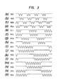
- the electrical resistance values of the magnetoresistive elements R0l to R34 varies as shown in Figs. 3(a) to (p) in response to the magnetic field applied thereto, which depends on the pattern of the magnetic signals recorded on the corresponding tracks TKl to TK8.
- the elements R0l to R34 form four bridge circuits B0 to B3 corresponding to the channels CH0 to CH3 respectively, as shown in Fig. 4.
- signals E0 to E3 of the rectangular waveform as shown in Figs. 6a to 6d are obtained by the known waveform shaping technique.
- the signals E0 to E3 constitute the values of respective digits of a digital position detecting signal of four bits, i.e., in this case, E0 corresponds to the least significant digit (LSD) of the four-bit signal and E3 to the most significant digit (MSD) thereof.
- LSD least significant digit
- MSD most significant digit
- the signals shown in Figs. 6a to 6d are formed in accordance with the so called gray code system. It is of course that other code systems such as a binary code system can be employed. To this end, the pattern of the magnetic signals recorded on the drum 6 has to be altered in accordance with the code system adopted. Also the number of bits of the position detecting signal has no particular limitation and can be selected as needed.
- Fig. 7 shows the arrangement and connection of the magnetoresistive elements and the wiring.
- the magnetoresistive elements R0l to R34 which are made of magnetic material such as Permalloy, are arranged on a base plate l8 made of glass by the vapor deposition.
- Wiring conductors Ll to L22 made, for example, of chromium are also provided on the base plate l8 by the vapor deposition.
- Tl to T8 and Tl9 to T22 indicate terminals connecting the elements R0l to R34 with an external circuit
- points indicated by reference symbols of the combination of a capital letter C and a numeral represent coupling points at which two wiring conductors are coupled to each other.
- the magnetoresistive elements R0l to R34 are formed as one body for the respective one of the two sets of the elements, i.e., the first set consisting of R0l, R03, Rll, Rl3, R2l, R23, R3l and R33, and the second set of R02, R04, Rl2, Rl4, R22, R24, R32, and R34.
- a magnetoresistive element body (a hatched portion) generally denoted by reference symbol R is made of Permalloy as a whole and comprises a long and slender portion 20, lead portions 22 projected from the slender portion 20 at the predetermined interval and terminal portions 24 provided at one ends of the lead portions 22 for connecting the wiring conductors Ll0, L8, Ll2.
- the slender portion 20 is functionally divided into plural segments by the lead portions 22; eight segments in the embodiment of Fig. 7.
- Each segment functions as the element R0l, R03, Rll, Rl3, R2l, R23, R3l or R33 in the first set of the magnetoresistive elements, or as the element R02, R04, Rl2, Rl4, R22, R24, R32 or R34 in the second set of the magnetoresistive elements.
- the wiring conductors Ll0, L8, Ll2 are connected to the respective terminal portions 24, the terminal portion 24 can be extended to function as a part of the wiring conductors as shown by an example of the wiring conductor Ll7 in Fig. 8.
- FIGs. 9a to 9c the sectional structure of the magnetic sensor 8 is shown.
- Figs. 9b and 9c are sectional views of the magnetic sensor 8 sectioned along section lines A-A and B-B in Fig. 9a, respectively.
- the magnetoresistive elements R0l to R34 and the wiring conductors Ll to Ll8 connected to the associated elements R0l to R34 constitute a first wiring layer, which is covered by insulating material (a first insulation layer) 26 such as silicon dioxide.
- insulating material (a first insulation layer) 26 such as silicon dioxide.
- the wiring conductors Ll9 to L22 which constitute a second wiring layer.
- the second wiring layer is also covered by insulating material (a second insulation layer) 28 such as silicon dioxide.
- the magnetic sensor 8 faces the drum 6 on the side of the second insulation layer 28.
- the element R0l facing the track TKl of the channel CH0 and the element R03 facing the track TK2 of the same channel, both belonging to the first set of the magnetoresistive elements, are arranged on the base plate l8 and structurally coupled with each other at adjacent ends thereof, as illustrated in Fig. 8. Another end of the element R0l, which is opposite to the coupled end thereof, is connected to the conductor L9 of the first wiring layer, which is further coupled to the conductor Ll9 of the second wiring layer at the coupling point Cl.
- the conductor Ll9 is led to the terminal Tl9, to which the positive side of the source l6 is coupled.
- Another end of the element R03, which is opposite to the coupled end thereof, is connected to the conductor Lll of the first wiring layer, which is further coupled to the conductor L20 of the second wiring layer at the coupling point C3.
- the conductor L20 is led to the terminal T20, to which the negative side of the source l6 is coupled.
- the element R02 facing the track TKl together with the element R0l and the element R04 facing the track TK2 together with the element R03, which belong to the second set of the magnetoresistive elements, are provided on the base plate l8 by ⁇ /2 apart from the elements R0l and R03 and structurally coupled with each other at adjacent ends thereof.
- Another end of the element R02, which is opposite to the coupled end thereof, is connected to the conductor Ll0 of the first wiring layer, which is further coupled to the conductor L2l of the second wiring layer at the coupling point C2.
- the conductor L2l is led to the terminal T2l, which is coupled in common with the terminal T20 to the negative side of the source l6.
- Another end of the element R04 which is opposite to the coupled end thereof, is connected to the conductor Ll2 of the first wiring layer, which is further coupled to the conductor L22 of the second wiring layer at the coupling point C4.
- the conductor 22 is led to the terminal T22, to which the positive side of the source l6 is coupled.
- the magnetoresistive elements R0l to R04 form the bridge circuit B0 shown in Fig. 4.
- the coupling points of the structurally coupled elements R0l and R03, and R02 and R04 are connected to the terminals Tl and T8 through the conductors Ll and L8 provided in the first wiring layer, respectively.
- These terminals Tl and T8 serve as output terminals of the bridge circuit B0.
- the output voltage e0 of the circuit B0 appears across the terminals Tl and T8.
- the same as described above of the magnetoresistive elements R0l to R04 is applied to the arrangement of the elements Rll to Rl4 facing the tracks TK3 and TK4 of the channel CHl and the wiring conductors associated therewith.
- These elements Rll to Rl4 form the bridge circuit Bl shown in Fig. 4, and the output voltage el appears across the terminals T2 and T7.
- the elements R2l to R24 form the bridge circuit B2 and the output voltage e2 appears across the terminals T3 and T6.
- the elements R3l to R34 form the bridge circuit B3 and the output voltage e3 appears across the terminals T4 and T5.
- the conductors Lll and Ll2, Ll3 and Ll4, and Ll5 and Ll6 are selectively coupled to the conductors Ll9, L20, L2l and L22 and employed in common for supplying the adjacent bridge circuits with source voltage. Further, the conductors Ll9 to L22 and the terminals Tl9 to T22 associated therewith are arranged inside the conductors Ll to L8 for deriving the output voltages from the magnetoresistive elements R0l to R34 and the terminals Tl to T8 associated therewith, when viewed from the side of the magnetoresistive elements.
- any conductors for deriving the output voltages i.e., Ll to L8, do not cross with one another, so that the output voltages of the bridge circuits B0 to B3 do not interfere with one another and therefore the resistivity against noise caused by any other bridge circuit is much enhanced.
- the electrical resistance of the wiring for supplying the magnetoresistive elements R0l to R34 with the source voltage is as low as possible so that the output voltages e0 to e3 of the bridge circuits B0 to B3 become as large as possible.
- An example of the arrangement of the wiring conductors suited therefor is shown in Fig. l0, in which the same reference symbols indicate the same parts as in Fig. 7. To facilitate matters, only the conductors L9 to L22 for voltage supply are shown and the conductors for deriving the output voltages from the magnetoresistive elements are omitted. Further, since the connection of the elements R0l to R34 and the conductors L9 to L22 is quite the same as that in Fig. 7, the further description thereof is also omitted here. As apparent from the figure, the conductors Ll9 to L22 are very wide, compared with those in Fig. 7. Therefore, the electrical resistance of the wiring for voltage supply can be reduced remarkably.
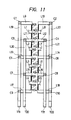
- Fig. ll shows another example of the arrangement and connection of the magnetoresistive elements R0l to R34 and the conductors L9 to L22 for voltage supply.
- the same reference symbols in this figure indicate the same parts as in Fig. 7.
- the arrangement and connection of the conductors Ll to L8 for deriving the output voltages from the magnetoresistive elements R0l to R34 are the same as in Fig. 7, although they are not shown in this figure.
- the terminals Tl9 to T22 for voltage supply are so arranged that the terminals Tl9 and T2l to be coupled to the positive electrode of the source l6 and the terminals T20 and T22 to be coupled to the negative electrode thereof alternate regularly.
- the polarities of the terminals are scarcely confused and the erroneous wiring can be prevented.
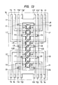
- Fig. l2 shows the arrangement and connection of the magnetoresistive elements and the wiring conductors according to another embodiment of the present invention.
- the same reference symbols indicate the same parts as in Fig. 7.
- the elements R0l to R34 are formed in the same manner as shown in Fig. 8.
- the element R0l facing the track TKl of the channel CH0 and the element R03 facing the track TK2 of the same channel, which belong to the first set of the magnetoresistive elements, are structurally coupled with each other at adjacent ends thereof and further connected to the terminal Tl through the conductor Ll.
- the conductor L9 which is extended to the outside of the conductor Ll, when viewed from the side of the magnetoresistive elements.
- the conductor L9 is connected to the conductor Ll9 at the coupling point Cl and led to the terminal Tl9, to which the positive voltage is applied from the source l6.
- Another end of the element R03 which is opposite to the coupled end thereof, is connected to the conductor Lll, which is also extended to the outside of the conductor Ll.
- the conductor Lll is connected to the conductor L20 at the coupling point C3 and led to the terminal T20, which is connected to the negative terminal of the source l6.
- the element R02 facing the track TKl and the element R04 facing the track TK2, which belong to the second set of the magnetoresistive elements, are also structurally coupled with each other at adjacent ends thereof and further connected to the terminal T8 through the conductor L8.
- Another end of the element R02, which is opposite to the coupled end thereof, is connected to the conductor Ll0, which is extended to the outside of the conductor L8, when viewed from the side of the magnetoresistive elements.
- the conductor Ll0 is connected to the conductor L2l at the coupling point C2 and led to the terminal T2l, to which the negative voltage is applied by the source l6.
- the conductor Ll2 To another end of the element R04, which is opposite to the coupled end thereof, is connected the conductor Ll2 which is also extended to the outside of the conductor L8.
- the conductor Ll2 is connected to the conductor L22 at the coupling point C4 and led to the terminal T22 which is connected to the positive terminal of the source l6.
- the magnetoresistive elements R0l to R04 form the bridge circuit B0 shown in Fig. 4 and the terminals Tl and T8 serve as the output terminals of the bridge circuit B0, across which the output voltage e0 appears.
- the magnetoresistive elements Rll to Rl4, R2l to R24 and R3l to R34 are arranged and connected in the same manner as described above and form the bridge circuits Bl to B3, which produce the output voltages el to e3, respectively. It is to be noted that, in the structure of Fig.
- the terminals Tl9 to T22 for voltage supply (and therefore the conductors Ll9 to L22, too) are positioned outside the terminals Tl to T8 for deriving the output voltages from the bridge circuits (and therefore the conductors Ll to L8, too).
- the conductors for voltage supply are provided as outermost wiring of the arrangement of the magnetic sensor 8. Accordingly, it is possible to prevent external noise from entering the conductors Ll to L8 and the terminals Tl to T8.
- Fig. l3 is a drawing showing the arrangement and connection of the magnetoresistive elements and the wiring according to a further embodiment of the present invention.
- the same reference symbols denote the same parts as in the foregoing embodiments.
- the arrangement of the magnetoresistive elements R0l to R34 and the connection of the wiring conductors Ll to L22 in this embodiment are basically the same as in Fig. 7.
- the upper side of the base plate l8 is a most accessible side to the elements R0l to R04 and Rll to Rl4, and the lower side thereof is that to the elements R2l to R24 and R3l to R34.
- terminals are provided on the side of a magnetic sensor, which is most accessible to the magnetoresistive elements associated with the terminals.
- the terminals Tl9 to T22 and Tl9' to T22' for voltage supply are arranged on both the sides of the base plate l8. With this structure, the width of the magnetic sensor 8 can be made smaller.
- two among the magnetoresistive elements forming a certain bridge circuit which are brought into a line on the base plate, are coupled with each other at the adjacent ends thereof and the coupling point serves as one of terminals for deriving the output voltage of the certain bridge circuit.
- Opposite ends of the elements are employed as terminals for voltage supply.
- the relationship of these terminals may be inverted. Namely, the bridge circuit is supplied with voltage at the coupling point of the elements and the output voltage can be derived from the opposite ends of the elements.
- Fig. l4 shows an embodiment of such a type.
- the same reference symbols indicate the same parts as in the foregoing embodiments, and other reference symbols will be referred to in the following description of the structure and operation of this embodiment.
- the magnetoresistive elements are formed for every channels separately.
- the elements R0l and R03 which belong to the first set of the magnetoresistive elements, are formed as one body on the base plate l8, and the coupling point thereof is connected to the conductor L9.
- the conductor L9 is connected to a conductor LP at the coupling point Cl.
- the conductor LP is connected to a terminal TP, to which the positive voltage of the source l6 is applied.
- the elements R02 and R04 which belong to the second set of the magnetoresistive elements, are also formed as one body on the base plate l8, but by half the pitch ( ⁇ /2) apart form the first set of the elements R0l and R03.
- the coupling point thereof is connected to the conductor Ll0.
- the conductor Ll0 is connected to a conductor LN, to which the negative voltage of the source l6 is applied through a terminal TN.
- the respective ends of the elements R0l to R04 opposite to the coupled ends are connected to terminals Tl, T8, Tl' and T8' through conductors Ll, L8, Ll' and L8'
- the terminals Tl and T8', and Tl' and T8 are externally connected with each other respectively to form two output terminals of a bridge circuit B0 corresponding to the channel CH0.
- the bridge circuit B0 in this case is so modified that the element R03 in the bridge circuit B0 shown in Fig. 4 changes place with the element R04. However, it is operationally the same as the bridge circuit B0 of Fig. 4.
- the remaining bridge circuits Bl, B2 and B3 corresponding to the channels CHl, CH2 and CH3 are constructed in the same manner.
- the connection of the wiring shown in Fig. l4 has the disadvantage of the increased number of terminals, it becomes simple in the arrangement of the conductors, compared with the foregoing embodiments.
- the terminals associated with the conductors for deriving the output voltages from the magnetoresistive elements are so arranged on the base plate of the magnetic sensor that the terminals corresponding to the channel which is most remote from the side on which the terminals are provided, are positioned as the outermost terminals. Thereby, there are no crossing points of the conductors and therefore the mutual interference by the output voltages between the channels can be decreased.
- the position detector is formed by the rotary drum with the magnetic signals recorded thereon and the sensor for detecting the magnetic signals recorded on the drum, whereby the position of a rotating body can be detected.
- the present invention can be also applied to a position detector, in which the rotary drum is substituted by a linearly moving member, on which the magnetic signals of the pattern as shown in Fig. 2 are recorded. With such a position detector, the position of a linearly moving body can be detected directly without converting the linear movement into the rotating one.
Landscapes
- Physics & Mathematics (AREA)
- General Physics & Mathematics (AREA)
- Engineering & Computer Science (AREA)
- Theoretical Computer Science (AREA)
- Transmission And Conversion Of Sensor Element Output (AREA)
- Measurement Of Length, Angles, Or The Like Using Electric Or Magnetic Means (AREA)
Applications Claiming Priority (2)
| Application Number | Priority Date | Filing Date | Title |
|---|---|---|---|
| JP60223567A JPH0638047B2 (ja) | 1985-10-09 | 1985-10-09 | 磁気的に位置を検出する装置 |
| JP223567/85 | 1985-10-09 |
Publications (2)
| Publication Number | Publication Date |
|---|---|
| EP0218242A2 true EP0218242A2 (fr) | 1987-04-15 |
| EP0218242A3 EP0218242A3 (fr) | 1989-04-05 |
Family
ID=16800182
Family Applications (1)
| Application Number | Title | Priority Date | Filing Date |
|---|---|---|---|
| EP86113925A Withdrawn EP0218242A3 (fr) | 1985-10-09 | 1986-10-08 | Appareil de détection magnétique de la position d'un corps |
Country Status (3)
| Country | Link |
|---|---|
| US (1) | US4786870A (fr) |
| EP (1) | EP0218242A3 (fr) |
| JP (1) | JPH0638047B2 (fr) |
Cited By (3)
| Publication number | Priority date | Publication date | Assignee | Title |
|---|---|---|---|---|
| EP0369031A1 (fr) * | 1988-05-30 | 1990-05-23 | Fanuc Ltd. | Codeur de position absolue |
| EP0382856A1 (fr) * | 1988-07-29 | 1990-08-22 | Fanuc Ltd. | Codeur magnetique de position absolue |
| EP2267413A1 (fr) * | 2008-03-25 | 2010-12-29 | Alps Electric Co., Ltd. | Détecteur magnétique et codeur magnétique |
Families Citing this family (19)
| Publication number | Priority date | Publication date | Assignee | Title |
|---|---|---|---|---|
| US4860432A (en) * | 1986-09-02 | 1989-08-29 | Alps Electric Co., Ltd. | Method of manufacturing a magnetoresistive sensor |
| JPH02271216A (ja) * | 1989-04-13 | 1990-11-06 | Hitachi Metals Ltd | 磁気式エンコーダ |
| JP2787783B2 (ja) * | 1990-06-08 | 1998-08-20 | ソニー・プレシジョン・テクノロジー株式会社 | 位置検出装置 |
| US5293125A (en) * | 1992-01-17 | 1994-03-08 | Lake Shore Cryotronics, Inc. | Self-aligning tachometer with interchangeable elements for different resolution outputs |
| EP0555961B1 (fr) * | 1992-02-13 | 1997-07-16 | Japan Servo Co. Ltd. | Codeur absolu |
| JP3063044B2 (ja) * | 1992-02-13 | 2000-07-12 | 日本サーボ株式会社 | アブソリュートエンコーダ |
| US5336994A (en) * | 1992-11-20 | 1994-08-09 | Lake Shore Cryotronics, Inc. | Magneto-resistive tachometer assembly with reversible cover and related method |
| US5444370A (en) * | 1993-03-18 | 1995-08-22 | Honeywell Inc. | Magnetic angular position sensor with two magnetically sensitive components arranged proximate two target tracks having complimentary magnetic and nonmagnetic segments |
| US5495758A (en) * | 1993-06-17 | 1996-03-05 | Lake Shore Cryotronics, Inc. | Tachometer assembly with integral internal wrench |
| US5514955A (en) * | 1994-03-11 | 1996-05-07 | Lake Shore Cryotronics, Inc. | Slim profile digital tachometer including planar block and rotor having spokes and clamp |
| US5502380A (en) * | 1994-04-28 | 1996-03-26 | Rosemount Inc. | Analog weighted binary absolute position encoder including an array of sense resistors each having material responsive to FWX and nonresponsive to flux |
| US6246233B1 (en) | 1994-12-30 | 2001-06-12 | Northstar Technologies Inc. | Magnetoresistive sensor with reduced output signal jitter and temperature compensation |
| US5900930A (en) * | 1997-10-21 | 1999-05-04 | Eaton Corporation | Angle sensor using a multi-pixel optical device |
| US6305229B1 (en) * | 1997-12-23 | 2001-10-23 | Tanaka Systems Incorporated | Detecting fatigue from magnetic characteristics |
| FR2795507B1 (fr) * | 1999-06-24 | 2001-08-03 | Roulements Soc Nouvelle | Capteur de couple a barrette de hall |
| JP4723821B2 (ja) * | 2003-06-13 | 2011-07-13 | 株式会社フジコー | 非粘着性のフェルト材とその製造法 |
| DE10330986B4 (de) * | 2003-07-09 | 2010-01-07 | Tecpharma Licensing Ag | Berührungslose Abtastung mit magnetoresistivem Sensor |
| JP4586800B2 (ja) * | 2004-07-12 | 2010-11-24 | Nok株式会社 | 磁気エンコーダ |
| WO2015029736A1 (fr) * | 2013-08-29 | 2015-03-05 | アルプス・グリーンデバイス株式会社 | Capteur de courant |
Citations (3)
| Publication number | Priority date | Publication date | Assignee | Title |
|---|---|---|---|---|
| GB2016144A (en) * | 1978-03-06 | 1979-09-19 | Nippon Electric Co | Magnetic rotary encoder for detection of absolute values of angular displacement |
| EP0098551A2 (fr) * | 1982-07-02 | 1984-01-18 | Hitachi, Ltd. | Capteur de position magnétique |
| EP0111866A2 (fr) * | 1982-12-13 | 1984-06-27 | Hitachi, Ltd. | Appareil pour la détection magnétique de positions |
Family Cites Families (1)
| Publication number | Priority date | Publication date | Assignee | Title |
|---|---|---|---|---|
| JPS59105503A (ja) * | 1982-12-09 | 1984-06-18 | Fanuc Ltd | 磁気パルスエンコーダ用の磁気抵抗効果素子が装着された回路板 |
-
1985
- 1985-10-09 JP JP60223567A patent/JPH0638047B2/ja not_active Expired - Lifetime
-
1986
- 1986-10-08 US US06/916,699 patent/US4786870A/en not_active Expired - Fee Related
- 1986-10-08 EP EP86113925A patent/EP0218242A3/fr not_active Withdrawn
Patent Citations (3)
| Publication number | Priority date | Publication date | Assignee | Title |
|---|---|---|---|---|
| GB2016144A (en) * | 1978-03-06 | 1979-09-19 | Nippon Electric Co | Magnetic rotary encoder for detection of absolute values of angular displacement |
| EP0098551A2 (fr) * | 1982-07-02 | 1984-01-18 | Hitachi, Ltd. | Capteur de position magnétique |
| EP0111866A2 (fr) * | 1982-12-13 | 1984-06-27 | Hitachi, Ltd. | Appareil pour la détection magnétique de positions |
Cited By (6)
| Publication number | Priority date | Publication date | Assignee | Title |
|---|---|---|---|---|
| EP0369031A1 (fr) * | 1988-05-30 | 1990-05-23 | Fanuc Ltd. | Codeur de position absolue |
| EP0369031A4 (en) * | 1988-05-30 | 1991-12-27 | Fanuc Ltd | Absolute position encoder |
| EP0382856A1 (fr) * | 1988-07-29 | 1990-08-22 | Fanuc Ltd. | Codeur magnetique de position absolue |
| EP0382856A4 (en) * | 1988-07-29 | 1991-01-09 | Fanuc Ltd | Magnetic absolute position encoder |
| EP2267413A1 (fr) * | 2008-03-25 | 2010-12-29 | Alps Electric Co., Ltd. | Détecteur magnétique et codeur magnétique |
| EP2267413A4 (fr) * | 2008-03-25 | 2014-06-11 | Alps Electric Co Ltd | Détecteur magnétique et codeur magnétique |
Also Published As
| Publication number | Publication date |
|---|---|
| EP0218242A3 (fr) | 1989-04-05 |
| JPH0638047B2 (ja) | 1994-05-18 |
| US4786870A (en) | 1988-11-22 |
| JPS6283619A (ja) | 1987-04-17 |
Similar Documents
| Publication | Publication Date | Title |
|---|---|---|
| EP0218242A2 (fr) | Appareil de détection magnétique de la position d'un corps | |
| US4774464A (en) | Magnetic rotary sensor for detecting absolute position of rotating body | |
| EP0555961B1 (fr) | Codeur absolu | |
| US5519393A (en) | Absolute digital position encoder with multiple sensors per track | |
| EP0098551B1 (fr) | Capteur de position magnétique | |
| US5880683A (en) | Absolute digital position encoder | |
| US4429276A (en) | Magnetoresistive displacement sensor and signal reprocessing circuits therefor | |
| EP0212578B1 (fr) | Détecteur de position absolue | |
| US4603365A (en) | Magnetic detection apparatus | |
| EP0111866B1 (fr) | Appareil pour la détection magnétique de positions | |
| US4853631A (en) | Magnetoresistive sensor having inter-leaved magnetoresistive elements for detecting encoded magnetic information | |
| JP4204328B2 (ja) | 基準点を基準とするピストンロッドの絶対位置の検出のための測定システムを有する圧力媒体シリンダ | |
| JPH0623931Y2 (ja) | 磁気スケール用検出器 | |
| US5821517A (en) | Magnetic encoder for reading marks on an associated magnetic track | |
| US3452358A (en) | Magnetically encoded device | |
| US4806860A (en) | Overlapped magnetoresistive displacement detecting transducers having closely spaced longitudinal centers | |
| US4757257A (en) | Magnetoresistive displacement sensor and signal processing circuit | |
| JP3063044B2 (ja) | アブソリュートエンコーダ | |
| JP2979692B2 (ja) | 磁気エンコーダ | |
| JPH0820271B2 (ja) | 位置や速度を検出する装置 | |
| JPH03285113A (ja) | 電源投入時に絶対位置の検出が可能な1トラック型アブソリュートエンコーダ | |
| JP2691942B2 (ja) | ロータリー式アブソリュートエンコーダ | |
| JPS5821158A (ja) | 多チヤネル磁気センサ | |
| JP2961462B2 (ja) | アブソリュートエンコーダ | |
| JP3023248B2 (ja) | 位置検出装置 |
Legal Events
| Date | Code | Title | Description |
|---|---|---|---|
| PUAI | Public reference made under article 153(3) epc to a published international application that has entered the european phase |
Free format text: ORIGINAL CODE: 0009012 |
|
| 17P | Request for examination filed |
Effective date: 19861008 |
|
| AK | Designated contracting states |
Kind code of ref document: A2 Designated state(s): CH DE FR GB IT LI NL SE |
|
| PUAL | Search report despatched |
Free format text: ORIGINAL CODE: 0009013 |
|
| AK | Designated contracting states |
Kind code of ref document: A3 Designated state(s): CH DE FR GB IT LI NL SE |
|
| 17Q | First examination report despatched |
Effective date: 19901026 |
|
| STAA | Information on the status of an ep patent application or granted ep patent |
Free format text: STATUS: THE APPLICATION IS DEEMED TO BE WITHDRAWN |
|
| 18D | Application deemed to be withdrawn |
Effective date: 19921020 |
|
| RIN1 | Information on inventor provided before grant (corrected) |
Inventor name: MIYASHITA, KUNIO Inventor name: TAKAHASHI, TADASHI Inventor name: KAWAMATA, SYOOICHI |