EP0215397A2 - Vorrichtung zum Abschälen eines Films - Google Patents
Vorrichtung zum Abschälen eines Films Download PDFInfo
- Publication number
- EP0215397A2 EP0215397A2 EP86112301A EP86112301A EP0215397A2 EP 0215397 A2 EP0215397 A2 EP 0215397A2 EP 86112301 A EP86112301 A EP 86112301A EP 86112301 A EP86112301 A EP 86112301A EP 0215397 A2 EP0215397 A2 EP 0215397A2
- Authority
- EP
- European Patent Office
- Prior art keywords
- films
- board
- film
- peeling
- members
- Prior art date
- Legal status (The legal status is an assumption and is not a legal conclusion. Google has not performed a legal analysis and makes no representation as to the accuracy of the status listed.)
- Granted
Links
Images


Classifications
-
- G—PHYSICS
- G03—PHOTOGRAPHY; CINEMATOGRAPHY; ANALOGOUS TECHNIQUES USING WAVES OTHER THAN OPTICAL WAVES; ELECTROGRAPHY; HOLOGRAPHY
- G03F—PHOTOMECHANICAL PRODUCTION OF TEXTURED OR PATTERNED SURFACES, e.g. FOR PRINTING, FOR PROCESSING OF SEMICONDUCTOR DEVICES; MATERIALS THEREFOR; ORIGINALS THEREFOR; APPARATUS SPECIALLY ADAPTED THEREFOR
- G03F7/00—Photomechanical, e.g. photolithographic, production of textured or patterned surfaces, e.g. printing surfaces; Materials therefor, e.g. comprising photoresists; Apparatus specially adapted therefor
- G03F7/16—Coating processes; Apparatus therefor
- G03F7/161—Coating processes; Apparatus therefor using a previously coated surface, e.g. by stamping or by transfer lamination
-
- B—PERFORMING OPERATIONS; TRANSPORTING
- B29—WORKING OF PLASTICS; WORKING OF SUBSTANCES IN A PLASTIC STATE IN GENERAL
- B29C—SHAPING OR JOINING OF PLASTICS; SHAPING OF MATERIAL IN A PLASTIC STATE, NOT OTHERWISE PROVIDED FOR; AFTER-TREATMENT OF THE SHAPED PRODUCTS, e.g. REPAIRING
- B29C63/00—Lining or sheathing, i.e. applying preformed layers or sheathings of plastics; Apparatus therefor
- B29C63/0004—Component parts, details or accessories; Auxiliary operations
- B29C63/0013—Removing old coatings
Definitions
- This invention relates to an apparatus for peeling off films and more particularly to a technique effective in peeling off protective films stuck onto a board and used to protect the faces thereof.
- Printed circuit boards for use in electronic equipment such as computers are provided with a predetermined copper wiring pattern formed on one or both sides of an insulating substrate.
- a printed circuit board of that sort is manufactured through a process comprising the steps of laminating a photosentitive resin layer (photoresist) and a translucent resin film (protective film) for protecting the photosentitive resin layer on a conductive layer laid on an insulating substrate through thermocompression bonding: superposing a film having a wiring pattern; exposing the photosensitive resin layer to light for a fixed period of time through the film having the wiring pattern and the translucent resin film; developing the thus exposed photosentitive resin layer after peeling off the translucent resin film to form an etching mask pattern; removing unnecessary-portions of the conductive layer by etching; and further removing the remaining photosensitive resin layer.
- a printed circuit board having a prodetermined wiring pattern is thus prepared.
- the translucent resin film In the above steps of manufacturing a printed circuit board, the translucent resin film must be peeled off when the photosensitive resin layer is developed after being exposed to light. That step of peeling off the translucent resin film still relies on manual work, which requires a clever-fingered worker as well as an extremely skilled hand to prevent damage and breakdown attributed to unevenly distributed peel stress because the film is thin.
- the problem is that lengthy work is required in the manufacture of a printed circuit board because it takes time to peel off the translucent resin film.
- the peeling apparatus for peeling off films stuck onto a board comprises press members for pressing the end surfaces of the films stuck onto the board, fluid spray means for sending jets of fluid to the portions to which the force has been applied, and film peeling guide members for setting peel directions by changing the peel angles of the films peeled off the board using the fluid spray means with the board with in the range of an obtuse angle and causing the films thus peeled off to attach thereto, or film discharge means for discharging the films guided with the aid of the film peeling guide means.
- a gap is formed under the end of each film by applying force thereto using the press member and a jet of fluid is sent to that end portion to ensure that the film is instantly peeled off.
- the film is supplied with uniform peeling and a stabilized peel position, so that the film is made free from damage or breakdown and peeled off the board at the peel angle. Since the angle of each film peeling guide member is variable, the film can be peeled off at an optimum peel angle.
- the film discharge means for discharging the film stuck onto the film peeling guide member contributes to automatic film peeling and thus a saving in film peeling time by a large margin.
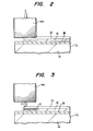
- Fig. 1 is a sectional view outlining the construction of a peeling apparatus for peeling off protective films as an embodiment of the present invention.
- a mechanism for conveying a printed circuit board 1 in the peeling apparatus for peeling off the protective films comprises conveyor rollers 2 for carrying the printed circuit board 1 and conveyance control rollers 3.
- the printed circuit board 1 is formed of conductive layers 1B of copper stuck onto both sides (or one side) of an insulating substrate 1A.
- Laminated bodies each consisting of a photosensitive resin layer 1C and a translucent (protective) resin film 1D, are stuck onto the conductive layers 1B of the printed circuit board 1 through thermocompression bonding.
- the photosensitive resin layers 1C are in such a state that they have been exposed to light so as to form a predeterminated pattern.
- the conveyor rollers 2 and the conveyance control rollers 3 are so arranged as to carry the printed circuit board 1 in the direction of an arrow in the conveyance path whose view is taken on line A-A of Fig. 1.
- Each press mechanism 4 shown in Figs. 1 through 6 is so arranged as to apply force to the end face of the translucent resin film 1D of the printed circuit board 1 with a press member 4A provided with knurls on its rotary body.
- the press member 4A is prepared from, e.g., highspeed steel.
- the printed circuit board 1 being conveyed is stopped in between a pair of the upper and lower press members 4A.
- the position of the printed circuit board 1 is controlled by the position detectors S and the conveyance control rollers 3.
- Each position detector S is formed of a photosensor.
- the position of the printed circuit hoard 1 may be controlled by stopper members each controlled by the position detectors S.
- each press member 4A comprises a pair of support members 4B laterally installed in the direction roughly perpendicular to the conveyance direction of the translucent resin film 10, a pair of arm members 4C rotatable and movable in the direction of an arrow B and a pair of press member support members 4E made movable by air cylinders 4D in the direction of an arrow C.
- the press member support member 4E and the arm member 4C are so combined as to move linearly in the direction of the arrow C and rotate in the direction of the arrow B. In order to smooth the movement of both members, a proper clearance is provided for the rotary shaft of the arm member 4C.
- the press members 4A are moved or reciprocated in the direction of an arrow D which is roughly prependicular to the conveyance direction of the press members 4A while the front face of the translucent resin film 1D is pressed.
- each press member 4A is so arranged as to apply force to the roughly whole area of the front face (end face of the one side of the front portion in the conveyance direction) of the square translucent resin film 1D.
- the movement of the press member 4A in the direction of the arrow D causes a pair of guide rails 4F to slide, the sliding movement is implemented by an air cylinder 4H installed on one side of the slide member 4G and a rack 4J installed on each slide member 4G coupled to a pinion 4I.
- the above pinion 4I and the rack 4J are so arranged as to slide the other slide member 4G (on the left of Fig. 6) in the direction opposite to one slide member 4G (on the right of Fig. 6) slid by the air cylinder 4H.
- the engagement of the pinion 4I and the rack 4J are kept stably by a guide roller 4K.
- the air cylinder 4D releases the press member 4A with a resilient member (not shown).
- the air cylinders 4D, 4H may be replaced with hydraulic or other liquid cylinders, whereas the pinion 4I and the rack 4J may be replaced with other belt mechanisms.
- the gap can thus be formed between the photosensitive resin layer 1C and the translucent resin film 1D as shown in Fig. 3 by applying force to the end face of the translucent resin film 1D of the printed circuit board 1 with the press member 4A.
- the reason for the formation of the gap is that the material for the photosensitive resin layer 1C is different from that for the translucent resin film 1D and, if the former is readily subjected to plastic deformation as compared with the latter, the adhesion there between is nullified by the shearing force applied thereto.
- the press member 4A installed in the conveyance path of the printed circuit board 1 allows the formation of the gap automatically between the photosensitive resin layer 1C and the translucent resin film ID.
- the gap formed between the photosensitive resin layer 1C and the translucent resin film 1D is squeezed by the conveyor rollers 2 or conveyance control rollers 3 while the printed circuit board 1 is carried out by the fluid spray mechanism 5, the photosensitive resin layer 1C and the translucent resin fil 1D will not be bound together again because they have not been treated with thermocompression bonding.
- the press member 4A is made to slide on the almost whole area along one side while the end face of the translucent resin film 1D is being pressed, it may be made to slide on only the narrow part thereof. However, the press member 4A must be made to slide on the place in whice the fluid is sprayed by the fluid spray mechanism 5. translucent resin film 1D is being pressed, it may be made to slide on only the narrow part thereof. However, the press member 4A must be made to slide on the place in which the fluid is sprayed by the fluid spray mechanism 5.
- the fluid spray mechanism 5 is so arranged as to sent pressurized fluid such as air, inert gas and liquid such as water from a nozzle 5A and a Jet of fluid directly to the gap between the translucent resin film ID of the printed circuit board 1 and the photosensitive resin layer 1C (of the board).
- pressurized fluid such as air, inert gas and liquid such as water
- the nozzle 5A may be so arranged as shown by 5A' of Fig. 7 to make its set angle variable.
- the translucent resin film 1D is thus peeled off simply, surely and accurately by sending a jet of fluid to the gap produced by by the press member 4A between the tranlucent resin film 1D and the photosensitive layer 1C using the fluid spray mechanism 5.
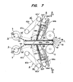
- Each film discharge mechanism 6 consists of a fixed belt conveyor 6A, a film peeling guide member 6B, a moving belt conveyor 6C and a belt mechanism 6D for carrying the film out.
- Each belt conveyor 6A as shown in Figs. 1, 7 and 8, consists of a plurality of pairs of rollers 6Aa, 6Aa', and a belt 6Ab wound on each pair of rollers 6Aa, 6Aa l .
- Each film peeling guide 6B is installed in the case of the film peeling apparatus on the fixed belt conveyor side 6A and the belt 6Ab is allowed to slide on part of the guide face.
- the film peeling guide member 63 is so arranged that the angle of the printed circuit board 1 deprived of the film with the translucent resin film ID is allowed to vary.within the range of an obtuse angle to hold the translucent resin film 1D thus peeled off to a satisfactory extent.
- the angle at which the film is peeled ranges from 100 to 170 degrees and made variable within that range.
- the variation of the peel angle by means of the film peeling guide member 6B can be executed by the mechanical means such as gears, crank mechanisms and the like or electrical means such as step-motors. similarly, the film peeling guide member 6B may be move linearly as indicated by the arrous Q in Figs. 7 and 8.
- the film peeling guide member 6B set at an obtuse angle so as to minimuze the force applied to the photosensitive resin layer 1C freed from the translucent resin film 1D is capable of preventing damage and breakdown to any photosensitive resin layer 1C.
- an optimum peel angle can be set in correspondence with the film peel rate and peeling, so that any optimum peel angle can be set, irrespective of the printed circuit board 1 or film peeling condition.
- the film peeling guide member 63 is so constructed as to make the translucent resin film lD peeled off by the fluid spray mechanism 5 attach thereto by the indirect fluid pressure derived from the fluid spray mechanism or static electricity generated when the film is peeled off.
- Each moveing belt conveyor 6C consists, as shown in Figs. 1, 7, a pair of rollers 6Ca, 6Ca' and a belt 6Cb on the pair of the rollers 6Ca, 6Ca'.
- the moving belt conveyor 6C is moved by the air cylinder 6Cc with the roller 6Ca' as the center and so arranged as to move close to or come in contact with the belt 6Ab of the fixed belt conveyor 6A or film peeling guide member 6B.
- the moving belt conveyor 6C is made to ensure that the translucent resin film 1D thus peeled off by the fluid spray mechanism 5 is held and transferred by the film peeling guide member 6B.
- Each film discharge mechanism 6 is composed of the fixed belt conveyor 6A, the film peeling guide member 6B and the moving belt conveyor 6C, so that it becomes possible to make the translucent resin film 1D peeled off by the fluid spray mechanism 5 attach to the film peeling guide member 6B and have the translucent resin film 1D firmly held in between the fixed and moving belt conveyors 6A, 6C and carried out in the direction of an arrow OUT in Fig. 7.
- the film discharge mechanism 60 consists, as shown in Fig. 1, of a plurality of rollers 6Da and a pair of belts 6Db and is so arranged as to discharge the translucent resin film located on the upper side of the printed circuit board 1.
- the moving- belt conveyor 6C may be moved by a solenoid or hydraulic cylinder instead of the air cylinder 6Cc.
- the gap is formed under the translucent resin film 1D of the printed circuit board 1 and the fluid spray mechanism 5 is then used to peel off the translucent resin film 1D instantly to ensure that the translucent resin film thus peeled off is automatically carried out, so that the time required for the peeling work can be shortened by a large margin.
- the printed circuit board 1 is carried into a developing device by the conveyance control rollers 3 or and conveyor rollers 2.
- the press member 4A is employed to press the front face of the translucent resin film 1D of the printed circuit board 1 in its conveyance direction according to the above embodiment, it may also be used to press the end face thereof in the direction perpendicular to the conveyance direction thereof according to the present invention.
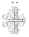
- Fig. 7A shows the guide mechanism 6 held in a state in which the film peeling member 6B is perpendicular to the board travel path.
- the film peeling guide member 6B is so designed that, in order to prevent the variation of the peeling position of the translucent resin film 1D, the variation of peeling stress thereof and to prevent the photosensitive resin layer 1C from being damaged or broken, guides the translucent resin film 1D in such a manner that the peeling angle of the latter 1D is obtuse with respect to the direction of conveyance of the printed circuit board 1.
- the speed of peeling and conveying the translucent resin.film 1D is made equal to the speed of conveyance of the printed circuit board 1, or at the start of peeling the speed of conveyance of the printed circuit board is made higher than the speed of peeling and conveying the translucent resin film 1D, so that the peeling angle of the translucent resin film 1D is obtuse with respect to the direction of conveyance of the printed circuit board 1.
- Figs. 9 and 10 show another embodiment of the present invention.
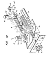
- Fig. 9 is a schematic view showing a positional relation of a board centering mechanism 7 interposed at a predetermined location of a board conveyor device II. As shown in Fig. 9 and 10, a centerline of the board 1 is aligned with a centerline of the board 1 is aligned with a centerline of the board travelling path in the conveyance direction. by the centering mechanism 7.
- the centering mechanism 7 inludes board aligning members 7B, 7B' carried on support members 7A and 7A'.
- the board aligning members 7B, 7B' are located so as to side edges of the board 1 travelling the board conveyance path A-A, so that the centerline of the board 1 is aligned with a centerline of the board conveyor device II.
- the board aligning members 7B and 7B' are in the form of cylinders but may be modified to any desired shapes such as planar plates.
- the support members 7A and 7A' are slidably mounted on respective support rods 7C.
- the support members 7A, 7A' are caused to cooperate with each other through a pinion 7D and racks 7E and 7E' which are coupled to the support members 7A and 7A', respectively.
- Connected to the support member 7A is an air cylinder 7F having an L-shaped member at its distal end.
- a screw rod 7J Engaged with a nut member 7H provided at a bottom of the frame 7G is a screw rod 7J that may be rotated by a controlling handle 7I.
- the rotation of the control handle 7I causes the frame 7G to move in the widthwise direction indicated by the arrow C.
- This moving or fine adjusting mechanism is available in the case where the centerlines of the board conveyance path and the centering mechanism 7 are displaced from each other.
- the fixing action of the moving mechanism may be carried out by a fastening screw 7i for stopping the rotation of the screw rod 7J.
- Sensors S 1 shown in Fig. 9 serve to detect a leading or trailing end of the board 1 and apply their signals to drive the board aligning members 7B, 7B' of the centering mechanism 7.
- the board position sensors S 1 are supported to a frame of the board conveyor device II.
- the sensors S 1 may be of the reflex type photosensor, for example.
- Board position sensors S 2 shown in Figs. 9 and 10 are adapted to detect the side edges of the board 1, thereby generate driving/stopping signals for the board aligning members 7B, 7B' of the centering mechanism 7.
- the sensors S 2 are located at the support members 7A, 7A' closer to the centerline than the aligning members 7B, 7B'.
- the aligning members 7B, 7B' are stopped by the signals from the sensors S 2 .
- the sensors S 2 may be of the transparent photosensor type but is not limited thereto.
- the above-described moving mechanism having the rack and pinion assembly may be modified to various mechanisms.
- a well known belt and pulley assembly may be used.
- a servo motor may be used so as to directly drive the pinion 7D.
- a board lifting mechanism 8 is so constructed as to reduce-a friction between the board I and the conveyor rollers 2 or conveyor control rollers 3 during the operation of the centering mechanism 7.
- the lifting mechanism 8 includes movable members 8B, SB' and rollers 8A, 8A' rotatably mounted at first ends the movable members 8B, 8B'.
- the rollers 8A, 8A' may be formed of the same material as those of the conveyor controll rollers 3 and the conveyor rollers 2.
- the movable members 8B, 8B' are supported rotatably around rotary shafts 8C and are mounted on a frame 8E through T-shaped members 8D.
- the T-shaped members 8D carry paird movable members 8B, 8B'.
- the frame 8E is mounted on the frame 7G of the centering mechanism 7. Second ends of the movable members 8B, 8B' are mounted on slide members SG 1 to 8G 4 each sliding along guide members 8F formed on the frame 8E.
- the movable members 8B, 8B' are rotated around the rotary shafts 8C by the sliding movement of the slide members 8G l to 8G 4 .
- the movable members 8B, 8B' are mounted on the slide members 8G l to 8G 4 through relatively large holes so as to rotate smoothly around the rotary shaft 8C. Suitable clearances are formed between the guide memhers 8F and the slide members 8G l to 8G 4 so that the slide members 8G 1 to 8G 4 may be smoothly slid.
- the slide members 8G 1 and 8G 2 (8G 3 and 8 4 ) are coupled to each other through a connecting-member 8g to move in the same directions.
- the slide members 8G 1 and 8G 3 are longer than the slide memhers 8G 2 and 8G 4 and are connected to each other through a rotary member 8I rotatable about a rotary shaft 8H.
- the connection between the rotary member 8I and the slide member 8G 1 or 8G 3 is adapted to be pressed by an air cylinder 8J.
- the connections of the rotary member 8I have oblong holes so as to allow the slide members 8G 1 and 8G 3 to slide.
- a spring member 8K is interposed between parts of the slide members 8G 1 and 8G 4 to be close to each other.
- the board lifting mechanism 8 is operated in accordance with the signals S 1 and S 2 in the same manner as in the centering mechanism 7.
- indepensent sensors may be provided for the bord lifting mechanism 8.
Landscapes
- Physics & Mathematics (AREA)
- General Physics & Mathematics (AREA)
- Engineering & Computer Science (AREA)
- Manufacturing & Machinery (AREA)
- Manufacturing Of Printed Circuit Boards (AREA)
- Mechanical Treatment Of Semiconductor (AREA)
- Folding Of Thin Sheet-Like Materials, Special Discharging Devices, And Others (AREA)
- Processing And Handling Of Plastics And Other Materials For Molding In General (AREA)
- Separation, Recovery Or Treatment Of Waste Materials Containing Plastics (AREA)
Applications Claiming Priority (6)
| Application Number | Priority Date | Filing Date | Title |
|---|---|---|---|
| JP19669485A JPS6256247A (ja) | 1985-09-05 | 1985-09-05 | 薄膜の剥離装置 |
| JP196694/85 | 1985-09-05 | ||
| JP280796/85 | 1985-12-13 | ||
| JP60280796A JPS62139554A (ja) | 1985-12-13 | 1985-12-13 | 薄膜剥離方法及びその実施装置 |
| JP60285270A JPH0653536B2 (ja) | 1985-12-17 | 1985-12-17 | 基板搬送装置 |
| JP285270/85 | 1985-12-17 |
Publications (3)
| Publication Number | Publication Date |
|---|---|
| EP0215397A2 true EP0215397A2 (de) | 1987-03-25 |
| EP0215397A3 EP0215397A3 (en) | 1988-09-14 |
| EP0215397B1 EP0215397B1 (de) | 1995-01-04 |
Family
ID=27327282
Family Applications (1)
| Application Number | Title | Priority Date | Filing Date |
|---|---|---|---|
| EP86112301A Expired - Lifetime EP0215397B1 (de) | 1985-09-05 | 1986-09-05 | Vorrichtung zum Abschälen eines Films |
Country Status (3)
| Country | Link |
|---|---|
| EP (1) | EP0215397B1 (de) |
| AT (1) | ATE116789T1 (de) |
| DE (1) | DE3650194T2 (de) |
Cited By (10)
| Publication number | Priority date | Publication date | Assignee | Title |
|---|---|---|---|---|
| WO1992010922A1 (en) * | 1990-12-04 | 1992-06-25 | Cedal S.R.L. | Machines for automatic removal of protective film from boards for making printed circuits |
| FR2677327A1 (fr) * | 1991-06-10 | 1992-12-11 | Bendix Materiaux Friction | Procede de decollement automatique d'un papier protecteur recouvrant une feuille adhesive et installation pour la mise en óoeuvre de ce procede. |
| US5259681A (en) * | 1991-08-02 | 1993-11-09 | Brother Kogyo Kabushiki Kaisha | End separating device for sheet having a backing paper |
| US5409317A (en) * | 1992-07-22 | 1995-04-25 | Brother Kogyo Kabushiki Kaisha | Tape printing device capable of setting appropriate margin |
| US5458423A (en) * | 1992-06-11 | 1995-10-17 | Esselte Dymo N.V. | Tape cutting apparatus |
| US5538591A (en) * | 1992-04-21 | 1996-07-23 | Esselte Dymo N.V. | Tape cutting apparatus |
| EP0741007A3 (de) * | 1995-04-12 | 1997-07-02 | Fuji Heavy Ind Ltd | Verfahren und Vorrichtung zum Abschälen und Entfernen von einer Beschichtung eines Kunststofferzeugnisses |
| US5658083A (en) * | 1993-07-12 | 1997-08-19 | Esselte N.V. | Cassette for a thermal printer |
| DE102014011721A1 (de) * | 2014-08-06 | 2016-02-11 | Josef Moser | Vorrichtung und Verfahren zum Abziehen von Schutzfolien |
| CN112829276A (zh) * | 2020-12-30 | 2021-05-25 | 深圳市伟鸿科科技有限公司 | 传送装置及包边设备 |
Family Cites Families (7)
| Publication number | Priority date | Publication date | Assignee | Title |
|---|---|---|---|---|
| US3951727A (en) * | 1972-07-06 | 1976-04-20 | Greenberg William B | Delaminating method and apparatus |
| GB1595436A (en) * | 1976-11-22 | 1981-08-12 | Fuji Photo Film Co Ltd | Process of stripping developing a photosensitive material and apparatus therefor |
| FR2360499A1 (fr) * | 1977-07-28 | 1978-03-03 | Hoechst Ag | Procede et dispositif pour separer des materiaux composites utilises en reprographie |
| JPS5891782A (ja) * | 1981-11-27 | 1983-05-31 | Kansai Seikou Kk | 被着片の接着剤層保護紙を剥離する方法 |
| US4421608A (en) * | 1982-03-01 | 1983-12-20 | International Business Machines Corporation | Method for stripping peel apart conductive structures |
| DE3339723C2 (de) * | 1983-11-03 | 1987-01-15 | Löhr & Herrmann GmbH, 7531 Neuhausen | Verfahren und Vorrichtung zum Ablösen der Schutzfolie von mit Photoresist laminierten Leiterplatten |
| DE3650182T2 (de) * | 1985-08-31 | 1995-05-04 | Somar Corp | Vorrichtung zum Abschälen eines Films. |
-
1986
- 1986-09-05 DE DE3650194T patent/DE3650194T2/de not_active Expired - Fee Related
- 1986-09-05 AT AT86112301T patent/ATE116789T1/de active
- 1986-09-05 EP EP86112301A patent/EP0215397B1/de not_active Expired - Lifetime
Cited By (14)
| Publication number | Priority date | Publication date | Assignee | Title |
|---|---|---|---|---|
| WO1992010922A1 (en) * | 1990-12-04 | 1992-06-25 | Cedal S.R.L. | Machines for automatic removal of protective film from boards for making printed circuits |
| FR2677327A1 (fr) * | 1991-06-10 | 1992-12-11 | Bendix Materiaux Friction | Procede de decollement automatique d'un papier protecteur recouvrant une feuille adhesive et installation pour la mise en óoeuvre de ce procede. |
| US5259681A (en) * | 1991-08-02 | 1993-11-09 | Brother Kogyo Kabushiki Kaisha | End separating device for sheet having a backing paper |
| US5538591A (en) * | 1992-04-21 | 1996-07-23 | Esselte Dymo N.V. | Tape cutting apparatus |
| US5458423A (en) * | 1992-06-11 | 1995-10-17 | Esselte Dymo N.V. | Tape cutting apparatus |
| US5409317A (en) * | 1992-07-22 | 1995-04-25 | Brother Kogyo Kabushiki Kaisha | Tape printing device capable of setting appropriate margin |
| US5826995A (en) * | 1993-07-12 | 1998-10-27 | Esselte N.V. | Cassette for a thermal printer |
| US5658083A (en) * | 1993-07-12 | 1997-08-19 | Esselte N.V. | Cassette for a thermal printer |
| EP0741007A3 (de) * | 1995-04-12 | 1997-07-02 | Fuji Heavy Ind Ltd | Verfahren und Vorrichtung zum Abschälen und Entfernen von einer Beschichtung eines Kunststofferzeugnisses |
| EP1020286A3 (de) * | 1995-04-12 | 2000-07-26 | Fuji Jukogyo Kabushiki Kaisha | Vorrichtung und Verfahren zum Abschälen und Entfernen von einer Beschichtung eines Kunststofferzeugnisses |
| DE102014011721A1 (de) * | 2014-08-06 | 2016-02-11 | Josef Moser | Vorrichtung und Verfahren zum Abziehen von Schutzfolien |
| DE102014011721B4 (de) * | 2014-08-06 | 2016-06-23 | Josef Moser | Vorrichtung und Verfahren zum Abziehen von Schutzfolien |
| CN112829276A (zh) * | 2020-12-30 | 2021-05-25 | 深圳市伟鸿科科技有限公司 | 传送装置及包边设备 |
| CN112829276B (zh) * | 2020-12-30 | 2023-03-28 | 深圳市伟鸿科科技有限公司 | 传送装置及包边设备 |
Also Published As
| Publication number | Publication date |
|---|---|
| EP0215397B1 (de) | 1995-01-04 |
| ATE116789T1 (de) | 1995-01-15 |
| DE3650194T2 (de) | 1995-05-11 |
| EP0215397A3 (en) | 1988-09-14 |
| DE3650194D1 (de) | 1995-02-16 |
Similar Documents
| Publication | Publication Date | Title |
|---|---|---|
| US4880488A (en) | Film peeling method and apparatus | |
| EP0215397B1 (de) | Vorrichtung zum Abschälen eines Films | |
| US4770737A (en) | Film peeling apparatus | |
| US4844772A (en) | Laminator | |
| JPS63250190A (ja) | 薄膜剥離用引起装置 | |
| US4798646A (en) | Film peeling apparatus having film end detector | |
| US4961817A (en) | Thin-film releasing apparatus | |
| US4909891A (en) | Laminator | |
| JP2534658B2 (ja) | 流体吹付装置を有する薄膜剥離装置 | |
| EP0320964A2 (de) | Vorrichtung zum Beschichten von Dünnfilmen | |
| EP0217150B1 (de) | Vorrichtung zum Abschälen eines Films | |
| EP0220661B1 (de) | Vorrichtung zum Fördern einer Basisplatte wie zum Beispiel einer Leiterplatte | |
| EP0232841B1 (de) | Folientransportvorrichtung | |
| EP0236730B1 (de) | Vorrichtung zur Folieentfernung mit einem verschiebbaren Druckelement | |
| EP0231938B1 (de) | Folientransportvorrichtung | |
| US5198067A (en) | Apparatus for conveying base with crosswise base sliding device | |
| GB2286990A (en) | Film removing apparatus | |
| EP0225505A2 (de) | Vorrichtung zur Folienentfernung | |
| KR102871520B1 (ko) | Pcb용 가접 장치 및 방법 | |
| JP2539788B2 (ja) | 薄膜端部検出装置付薄膜剥離装置 | |
| JPS63133693A (ja) | 薄膜剥離装置 | |
| JPH0530743B2 (de) | ||
| JPH0717308B2 (ja) | 薄膜搬送装置 | |
| JPS62113145A (ja) | 薄膜の剥離装置 | |
| JPS63154583A (ja) | 薄膜剥離用装置 |
Legal Events
| Date | Code | Title | Description |
|---|---|---|---|
| PUAI | Public reference made under article 153(3) epc to a published international application that has entered the european phase |
Free format text: ORIGINAL CODE: 0009012 |
|
| AK | Designated contracting states |
Kind code of ref document: A2 Designated state(s): AT BE CH DE FR GB IT LI NL SE |
|
| PUAL | Search report despatched |
Free format text: ORIGINAL CODE: 0009013 |
|
| AK | Designated contracting states |
Kind code of ref document: A3 Designated state(s): AT BE CH DE FR GB IT LI NL SE |
|
| 17P | Request for examination filed |
Effective date: 19881130 |
|
| 17Q | First examination report despatched |
Effective date: 19901114 |
|
| GRAA | (expected) grant |
Free format text: ORIGINAL CODE: 0009210 |
|
| AK | Designated contracting states |
Kind code of ref document: B1 Designated state(s): AT BE CH DE FR GB IT LI NL SE |
|
| PG25 | Lapsed in a contracting state [announced via postgrant information from national office to epo] |
Ref country code: IT Free format text: LAPSE BECAUSE OF FAILURE TO SUBMIT A TRANSLATION OF THE DESCRIPTION OR TO PAY THE FEE WITHIN THE PRE;WARNING: LAPSES OF ITALIAN PATENTS WITH EFFECTIVE DATE BEFORE 2007 MAY HAVE OCCURRED AT ANY TIME BEFORE 2007. THE CORRECT EFFECTIVE DATE MAY BE DIFFERENT FROM THE ONE RECORDED.SCRIBED TIME-LIMIT Effective date: 19950104 Ref country code: FR Effective date: 19950104 Ref country code: AT Effective date: 19950104 Ref country code: BE Effective date: 19950104 Ref country code: CH Effective date: 19950104 Ref country code: LI Effective date: 19950104 Ref country code: NL Effective date: 19950104 |
|
| REF | Corresponds to: |
Ref document number: 116789 Country of ref document: AT Date of ref document: 19950115 Kind code of ref document: T |
|
| REF | Corresponds to: |
Ref document number: 3650194 Country of ref document: DE Date of ref document: 19950216 |
|
| PG25 | Lapsed in a contracting state [announced via postgrant information from national office to epo] |
Ref country code: SE Effective date: 19950404 |
|
| REG | Reference to a national code |
Ref country code: CH Ref legal event code: PL |
|
| EN | Fr: translation not filed | ||
| NLV1 | Nl: lapsed or annulled due to failure to fulfill the requirements of art. 29p and 29m of the patents act | ||
| PLBE | No opposition filed within time limit |
Free format text: ORIGINAL CODE: 0009261 |
|
| STAA | Information on the status of an ep patent application or granted ep patent |
Free format text: STATUS: NO OPPOSITION FILED WITHIN TIME LIMIT |
|
| 26N | No opposition filed | ||
| REG | Reference to a national code |
Ref country code: GB Ref legal event code: IF02 |
|
| PGFP | Annual fee paid to national office [announced via postgrant information from national office to epo] |
Ref country code: GB Payment date: 20030903 Year of fee payment: 18 |
|
| PGFP | Annual fee paid to national office [announced via postgrant information from national office to epo] |
Ref country code: DE Payment date: 20030918 Year of fee payment: 18 |
|
| PG25 | Lapsed in a contracting state [announced via postgrant information from national office to epo] |
Ref country code: GB Free format text: LAPSE BECAUSE OF NON-PAYMENT OF DUE FEES Effective date: 20040905 |
|
| PG25 | Lapsed in a contracting state [announced via postgrant information from national office to epo] |
Ref country code: DE Free format text: LAPSE BECAUSE OF NON-PAYMENT OF DUE FEES Effective date: 20050401 |
|
| GBPC | Gb: european patent ceased through non-payment of renewal fee |
Effective date: 20040905 |