EP0213641B1 - Delay time adjusting method, circuit, and system - Google Patents
Delay time adjusting method, circuit, and system Download PDFInfo
- Publication number
- EP0213641B1 EP0213641B1 EP19860112327 EP86112327A EP0213641B1 EP 0213641 B1 EP0213641 B1 EP 0213641B1 EP 19860112327 EP19860112327 EP 19860112327 EP 86112327 A EP86112327 A EP 86112327A EP 0213641 B1 EP0213641 B1 EP 0213641B1
- Authority
- EP
- European Patent Office
- Prior art keywords
- signal
- data
- clock
- signals
- response
- Prior art date
- Legal status (The legal status is an assumption and is not a legal conclusion. Google has not performed a legal analysis and makes no representation as to the accuracy of the status listed.)
- Expired - Lifetime
Links
Images


Classifications
-
- H—ELECTRICITY
- H04—ELECTRIC COMMUNICATION TECHNIQUE
- H04L—TRANSMISSION OF DIGITAL INFORMATION, e.g. TELEGRAPHIC COMMUNICATION
- H04L25/00—Baseband systems
- H04L25/02—Details ; arrangements for supplying electrical power along data transmission lines
- H04L25/14—Channel dividing arrangements, i.e. in which a single bit stream is divided between several baseband channels and reassembled at the receiver
-
- H—ELECTRICITY
- H04—ELECTRIC COMMUNICATION TECHNIQUE
- H04J—MULTIPLEX COMMUNICATION
- H04J3/00—Time-division multiplex systems
- H04J3/02—Details
- H04J3/06—Synchronising arrangements
- H04J3/062—Synchronisation of signals having the same nominal but fluctuating bit rates, e.g. using buffers
- H04J3/0626—Synchronisation of signals having the same nominal but fluctuating bit rates, e.g. using buffers plesiochronous multiplexing systems, e.g. plesiochronous digital hierarchy [PDH], jitter attenuators
- H04J3/0629—Synchronisation of signals having the same nominal but fluctuating bit rates, e.g. using buffers plesiochronous multiplexing systems, e.g. plesiochronous digital hierarchy [PDH], jitter attenuators in a network, e.g. in combination with switching or multiplexing, slip buffers
Definitions
- the present invention relates to a signal transmission system and, more particularly, to a delay time compensation circuit for absorbing a difference between delay times of two signals, which are divisionally transmitted, using an elastic memory.
- the frequency band of a television signal in an RAL system is 0 ⁇ 5 MHz.
- this signal is sampled by 13 MHz in accordance with a sampling theorem and is expressed by 8 bits per one sampling value, it becomes 104 Mbps.
- this 104 Mbps signal is not sent in its original form, but 68 Mbps is used by a band compression such as DPCM, etc.
- a bierarchy of the transmission path for transmitting this signal should be 2 MHz, 8 MHz, 34 MHz, and 140 MHz.
- the speed at which the 68 Mbps signal in its original form can be transmitted is only 140 MHz, and this is uneconomical because the whole transmission capacity is not used.
- a single high-speed signal must often be transmitted after being divided into a plurality of low-speed signals, and the low-speed signals must be mixed to obtain the original high-speed signal again at the reception side.
- the propagation delay times of the two signals should be equal. In practice, however, a difference in propagation delay times occurs, due to various causes.
- the major causes of the difference in propagation delay times include a difference between signal propagation times inherent to the transmission paths.
- JP-A-58-36052 describes a parallel data transmission system in which at a transmitting data terminal station, high-speed data is inputted to a separating circuit for separating the input data, bit by bit into a plurality of parallel low-speed data.
- the core speed data is given synchronising signals by a frame appending circuit and are then transmitted to a receiving data terminal station through low-speed transmission lines.
- Frame detecting circuits connected to a synthesizing circuit are used to reconstitute the original high speed data.
- US-A-3 306 978 describes the use of delay circuits to bring time slots of a received transmission into alignment with locally demarcated time slots.
- An object of the present invention is to provide an effective means for absorbing the difference in delay times which occurs in the transmission path.
- the above-mentioned object can be achieved by a delay time adjusting method in which a transmitter device divides original data into a first data signal and a second data signal and sends said first data signal and said second data signal via different transmission paths to a receiving device, and said receiving device mixes said first data signal and said second data signal so as to reproduce said original data, characterized in that in said receiving device, said first data signal is written in first elastic memory and is operated in response to a clock of said first data signal, said second data signal is delayed and corresponding bits of said first elastic memory are sequentially read out in response to an output of a ring counter having the same number of bits as that of the first elastic memory and operated in response to a clock of the second signal, and to which the position of the first data signal in the first elastic memory is loaded in response to the delayed second data signal.
- the above-mentioned object can be achieved by providing a delay time adjusting circuit in a signal transmission system in which a high-speed data signal is divided into two low-speed data signals, the low-speed signals are transmitted through different transmission paths, and after a difference in delay times between the two signals is absorbed at a reception side, the low-speed signals are mixed again, characterzied in that first signal and first sync signal inputs connected to first and second elastic memories respectively for simultaneously writing a first signal and a first sync signal synchronous therewith into said first and second elastic memories respectively having the same bit length; a clock input connected to said first and second elastic memories, said first and second elastic memories being operated in response to a clock of the first signal input therethrough; a fixed delay circuit for delaying a second signal and a second sync signal synchronous therewith by the same time period; a counter having the same number of bits as that of said first and second elastic memories and operated in response to a clock of the second signal, whereby the position of the first sync signal in said second elastic memory is loaded
- the above-mentioned object can be achieved by providing a delay time adjusting system in which the phases of first and second inputs of third multiplexed data having a phase difference of ⁇ B bits, said first data input consisting of a bipolar signal, a first bipolar/unipolar converter for converting said bipolar signal into a unipolar signal, a first HDB3 decoder connected to said b/u converter for decoding a high density bipolar code and for outputting a 34 MHz clock signal as well as a 34-Mb/sec data signal, a first demultiplexer connected to said first HDB3 decoder for demultiplexing these signals and for outputting a first eight 4-Mb/sec data signals, a first 4 MHz clock signal, and a first frame signal, a fixed delay circuit connected to said first demultiplexer for delaying said eight data signals and said frame signal and for outputting a first data signal as output data DATA OUT1; said fixed delay circuit including nine D/8-bit delay circuits, a
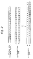
- Figure 1 is a block diagram of a signal transmission system to which the circuit of the present invention is applied; and Fig. 2 is a timing chart showing the data which flows in the system shown in Fig. 1.
- a transmitter device 1 modulates a PAL video signal to a DPCM (differential pulse code modulation) form to prepare a 68-Mb/sec signal, and the 68-Md/sec signal is divided into two low-speed signals A and B through a distribution device 2.
- the signals A and B are transmitted through transmission paths 3 and 4 having a transmission rate of 34.368 Mb/sec rated by the CCITT recommendation, and are mixed by a mixing device 5 to reproduce the 68-Mb/sec signal.
- the reproduced signal is then received by a receiver device 6.
- Fig. 2 (a) is an original data (DPCM signal), (b) is transmitted data having substantially the same phase and transmitted on the transmission lines A and B, and (c) is received data. In this case, a difference of propagation time occurs between the received data A and B.
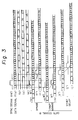
- Figure 3 is a timing chart showing a principle of adjusting the difference of the propagation time between the data A and the data B mentioned above.
- FIG. 3 shows a data signal A
- (b) and (d) are contents of elastic memories storing the content of the data, which is divided into three portions and delayed by one bit of data.
- (e), (g), (i) are the data signal B, wherein (e) is in phase with the data signal A, (g) is advanced to the data signal B by 1.5 bits, and (i) is delay from the data signal B by 1.5 bits.
- the data signal (e), (g) and (i) are delayed by the same bit as (f), (h), (j) in Fig. 3. As shown in Fig.
- the delayed data (f), (h) and (i) are positioned in the range where the corresponding data are stored in the data (b), (c) and (d).
- data "1" in the data signal B are positioned in the range of data "1" in the data signal (b) regardless of when the signal data B is advanced or delayed as shown in (h) or (j).
- Figure 4 shows an arrangement based on the principle of the present invention.
- Reference numerals 101 and 102 denote first and second elastic memories, respectively, and 106, a counter.
- the first and second elastic memories 101, 102 simultaneously receive a first data signal A (shown in Fig. 3 (a)) and a sync signal A (shown in Fig. 3 (a')) synchronous therewith, which have the same bit length, and are operated in response to an output from the counter 106 for counting clocks A synchronous with the data signal A. Then the data (b), (c), (d) shown in Fig. 3 are read out from the elastic memory 101.
- Reference numeral 103 denotes a fixed delay circuit, which delays a second data signal B shown in (e), (g), (i) of Fig. 3 and a sync signal B (shown in Fig. 3 (e'), (g'), (i')) synchronous therewith by the same number of bits.
- Reference numeral 104 denotes a counter, which has the same number of bits as that of the first and second elastic memories 101 and 102 and is operated in response to the clocks B synchronous with the second data signal B.
- the counter 104 loads the position of the first sync signal A shown in Fig. 3 (a') in the elastic memory 102 in response to the delayed second sync signal B (shown in Fig. 3 (f'), (h'), (j')).
- Reference numeral 105 denotes a data selector for sequentially reading out the corresponding data signal A (shown in Fig. 3 (b), (c), (d)) from the first elastic memory 101 in response to the output from the counter 104.
- the data signals A and B are received in phase, in advance phase (for example, 1.5 bit) or delayed phase (for example 1.5 bit).
- the data signal A is divided by the elastic memory 101 into n (for example three) phase signals and accordingly, each phase signal becomes n bits (for example, 3 bits) in width.
- the data selector 105 reads, in order, the output of the elastic memory 101 in accordance with the clock from the counter 104, and the phase of the clock of the counter 104 coincides with the phase of the sync signal B, then the phase of the data signal A from the data selector 105 coincides with the phase of the data signal B from the fixed delay circuit 103.
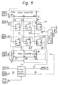
- Figure 5 shows one embodiment of the present invention, in Fig. 5, reference numeral 11 denotes a 3-bit ring counter; and 12, a NAND gate.
- Reference numerals '13, 14, and 15 denote flip-flops (to be referred to as F ⁇ Fs hereinafter), which constitute a 3-bit memory cell, that is, the elastic memory cell 101 shown in Fig. 4.
- Reference numeral 18 denotes a data selector corresponding to 105 in Fig. 4.
- Reference numerals 21, 22, and 23 denote flip-flops (to be referred to as F ⁇ Fs hereinafter), which constitute a 3-bit memory cell that is, the elastic memory cell 102 in Fig. 5.
- Reference numeral 24 (corresponds to 103 in Fig. 4) denotes a fixed delay circuit.
- Figure 5 exemplifies a case wherein one data input B of two data inputs A and B is constantly delayed by 1.5 bits by the fixed delay circuit 24, and the other data input A is variably delayed through a 3-bit elastic memory.
- the sync signals A and B are signals indicating the positions of the phases of the data inputs A and B at the transmission side.
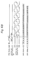
- Figure 6 shows the respective signals in the embodiment shown in Fig. 5.
- Fig. 6 a indicates a write clock A input; b, c, and d, Q1 , Q2 , and Q3 outputs of the 3-bit ring counter 11, respectively; e, a data A input; f, g, and h, Q outputs of the F ⁇ F 13 the F ⁇ F 14, and the F ⁇ F 15, respectively; i , a sync signal B input; j, k, and , Q outputs of the F ⁇ F 21, the F ⁇ F 22, and the F ⁇ F 23, respectively; m, a sync signal B input, n, an output of the fixed delay circuit 24, o, p, and q, Q1 , Q2 , and Q3 outputs of the 3-bit ring counter 16, respectively; r,a data B' output of the fixed delay circuit 24, and s , a data A' output of the data selector 18.
- the ring counter 11 generates three phase clock outputs b, c, and d which sequentially go to "1" level at every leading edge of the write clock A synchronous with the data A input indicated by a from the output terminals Q1 , Q2 , and Q3 thereof.
- the F ⁇ F 13, and F ⁇ F 14, and F ⁇ F 15 constituting the memory cell respectively receive the parallel data A inputs (1, 2, 3, ...) indicated by e at their data terminals D and also receive the clocks b, c, and d at their clock terminals CK.
- the F ⁇ F 13, F ⁇ F 14, and F ⁇ F 15 retrieve the data A inputs in response to the trailing edges of the clocks b, c, and d, thus generating the outputs f (1, 4, %), g (2, 5, %) and h (3, 6, 7) from their Q outputs.
- the F ⁇ F 21, F ⁇ F 22, and F ⁇ F 23 respectively receive the parallel sync signal A input indicated by i at their data terminals D and the clocks b, c, and d at their clock terminals CK, and retrieve the sync signal A in response to the leading edges thereof.
- the sync signal A is synchronous with a signal (1) in the data A input.
- the F ⁇ F 21 loads a "1" in response to the trailing edge of the clock b, and holds a "1" at its output j during a 3-bit interval until the clock c trails again.
- the outputs k and l are at "0" level.
- the data B input and the sync signal B input indicated by m are delayed by 1.5 bits by the fixed delay circuit 24, thus producing the data B output and the sync signal output n.
- the 3-bit ring counter 16 receives the sync signal output n at its load terminal LOAD. When the signal n is at "1" level, the counter 16 loads the values of the outputs j, k, and applied to its data terminals D1 , D2 , and D3 in response to the leading edge of the read clock B input, thereby producing the outputs o, p, and q, respectively. In this case, the output o, is at "1" level, and the outputs p and q are at "0" level.
- the data selector 18 selects and outputs the data f of the corresponding F ⁇ F 13, thereby producing data of (1) from the data A' output.
- the 3-bit ring counter 16 receives the read clock B input at its clock terminal CK, and generates the outputs o, p, and q from the terminals Q1 , Q2 , and Q3 which subsequentially go to "1" level, respectively.
- the data selector 18 sequentially selects and outputs the data f, g, and h.
- data of (2), (3), (4), ... are sequentially selected and are output to the data A output indicated by s.
- the data A is phase-locked with the sync signal B (n) passing through the fixed delay circuit 24 and is output to the output s via the data selector 18, thereby adjusting the phase difference between the data A and B.
- Fig. 5 when the data A input has the phase difference falling within the range of ⁇ 1.5 bits compared to the data B input, this difference can be adjusted to lock their phases.
- Fig. 6B indicates a case wherein the date B input advances from the data A input by 1.5 bits, and indicates a case wherein the data B input is delayed from the data B input by 1.5 bits.
- the sync signal B (n) passing through the fixed delay circuit 24 also advances or is delayed by 1.5 bits
- the data A output indicated by s also advances or is delayed by the same number of bits. Therefore, the phase adjustment with respect to the data A output can be similarly performed.
- Figure 7 shows a practical application of the method of the present invention to an apparatus.
- Figure 7 exemplifies a case wherein the phases of inputs 1 and 2 of third multiplexed data D3, which have the phase difference of ⁇ D bits, are adjusted.
- a first input D3 IN1 consisting of a bipolar signal is converted to a unipolar signal by a bipolar/unipolar converter (B/U) 31, and a high density bipolar (HDB3) code is decoded by an HDB3 decoder (HDB/3/U) 32, thus producing a 34 MHz clock signal as well as a 34-Mb/sec data signal.
- B/U bipolar/unipolar converter
- HDB3 decoder HDB/3/U
- a demultiplexer (DMUX) 33 demultiplexes these signals and produces eight 4-Mb/sec data signals, a 4 MHz clock signal, and a frame signal.
- the eight data signals and the frame signal are delayed through nine D/8-bit delay circuits in a fixed delay circuit 34, and the data signal is output as output data DATA OUT1.
- a second data input D3 IN2 similarly passes through a bipolar/unipolar converter (B/U) 35, and HDB3 decoder (HDB3/U) 36, and a demultiplexer (DMUX) 37, thus producing eight 4-Mb/sec data signals, a 4 MHz clock signal, and a frame signal.
- the eight data signals and the frame signal are input to a variable delay circuit 38, and are delayed through nine D/4-bit delay circuits.
- variable delay circuit 38 uses the 4 MHz clock signal from the DMUX 37 as a write clock, the 4 MHz clock signal from the DMUX 33 as a read clock, and the frame signal passing through the fixed delay circuit 34 as a delayed sync signal, and is operated in the same manner as in the embodiment shown in Fig. 5, thereby producing output data DATA OUT2 which is phase-locked with the output data DATA OUT1.
- one signal is applied to an elastic memory to read out data therefrom and obtain an output in response to a ring counter output which is stepped by the number of bits corresponding to a difference between delay times of the sync signals of two signals, and the other signal is constantly delayed by a given number of bits. Therefore, even if one signal is either advanced or delayed from the other signal, any difference in the delay times can be absorbed.
Landscapes
- Engineering & Computer Science (AREA)
- Computer Networks & Wireless Communication (AREA)
- Signal Processing (AREA)
- Computer Hardware Design (AREA)
- Power Engineering (AREA)
- Synchronisation In Digital Transmission Systems (AREA)
- Time-Division Multiplex Systems (AREA)
- Dc Digital Transmission (AREA)
Applications Claiming Priority (2)
| Application Number | Priority Date | Filing Date | Title |
|---|---|---|---|
| JP60195623A JPS6256040A (ja) | 1985-09-04 | 1985-09-04 | 遅延時間補償回路 |
| JP195623/85 | 1985-09-04 |
Publications (3)
| Publication Number | Publication Date |
|---|---|
| EP0213641A2 EP0213641A2 (en) | 1987-03-11 |
| EP0213641A3 EP0213641A3 (en) | 1989-05-03 |
| EP0213641B1 true EP0213641B1 (en) | 1993-05-12 |
Family
ID=16344247
Family Applications (1)
| Application Number | Title | Priority Date | Filing Date |
|---|---|---|---|
| EP19860112327 Expired - Lifetime EP0213641B1 (en) | 1985-09-04 | 1986-09-04 | Delay time adjusting method, circuit, and system |
Country Status (3)
| Country | Link |
|---|---|
| EP (1) | EP0213641B1 (enExample) |
| JP (1) | JPS6256040A (enExample) |
| DE (1) | DE3688410T2 (enExample) |
Families Citing this family (13)
| Publication number | Priority date | Publication date | Assignee | Title |
|---|---|---|---|---|
| US4979190A (en) * | 1988-04-01 | 1990-12-18 | Digital Equipment Corporation | Method and apparatus for stabilized data transmission |
| US4811364A (en) * | 1988-04-01 | 1989-03-07 | Digital Equipment Corporation | Method and apparatus for stabilized data transmission |
| JPH0435394A (ja) * | 1990-05-28 | 1992-02-06 | Fujitsu Ltd | 高品位テレビ信号符号化装置 |
| JP2816384B2 (ja) * | 1990-06-14 | 1998-10-27 | 富士通株式会社 | 位相補正方法及び回路 |
| US5119402A (en) * | 1990-06-26 | 1992-06-02 | Digital Equipment Corporation | Method and apparatus for transmission of local area network signals over unshielded twisted pairs |
| US5341405A (en) * | 1991-06-11 | 1994-08-23 | Digital Equipment Corporation | Data recovery apparatus and methods |
| US5408473A (en) * | 1992-03-03 | 1995-04-18 | Digital Equipment Corporation | Method and apparatus for transmission of communication signals over two parallel channels |
| EP0651927B1 (de) * | 1992-07-20 | 1996-10-09 | Siemens Aktiengesellschaft | Verfahren zur weiterleitung eines nachrichtenzellenstroms über eine mehrzahl paralleler verbindungsleitungen unter einhaltung der reihenfolge der nachrichtenzellen |
| US5359630A (en) * | 1992-08-13 | 1994-10-25 | Digital Equipment Corporation | Method and apparatus for realignment of synchronous data |
| US6336192B1 (en) * | 1998-02-16 | 2002-01-01 | Nippon Telegraph And Telephone Corporation | Parallel redundancy encoding apparatus |
| EP0996262A1 (en) * | 1998-10-22 | 2000-04-26 | Texas Instruments France | Communication system with plurality of synchronised data links |
| US6963989B1 (en) * | 2000-05-22 | 2005-11-08 | Micron Technology, Inc. | Method and apparatus for adjusting data hold timing of an output circuit |
| US7035368B2 (en) | 2002-03-18 | 2006-04-25 | Texas Instruments Incorporated | High speed parallel link receiver |
Family Cites Families (1)
| Publication number | Priority date | Publication date | Assignee | Title |
|---|---|---|---|---|
| GB968730A (enExample) * | 1962-02-09 |
-
1985
- 1985-09-04 JP JP60195623A patent/JPS6256040A/ja active Granted
-
1986
- 1986-09-04 EP EP19860112327 patent/EP0213641B1/en not_active Expired - Lifetime
- 1986-09-04 DE DE19863688410 patent/DE3688410T2/de not_active Expired - Fee Related
Also Published As
| Publication number | Publication date |
|---|---|
| JPH035100B2 (enExample) | 1991-01-24 |
| DE3688410T2 (de) | 1993-11-11 |
| EP0213641A2 (en) | 1987-03-11 |
| JPS6256040A (ja) | 1987-03-11 |
| DE3688410D1 (de) | 1993-06-17 |
| EP0213641A3 (en) | 1989-05-03 |
Similar Documents
| Publication | Publication Date | Title |
|---|---|---|
| EP0213641B1 (en) | Delay time adjusting method, circuit, and system | |
| GB2210231A (en) | Synchroniser for television audio and video signals | |
| US5398241A (en) | High speed asynchronous multiplexer demultiplexer | |
| EP0249985B1 (en) | Video memory | |
| JP2010110012A (ja) | オーディオ/ビデオ/データをシステム・バスを介して転送する方法 | |
| JPH04211534A (ja) | データ伝送方法 | |
| US5014271A (en) | Pulse insertion circuit | |
| EP0201971A2 (en) | Communication system | |
| US4731646A (en) | Moving-image coder with self-identification of the stuffing characters | |
| US5654967A (en) | Delay-in-frames correcting system in a PCM transmission line | |
| JPH05199199A (ja) | スタッフ同期制御方式 | |
| JPH0225576B2 (enExample) | ||
| JP2851045B2 (ja) | 映像デジタル伝送方式とその受信装置 | |
| US5781587A (en) | Clock extraction circuit | |
| DE60122841T2 (de) | Synchrones Datenübertragungssystem | |
| US5165092A (en) | Method of processing the signalling information within configurable multiplexers | |
| CA2112059A1 (en) | Hdtv signal transmission apparatus | |
| JP2605435B2 (ja) | Pcm伝送装置とpcm受信装置およびディジタル・オーディオ・インターフェース・フォーマット・データ伝送装置とディジタル・オーディオ・インターフェース・フォーマット・データ受信装置 | |
| JPS5811781B2 (ja) | タジユウデイジタルカイセンモウノ ケツゴウブンキソウチ | |
| JPH0756962B2 (ja) | データ通信システム | |
| JPH03173233A (ja) | ジッタ低減方式 | |
| JP2697629B2 (ja) | 速度変換装置 | |
| Kansal et al. | Enhanced satellite bandwidth utilization by optimum integration of split trunks and transcoders | |
| JPH0666739B2 (ja) | 分離回路 | |
| JPH0250662B2 (enExample) |
Legal Events
| Date | Code | Title | Description |
|---|---|---|---|
| PUAI | Public reference made under article 153(3) epc to a published international application that has entered the european phase |
Free format text: ORIGINAL CODE: 0009012 |
|
| AK | Designated contracting states |
Kind code of ref document: A2 Designated state(s): DE FR GB |
|
| PUAL | Search report despatched |
Free format text: ORIGINAL CODE: 0009013 |
|
| RHK1 | Main classification (correction) |
Ipc: H04J 3/06 |
|
| AK | Designated contracting states |
Kind code of ref document: A3 Designated state(s): DE FR GB |
|
| 17P | Request for examination filed |
Effective date: 19890530 |
|
| 17Q | First examination report despatched |
Effective date: 19920130 |
|
| GRAA | (expected) grant |
Free format text: ORIGINAL CODE: 0009210 |
|
| AK | Designated contracting states |
Kind code of ref document: B1 Designated state(s): DE FR GB |
|
| REF | Corresponds to: |
Ref document number: 3688410 Country of ref document: DE Date of ref document: 19930617 |
|
| ET | Fr: translation filed | ||
| PGFP | Annual fee paid to national office [announced via postgrant information from national office to epo] |
Ref country code: GB Payment date: 19950824 Year of fee payment: 10 |
|
| PGFP | Annual fee paid to national office [announced via postgrant information from national office to epo] |
Ref country code: FR Payment date: 19950911 Year of fee payment: 10 |
|
| PGFP | Annual fee paid to national office [announced via postgrant information from national office to epo] |
Ref country code: DE Payment date: 19950918 Year of fee payment: 10 |
|
| PG25 | Lapsed in a contracting state [announced via postgrant information from national office to epo] |
Ref country code: GB Effective date: 19960904 |
|
| PG25 | Lapsed in a contracting state [announced via postgrant information from national office to epo] |
Ref country code: FR Effective date: 19960930 |
|
| GBPC | Gb: european patent ceased through non-payment of renewal fee |
Effective date: 19960904 |
|
| PG25 | Lapsed in a contracting state [announced via postgrant information from national office to epo] |
Ref country code: DE Effective date: 19970603 |
|
| REG | Reference to a national code |
Ref country code: FR Ref legal event code: ST |
|
| REG | Reference to a national code |
Ref country code: FR Ref legal event code: ST |
|
| PLBE | No opposition filed within time limit |
Free format text: ORIGINAL CODE: 0009261 |
|
| STAA | Information on the status of an ep patent application or granted ep patent |
Free format text: STATUS: NO OPPOSITION FILED WITHIN TIME LIMIT |