EP0211232B1 - Halbleiterspeicher mit einem Leseverfahren in einem grossen Speisespannungsbereich - Google Patents
Halbleiterspeicher mit einem Leseverfahren in einem grossen Speisespannungsbereich Download PDFInfo
- Publication number
- EP0211232B1 EP0211232B1 EP86108940A EP86108940A EP0211232B1 EP 0211232 B1 EP0211232 B1 EP 0211232B1 EP 86108940 A EP86108940 A EP 86108940A EP 86108940 A EP86108940 A EP 86108940A EP 0211232 B1 EP0211232 B1 EP 0211232B1
- Authority
- EP
- European Patent Office
- Prior art keywords
- voltage
- word line
- level
- memory cell
- signal
- Prior art date
- Legal status (The legal status is an assumption and is not a legal conclusion. Google has not performed a legal analysis and makes no representation as to the accuracy of the status listed.)
- Expired - Lifetime
Links
Images


Classifications
-
- G—PHYSICS
- G11—INFORMATION STORAGE
- G11C—STATIC STORES
- G11C8/00—Arrangements for selecting an address in a digital store
- G11C8/08—Word line control circuits, e.g. drivers, boosters, pull-up circuits, pull-down circuits, precharging circuits, for word lines
-
- G—PHYSICS
- G11—INFORMATION STORAGE
- G11C—STATIC STORES
- G11C16/00—Erasable programmable read-only memories
- G11C16/02—Erasable programmable read-only memories electrically programmable
- G11C16/06—Auxiliary circuits, e.g. for writing into memory
- G11C16/08—Address circuits; Decoders; Word-line control circuits
Definitions
- the present invention relates to a semiconductor memory and, more particularly, to a driving of word lines in a programmable read-only memory (referred hereinafter to as a "PROM") having memory cells each constituted with a field effect transistor having a floating gate.
- PROM programmable read-only memory
- a data readout operation is performed by using a difference in threshold voltage between a programmed memory cell and a non-programmed memory cell.
- the floating gate of the programmed memory cell is charged negative or positive due to electrons or holes injected therein, and therefore, the threshold value thereof takes a high value V TMW .
- the threshold value takes a low value V TMO .
- Each memory cell is applied with a voltage between V TMW and V TMO as a readout voltage. Therefore, the non-programmed memory cell is turned on while the programmed memory cell is kept non-conductive. Thus, an output data is obtained as "1" or "0" dependent upon whether or not the selected memory cell is programmed.
- the readout voltage is reduced with a drop of a power supply voltage.
- the readout voltage becomes smaller than the low threshold voltage V TMO due to the drop of the power voltage, all of the memory cells are kept non-conductive regardless of whether or not they are programmed.
- the low threshold value V TMO of an N channel non-programmed memory cell is about 2.5 V, and a readout voltage of at least 3 V is required in order to make the memory cell conductive realiably. Therefore, when the readout voltage is lowered below 3 V due to the power voltage drop, the data readout from the EPROM becomes impossible.
- a semiconductor memory according to the preamble of claim 1 is disclosed in GB-A-2 144 006.
- this memory distributors and a voltage step-up circuit which operate only a data write mode, are provided to supply a selected word line with a programming voltage higher than a predetermined programming voltage to shorten the data write operation, i.e. the programming operation.
- a predetermined programming voltage i.e. the programming operation.
- a fixed read-out voltage is supplied to the selected word line, so that the problems as indicated above are also present in this memory.
- EP-A-106 222 is related to the problem of providing a static type memory free from soft errors caused by alpha particles in a battery back-up mode. For this purpose the power supply voltage is boosted and supplied to power terminals of the memory cells.
- the voltage of the selected word line is raised in the reading operation relative to a power supply voltage.
- This can be achieved by utilizing a capacitive element which is connected to the selected word line and which is first charged up to the selection level of the word line. Thereafter, a voltage higher than the non-selection level is applied to the other end of the capacitive element.
- the potential on the selected word line is raised by the bootstrap effect of the capacitive element.
- a voltage which is higher than the prior art readout voltage is applied to the selected memory cell as an actual readout voltage.
- the readout operation is performed even when the source voltage drops.
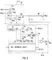
- Fig. 1 shows a block diagram of a PROM according to an embodiment of the present invention.
- a plurality of memory cells MC11 to MC mn are arranged in n lines and m rows to constitute a memory cell array 1.
- Each memory cell is constituted with an N channel field effect transistor having a control gate CG, a floating gate FG and a source-drain current path.
- the control gate CG of each memory cell is connected to one of word lines Wo to Wm and the source-drain path thereof is connected between one of digit lines D1 to Dn and a ground point.
- N channel gate transistors MG1 to MGn are connected, respectively.
- Row address signals RAo to RAi are supplied through row address terminals 11-0 to 11-i to a row address buffer 3. Signals RAoo to RAii from the buffer 3 are supplied to a row address decoder 2. The decoder 2 thereby changes one of selection signals Xo to Xm to a selection level and energizes an associated word line W.
- Column address signals CAo to CAj are supplied via column address terminals 12-o to 12-i to a column address buffer 5.
- a column address decoder 4 responds to the outputs CAoo to CAjj of the buffer 5 and raises one of decoded signals Yo to Yn to the high level, so that an associated gate transistor MG is turned on. As a result, one memory cell MC is selected.
- a signal WE supplied to a terminal 13 is used to bring the PROM into a data readout operation or a data programming operation.
- a read/write control circuit 6 changes a read-enable signal RE to the high level and a write-enable signal WE to the low level. Therefore, the sense amplifier 7 is activated to amplify a data in the selected memory cell and provides the amplified data at a terminal 14 as an output data Dout.
- the write-enable signal WE becomes the high level and a data programming operation is performed. At this time, a programming voltage Vpp is supplied to a terminal 15.
- a programming circuit 9 responds to an output produced by a data input circuit 8 according to an input data D IN supplied to the terminal 14 and controls whether or not the programming voltage Vpp is applied to the selected word line W and the selected digit line D.
- Vpp programming voltage
- the selected memory cell is supplied with the voltage Vpp at its control gate CG and across its the source-drain current, electrons are injected into its floating gate FG.
- the gate FG is thereby charged negative.
- the threshold value thereof becomes high, and a programmed memory cell is thus formed.
- Fig. 6 shows control gate voltage V CG versus drain-source current I DS characteristics curves 60 and 50 of a programmed memory cell and a non-programmed memory cell, respectively.
- the floating gate thereof is not charged negative. Therefore, its threshold value V TMO is about 2.5 V and it is turned on by a control gate voltage V CG exceeding the threshold value, so that a drain current I DS increases.
- the programmed memory cell has a threshold value T TMW of about 13 V since its floating gate is charged negative. Therefore, the programmed memory cell is not turned on so long as its control gate voltage V CG does not exceed the threshold value V TMW .
- an intermediate voltage between the threshold values V TMO and V TMW is thus applied to the control gate CG of the selected memory cell MC as a readout voltage.
- the row address decoder 2 responds to the row address signals RAo to RAi and changes one of the selection signals Xo to Xm to this intermediate voltage to energize the associated word line W.
- the power voltage Vcc applied to a power supply terminal 16 is 5 V, and thus used as that intermediate voltage, advantageously.
- PROMs have been employed in various equipments powered by batteries. Electromotive force of a battery reduces with its use. This means that the readout voltage to be supplied to the memory cell drops gradually.
- the threshold value V TMO of the non-programmed memory cell is about 2.5 V, but a control gate voltage V CG of at least 3 V is required in order that the non-programmed memory cell produces a readout current I D .
- the sense amplifier will judge the non-programmed memory cell as a programmed memory cell. That is, the data readout operation becomes impossible.
- the PROM shown in Fig. 1 further includes a signal generator 10 generating word line pull-up signals RSo to RSm in response to a potential change in the outputs RAoo to RAii of the row address buffer 3 (i.e., potential change in the row address signals RAo to RAi), and capacitors Co to Cm connected, respectively, between output out terminals of the signal generator 10 and the word lines Wo to Wm.
- the pull-up signals RSo to RSm are generated after the row address decoder 2 raises the selected signal X to the selection level.
- the capacitor C connected to the energized word line is first charged to the selection level and thereafter supplied with the pull-up signal RS. Accordingly, the word line W is further charged up to a level of a sum of the selection level of the signal X and the signal level of the signal RS.
- the non-programmed memory cell receives at its control gate a voltage V CG that is enough to produce the readout current I R even when the power voltage V CC drops below 3 V (Fig. 6).
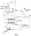
- Fig. 2 is a circuit diagram of a row address decoder 2-0 and a word line pull-up signal generator 10-0 both associated with the word line Wo.
- the decoder 2-0 includes P-channel transistors M20 and M21 and N-channel transistors M22, and M23, these transistors constituting a NOR circuit having 2 inputs to which the signals RA oo and RA11 are supplied from the address buffer 3. When both of the signals RA00 and RA11 are in the low level, an output of the NOR circuit becomes the high level.
- the output of the NOR circuit is supplied through an N-channel depletion type transistor M24 to the word line Wo as a selection signal Xo.
- the read-enable signal RE is supplied to the gate of the transistor M24.
- the signal generator 10-0 generating the word line pull-up signal RSo includes an RA00 responsive circuit 10-0-1 and an RA11 responsive circuit 10-0-2. Since these responsive circuits have the same construction, only the circuit 10-0-1 is shown in detail in Fig. 2.
- the signal RA00 is delayed by a delay circuit 20 to provide a delayed signal V20.
- the delay circuit 20 may be constructed with a plurality of inverters connected in series.
- the signal V20 is supplied through an N-channel transistor M25 having a gate supplied with the power voltage V CC to an inverter 21 whose output is in turn supplied to an inverter 22.
- An inverted signal V22 from the inverter 22 is supplied through an N-channel transistor M26 having a gate supplied with the power voltage V CC to an inverter 23.
- the outputs V21 and V23 of the inverters 21 and 23 are supplied to gates of N-channel transistors M27 and M28, respectively.
- Source-drain current paths of the transistors M27 and M28 are connected between the output terminal of the delay circuit 20 and a node N1 and between the output terminal of the inverter 22 and the node N1, respectively.
- a signal appearing at the node N1 is derived as an output of the circuit 10-0-1 and, together with an output of the RA11 responsive circuit 10-0-2, supplied to an NOR circuit 24.
- An output of the NOR circuit 24 is supplied to an inverter 25 whose output is derived as the pull-up signal RSo of the generator 10-0.
- a capacitor Co is connected between the output terminal of the signal generator 10-0 and the word line Wo.
- Fig. 3 shows a timing chart representative of the circuit operation.
- the row address decoder 2 does not energize the word line Wo and does another word line. Therefore, the signals, RA00 and RA11 takes the high level and the low level, respectively, for example.
- the signal RA11 is kept the low level according to the previous address information. Consequently, the transistors M20 and M21 are turned on and the transistors M22 and M23 are turned off. The potential at a node N2 is thus raised the power voltage V cc (high level).
- the selection signal Xo takes the selection level and the word line Wo is energized to be charged.
- the potential Vr of the word line Wo takes a V xo level.
- the level V xo is slightly lower than the power voltage V CC as shown in Fig. 3 due to the existence of the transistor M24.
- the level change of the signal RA00 is supplied to the circuit 10-0-1 and delayed by the delay circuit 20.
- the delayed output V20 of the delay circuit 20 is changed to the low level at a time point T2.
- the delay time of the circuit 20 is selected to be longer than a time required for charging the word line Wo to the level V xo .
- the output signal V22 of the inverter 22 is changed to the high level.
- the transistor 26 acts as a delay element.
- the gate of the transistor M28 is in the high level at the time point T2.
- the node N1 is thereby changed to the high level.
- the output of the inverter 25 (therefore, the signal RSo) takes the power voltage V CC (high level). Since the capacitor Co is charged to the level V xo for a time from the time instance T1 to the time instance T2, the potential Vr of the word line Wo is pulled up by the high level signal RSo supplied to the capacitor Co and thus takes a (V xo + V CC ) level as shown in Fig. 3.
- This potential level is supplied to the control gates CG of the memory cells MC11 to MCln (Fig. 1) as a readout voltage.
- a memory cell MC11 is selected. Further assuming that the memory cell MC11 is a non-programmed cell, this cell is turned on to produce the readout current I D . As as result, the sense amplifier 7 produces an output data Dout of "0", for example. If the cell MC11 is programmed, its threshold value V TMW is about 13 V. On the other hand, the readout voltage level (V xo + V CC ) is lower than 10 V. Therefore, the cell MC11 is maintained in the non-conductive state and the sense amplifier 7 produces an output data Dout of "1".
- the N-channel depletion transistor M24 has a negative threshold value.
- the node N2 to which one of the drain and source of the transistor M24 is connected takes the power voltage V CC
- the word line Wo to which the other of them is connected takes the (V xo + V CC ) level.
- the back gate biasing-effect occurs to shift the threshold value of the transistor M24 to a positive value.
- the signal RE i.e. the gate of the transistor M24, takes the power voltage V CC (high level), and the source and drain thereof take a potential that is equal to or higher than the gate potential. Therefore, the transistor M24 is turned off when the potential of the word line Wo exceeds the power voltage V CC .
- the word line Wo and the decoder circuit 2-0 are thereby separated from each other.
- the outputs V21 and V23 of the inverters 21 and 23 are inverted respectively to the high level and the low level at a time point 3.
- Transistors M27 and M28 are thereby turned on and off, respectively.
- the signal V20 is in the low level at the time point T3. Therefore, the node N1 is discharged to the low level and the signal RSo is inverted to the low level.
- the potential Vr of the word line Wo is thereby discharged to the V xo level. As a result, the data readout operation responsive to the change in the address signals is completed.
- the readout voltage which is actually supplied to the selected memory cell MC takes the level which is approximately as high as twice the power voltage V CC . Therefore, the non-programmed cell receives the control gate voltage V CG which is required for obtaining the readout current I D even when the power voltage V CC is lowered to about 1.5 V.
- the range of the power voltage within which the data readout operation is carried out is expanded in the PROM shown in Figs. 1 and 2.
- the transistors M20 and M23 are turned off and on, respectively, so that the word line Wo is discharged to the ground level (low level).
- the signal generator 10-0 responds to the change in the address signals and produces again the high level pull-up signal RSo at a time point T5, but at this time, the transistor M23 clamps the word line Wo at the ground level. Therefore, a substantial level increase does not occure on the word line Wo.
- the readout voltage taking the (V xo + V CC ) level is supplied to a newly selected memory cell by the operations of the signal generator 10 and other capacitors C shown in Fig. 1.
- Fig. 4 shows another embodiment of the present invention, in which only portions corresponding to those shown in Fig. 2 are shown.
- the same constituents as those shown in Fig. 2 are depicted by the same reference numerals and symbols to omit their further description.
- a readout voltage V R higher than V CC is applied to a selected memory cell only when the source voltage V CC is lower than a predetermined value, and that means is provided for reliably separating the row decoder circuit from the boosted word line.
- a comparator 32 is used to detect the power voltage V CC .
- the non-inverted input terminal(+) of the comparator 32 is supplied with the power voltage V CC and the inverted input terminal(-) thereof is supplied with a reference voltage Vref from a reference voltage source 33.
- the reference voltage Vref is selected to be a voltage value by which the non-programmed memory cell produces the readout current I R , i.e., 3 V (refer to Fig. 6).
- the output V D of the comparator 32 is supplied to one input terminal of an NOR circuit 30 which has the other input terminal supplied with an output RSo' of an NOR circuit 24.
- the output of the NOR circuit 30 is supplied to the capacitor Co as the pull-up signal RSo and further to an inverter 31.
- the output of the inverter 31 is supplied to the gate of a transistor M24 as a gate control signal GC.
- the output V D of the comparator 32 takes the high level, as shown in Fig. 5A. Therefore, the signal RSo is clamped to the low level regardless of the level change in the signal RAoo or RA11 caused by the change in the address signals. The signal GC takes therefore the high level. Consequently, the voltage V R of the word line Wo takes the Vxo level and is supplied to the memory cell MC11 as a readout voltage.
- the comparator 32 When the source voltage V CC is reduced to a level V CC1 that is lower than the reference voltage Vref, the comparator 32 produces a low level output V D as shown in Fig. 5B.
- the signal RA11 is changed to the low level due to the change in the address signal (the signal RAoo is in low level)
- the transistors M20 and M21 are turned on to charge the word line Wo to the Vxo level.
- the output RSo' of the NOR circuit 24 is inverted to the low level and the signal RSo is inverted to the high level after the capacitor Co is charged to the Vox level.
- the word line is further charged, so that its potential V R takes the (Vxo + V CC1 ) level.
- the signal RSo Since the signal RSo is in high level, the signal CG, i.e. the gate of the transistor M24, takes the low level. Thus, the gate of the transistor M24 takes the low level while both of the source and drain thereof are takes the level higher than the level at the gate. Therefore, the transistor M24 is ensured to be the non-conductive state even if the threshold value thereof has deviation from a designed value.
- the decoder circuit 2-0 is thereby separated completely from the word line Wo. When the signal RSo is inverted to the low level, the potential V R of the word line is decreased to the Vxo level.
- the range of the source voltage within which the data readout operation is carried out is also expanded in this embodiment. Furthermore, since the bootstrap effect of the word line potential is performed only when the power voltage is lowered, the problem that the programmed memory cell may be turned on when the power voltage V CC is increased, is resolved, which may otherwise occur in the memory shown in Figs. 1 and 2.
- the transistor M24 shows in Fig. 2 can be supplied at its gate with the low level at the boosting time of the word line in accordance with the teaching of Fig. 4.
- the signal generators 10-0-1 and 10-0-2 shown in Figs. 2 and 4 may respond only to a change in the signals RAoo and RA11 from the high level to the low level and produce the high level signal.
- the respective embodiments described hereinbefore are constituted with complementary insulated-gate field effect transistors, they may be constituted only with N channel transistors or P channel transistors.
Claims (1)
- Halbleiterspeicher mit einem Speicherzellenfeld (1) mit einer Vielzahl von Speicherzellen (MC), einer Anzahl von Wortleitungen (WO-Wm) und einer Anzahl von Zahlenleitungen (D1-Dn), wobei jede der Speicherzellen einen Feldeffekttransistor mit einem Floating-Gate (FG), ein Steuergate (CG), das mit einer der Wortleitungen (W) verbunden ist, und einen Source-Drain-Weg aufweist, der mit einer der Zahlenleitungen (D) verbunden ist, wobei der Feldeffekttransistor eine erste Schwellspannung (VTMO) aufweist, die in einem nichtprogrammierten Zustand geringer ist als die Versorgungsspannung (Vcc), und eine zweite Schwellspannung (VTMW), die in einem programmierten Zustand größer ist als die Versorgungsspannung (Vcc), und mit einer Einrichtung (2-5 MG), die auf einen Satz von Adressignalen (RA, CA) anspricht, zur Auswahl von zumindest einer Wortleitung (W) und zumindest einer Zahlenleitung (D) zur Bezeichnung zumindest einer der Speicherzellen (MC), wobei die Auswahleinrichtung ferner eine Einrichtung (2, 3) aufweist zur Versorgung der ausgewählten Wortleitung mit einer Auslesespannung (Vxo) zwischen dem ersten Schwellwert (VMTO) und der Versorgungsspannung (Vcc) zur Auswahl von Daten aus der bezeichneten Speicherzelle,
gekennzeichnet durch ferner eine Einrichtung (10, CO-Cm) zur Versorgung der ausgewählten Wortleitung, nachdem die ausgewählte Wortleitung mit der Auslesespannung (Vxo) geladen ist, mit einer derartigen Zusatzspannung (Vcc), die die Spannung der ausgewählten Wortleitung auf einen Pegel (Vxo + Vcc) oberhalb der Versorungsspannung (Vcc), aber unterhalb der zweiten Schwellspannung (VTMW) anhebt, wobei die Zusatzspannung gleich der Versorgungsspannung ist.
Applications Claiming Priority (4)
| Application Number | Priority Date | Filing Date | Title |
|---|---|---|---|
| JP14503085 | 1985-07-01 | ||
| JP145030/85 | 1985-07-01 | ||
| JP15039685 | 1985-07-08 | ||
| JP150396/85 | 1985-07-08 |
Publications (3)
| Publication Number | Publication Date |
|---|---|
| EP0211232A2 EP0211232A2 (de) | 1987-02-25 |
| EP0211232A3 EP0211232A3 (en) | 1988-12-14 |
| EP0211232B1 true EP0211232B1 (de) | 1993-12-29 |
Family
ID=26476289
Family Applications (1)
| Application Number | Title | Priority Date | Filing Date |
|---|---|---|---|
| EP86108940A Expired - Lifetime EP0211232B1 (de) | 1985-07-01 | 1986-07-01 | Halbleiterspeicher mit einem Leseverfahren in einem grossen Speisespannungsbereich |
Country Status (4)
| Country | Link |
|---|---|
| US (1) | US4811292A (de) |
| EP (1) | EP0211232B1 (de) |
| JP (1) | JP2530821B2 (de) |
| DE (1) | DE3689450T2 (de) |
Families Citing this family (23)
| Publication number | Priority date | Publication date | Assignee | Title |
|---|---|---|---|---|
| US6545913B2 (en) | 1987-06-29 | 2003-04-08 | Kabushiki Kaisha Toshiba | Memory cell of nonvolatile semiconductor memory device |
| US5877981A (en) * | 1987-06-29 | 1999-03-02 | Kabushiki Kaisha Toshiba | Nonvolatile semiconductor memory device having a matrix of memory cells |
| US6034899A (en) * | 1987-06-29 | 2000-03-07 | Kabushiki Kaisha Toshiba | Memory cell of nonvolatile semiconductor memory device |
| US5448517A (en) * | 1987-06-29 | 1995-09-05 | Kabushiki Kaisha Toshiba | Electrically programmable nonvolatile semiconductor memory device with NAND cell structure |
| JPH0766675B2 (ja) * | 1987-07-14 | 1995-07-19 | 株式会社東芝 | プログラマブルrom |
| JPS6432494A (en) * | 1987-07-27 | 1989-02-02 | Mitsubishi Electric Corp | Non-volatile semiconductor storage device |
| JPS6437797A (en) * | 1987-08-03 | 1989-02-08 | Oki Electric Ind Co Ltd | Eprom device |
| JPH023187A (ja) * | 1988-06-09 | 1990-01-08 | Toshiba Corp | 不揮発性半導体メモリ |
| GB2219901B (en) * | 1988-06-17 | 1992-10-07 | Motorola Inc | Eprom programming |
| JP2655441B2 (ja) * | 1990-07-13 | 1997-09-17 | 日本電気株式会社 | 読み出し専用半導体記憶装置 |
| JPH05128866A (ja) * | 1991-10-31 | 1993-05-25 | Toshiba Corp | ランダムアクセスメモリの書き込み、読出し制御回路 |
| DE4493150T1 (de) * | 1993-05-11 | 1995-07-20 | Nippon Kokan Kk | Nichtflüchtige Speichervorrichtung, nichtflüchtige Speicherzelle und Verfahren zum Einstellen des Schwellenwertes der nichtflüchtigen Speicherzelle und jedes der vielen Transistoren |
| JPH0798985A (ja) * | 1993-09-29 | 1995-04-11 | Nec Corp | 半導体記憶回路 |
| US5602779A (en) * | 1994-11-11 | 1997-02-11 | Nkk Corporation | Nonvolatile multivalue memory |
| US5808338A (en) * | 1994-11-11 | 1998-09-15 | Nkk Corporation | Nonvolatile semiconductor memory |
| US5661686A (en) * | 1994-11-11 | 1997-08-26 | Nkk Corporation | Nonvolatile semiconductor memory |
| US5615146A (en) * | 1994-11-11 | 1997-03-25 | Nkk Corporation | Nonvolatile memory with write data latch |
| JPH08329691A (ja) * | 1995-05-30 | 1996-12-13 | Nkk Corp | 不揮発性半導体記憶装置 |
| JPH0945094A (ja) * | 1995-07-31 | 1997-02-14 | Nkk Corp | 不揮発性半導体記憶装置 |
| JPH0945090A (ja) * | 1995-07-31 | 1997-02-14 | Nkk Corp | 不揮発性半導体記憶装置 |
| US6122205A (en) * | 1998-01-28 | 2000-09-19 | Microchip Technology Incorporated | Voltage regulator and boosting circuit for reading a memory cell at low voltage levels |
| US6069825A (en) * | 1998-09-16 | 2000-05-30 | Turbo Ic, Inc. | Charge pump for word lines in programmable semiconductor memory array |
| JP2003052282A (ja) | 2001-08-09 | 2003-02-25 | Johshuya Co Ltd | 魚釣用スピニングリール |
Citations (1)
| Publication number | Priority date | Publication date | Assignee | Title |
|---|---|---|---|---|
| EP0106222A2 (de) * | 1982-10-12 | 1984-04-25 | Kabushiki Kaisha Toshiba | Halbleiterspeicheranordnung |
Family Cites Families (10)
| Publication number | Priority date | Publication date | Assignee | Title |
|---|---|---|---|---|
| US4094012A (en) * | 1976-10-01 | 1978-06-06 | Intel Corporation | Electrically programmable MOS read-only memory with isolated decoders |
| US4340943A (en) * | 1979-05-31 | 1982-07-20 | Tokyo Shibaura Denki Kabushiki Kaisha | Memory device utilizing MOS FETs |
| GB2094086B (en) * | 1981-03-03 | 1985-08-14 | Tokyo Shibaura Electric Co | Non-volatile semiconductor memory system |
| EP0061289B1 (de) * | 1981-03-17 | 1988-07-27 | Hitachi, Ltd. | Monolithischer Halbleiterspeicher vom dynamischen Typ |
| US4511811A (en) * | 1982-02-08 | 1985-04-16 | Seeq Technology, Inc. | Charge pump for providing programming voltage to the word lines in a semiconductor memory array |
| JPS5979490A (ja) * | 1982-10-27 | 1984-05-08 | Nec Corp | Eprom回路 |
| JPS59154693A (ja) * | 1983-02-23 | 1984-09-03 | Hitachi Ltd | 半導体記憶装置 |
| JPS59221894A (ja) * | 1983-05-30 | 1984-12-13 | Mitsubishi Electric Corp | 不揮発性半導体メモリのアドレスデコ−ド回路 |
| JPS6055728A (ja) * | 1983-09-07 | 1985-04-01 | Nec Corp | 半導体回路 |
| JPS6085493A (ja) * | 1983-10-17 | 1985-05-14 | Hitachi Ltd | ブ−トストラツプ回路 |
-
1986
- 1986-06-26 JP JP15080386A patent/JP2530821B2/ja not_active Expired - Lifetime
- 1986-07-01 DE DE86108940T patent/DE3689450T2/de not_active Expired - Fee Related
- 1986-07-01 EP EP86108940A patent/EP0211232B1/de not_active Expired - Lifetime
-
1988
- 1988-03-02 US US07/166,743 patent/US4811292A/en not_active Expired - Lifetime
Patent Citations (1)
| Publication number | Priority date | Publication date | Assignee | Title |
|---|---|---|---|---|
| EP0106222A2 (de) * | 1982-10-12 | 1984-04-25 | Kabushiki Kaisha Toshiba | Halbleiterspeicheranordnung |
Also Published As
| Publication number | Publication date |
|---|---|
| EP0211232A3 (en) | 1988-12-14 |
| EP0211232A2 (de) | 1987-02-25 |
| DE3689450T2 (de) | 1994-05-11 |
| JPS62103900A (ja) | 1987-05-14 |
| DE3689450D1 (de) | 1994-02-10 |
| US4811292A (en) | 1989-03-07 |
| JP2530821B2 (ja) | 1996-09-04 |
Similar Documents
| Publication | Publication Date | Title |
|---|---|---|
| EP0211232B1 (de) | Halbleiterspeicher mit einem Leseverfahren in einem grossen Speisespannungsbereich | |
| EP0297518B1 (de) | Programmierbarer Nur-Lese-Speicher mit Mitteln zur Entladung der Bitleitung vor dem Nachprüfen der Programmierung | |
| US5982666A (en) | Sense amplifier circuit for semiconductor memory devices | |
| US4761764A (en) | Programmable read only memory operable with reduced programming power consumption | |
| EP0293339B1 (de) | Nichtflüchtige Speichereinrichtung, die eine grosse Zahl von Programmierungszyklen verträgt | |
| US3938108A (en) | Erasable programmable read-only memory | |
| JP3741735B2 (ja) | 不揮発性メモリ装置 | |
| EP0907955B1 (de) | Schieberegister-flashseitenpuffer mit mehreren bits pro zelle | |
| US6222774B1 (en) | Data-erasable non-volatile semiconductor memory device | |
| US5058063A (en) | Nonvolatile semiconductor memory device incorporating level shifting circuits | |
| EP0175102A2 (de) | Halbleiterspeicheranordnung | |
| US5463583A (en) | Non-volatile semiconductor memory device | |
| US5214605A (en) | Automatic erasing optimization circuit for an electrically erasable and programmable semiconductor memory and method thereof | |
| KR19980019017A (ko) | 저 전원 전압에서의 동작에 적합한 메모리 및 이 메모리용의 감지 증폭기(Memory suitable for operation at low power supply voltages and sense amplifier therefor) | |
| US5333122A (en) | Electrically erasable and programmable non-volatile semiconductor memory device having word line voltage control circuit using internal voltage booster circuit | |
| US4805151A (en) | Nonvolatile semiconductor memory device | |
| US5402382A (en) | Nonvolatile semiconductor memory device capable of erasing by a word line unit | |
| US5903498A (en) | Low-supply-voltage nonvolatile memory device with voltage boosting | |
| US5038327A (en) | Decoder circuit of erasable programmable read only memory for avoiding erroneous operation caused by parasitic capacitors | |
| US6243297B1 (en) | Semiconductor storage device | |
| JP3392497B2 (ja) | テスト電位転送回路およびこれを用いた半導体記憶装置 | |
| US5719490A (en) | Dual sourced voltage supply circuit | |
| EP0443777A2 (de) | Schreibeschaltung für eine nichtflüchtige Speicheranordnung | |
| US5917354A (en) | Circuit for resetting output of positive/negative high voltage generating circuit to VCC/VSS | |
| JPH02285593A (ja) | 不揮発性半導体記憶装置 |
Legal Events
| Date | Code | Title | Description |
|---|---|---|---|
| PUAI | Public reference made under article 153(3) epc to a published international application that has entered the european phase |
Free format text: ORIGINAL CODE: 0009012 |
|
| 17P | Request for examination filed |
Effective date: 19860701 |
|
| AK | Designated contracting states |
Kind code of ref document: A2 Designated state(s): DE FR GB |
|
| PUAL | Search report despatched |
Free format text: ORIGINAL CODE: 0009013 |
|
| AK | Designated contracting states |
Kind code of ref document: A3 Designated state(s): DE FR GB |
|
| 17Q | First examination report despatched |
Effective date: 19901018 |
|
| GRAA | (expected) grant |
Free format text: ORIGINAL CODE: 0009210 |
|
| AK | Designated contracting states |
Kind code of ref document: B1 Designated state(s): DE FR GB |
|
| PG25 | Lapsed in a contracting state [announced via postgrant information from national office to epo] |
Ref country code: FR Effective date: 19931229 |
|
| REF | Corresponds to: |
Ref document number: 3689450 Country of ref document: DE Date of ref document: 19940210 |
|
| EN | Fr: translation not filed | ||
| PLBE | No opposition filed within time limit |
Free format text: ORIGINAL CODE: 0009261 |
|
| STAA | Information on the status of an ep patent application or granted ep patent |
Free format text: STATUS: NO OPPOSITION FILED WITHIN TIME LIMIT |
|
| 26N | No opposition filed | ||
| PGFP | Annual fee paid to national office [announced via postgrant information from national office to epo] |
Ref country code: DE Payment date: 20000626 Year of fee payment: 15 |
|
| PGFP | Annual fee paid to national office [announced via postgrant information from national office to epo] |
Ref country code: GB Payment date: 20000628 Year of fee payment: 15 |
|
| PG25 | Lapsed in a contracting state [announced via postgrant information from national office to epo] |
Ref country code: GB Free format text: LAPSE BECAUSE OF NON-PAYMENT OF DUE FEES Effective date: 20010701 |
|
| GBPC | Gb: european patent ceased through non-payment of renewal fee |
Effective date: 20010701 |
|
| PG25 | Lapsed in a contracting state [announced via postgrant information from national office to epo] |
Ref country code: DE Free format text: LAPSE BECAUSE OF NON-PAYMENT OF DUE FEES Effective date: 20020501 |