EP0206696B1 - Multi-layer semiconductor device - Google Patents
Multi-layer semiconductor device Download PDFInfo
- Publication number
- EP0206696B1 EP0206696B1 EP86304575A EP86304575A EP0206696B1 EP 0206696 B1 EP0206696 B1 EP 0206696B1 EP 86304575 A EP86304575 A EP 86304575A EP 86304575 A EP86304575 A EP 86304575A EP 0206696 B1 EP0206696 B1 EP 0206696B1
- Authority
- EP
- European Patent Office
- Prior art keywords
- heat sink
- semiconductor device
- layer semiconductor
- aluminum
- chips
- Prior art date
- Legal status (The legal status is an assumption and is not a legal conclusion. Google has not performed a legal analysis and makes no representation as to the accuracy of the status listed.)
- Expired - Lifetime
Links
Images


Classifications
-
- H—ELECTRICITY
- H01—ELECTRIC ELEMENTS
- H01L—SEMICONDUCTOR DEVICES NOT COVERED BY CLASS H10
- H01L23/00—Details of semiconductor or other solid state devices
- H01L23/34—Arrangements for cooling, heating, ventilating or temperature compensation ; Temperature sensing arrangements
- H01L23/36—Selection of materials, or shaping, to facilitate cooling or heating, e.g. heatsinks
-
- H—ELECTRICITY
- H01—ELECTRIC ELEMENTS
- H01L—SEMICONDUCTOR DEVICES NOT COVERED BY CLASS H10
- H01L25/00—Assemblies consisting of a plurality of semiconductor or other solid state devices
- H01L25/03—Assemblies consisting of a plurality of semiconductor or other solid state devices all the devices being of a type provided for in a single subclass of subclasses H10B, H10D, H10F, H10H, H10K or H10N, e.g. assemblies of rectifier diodes
- H01L25/04—Assemblies consisting of a plurality of semiconductor or other solid state devices all the devices being of a type provided for in a single subclass of subclasses H10B, H10D, H10F, H10H, H10K or H10N, e.g. assemblies of rectifier diodes the devices not having separate containers
- H01L25/065—Assemblies consisting of a plurality of semiconductor or other solid state devices all the devices being of a type provided for in a single subclass of subclasses H10B, H10D, H10F, H10H, H10K or H10N, e.g. assemblies of rectifier diodes the devices not having separate containers the devices being of a type provided for in group H10D89/00
- H01L25/0657—Stacked arrangements of devices
-
- H—ELECTRICITY
- H01—ELECTRIC ELEMENTS
- H01L—SEMICONDUCTOR DEVICES NOT COVERED BY CLASS H10
- H01L2224/00—Indexing scheme for arrangements for connecting or disconnecting semiconductor or solid-state bodies and methods related thereto as covered by H01L24/00
- H01L2224/01—Means for bonding being attached to, or being formed on, the surface to be connected, e.g. chip-to-package, die-attach, "first-level" interconnects; Manufacturing methods related thereto
- H01L2224/42—Wire connectors; Manufacturing methods related thereto
- H01L2224/44—Structure, shape, material or disposition of the wire connectors prior to the connecting process
- H01L2224/45—Structure, shape, material or disposition of the wire connectors prior to the connecting process of an individual wire connector
- H01L2224/45001—Core members of the connector
- H01L2224/45099—Material
- H01L2224/451—Material with a principal constituent of the material being a metal or a metalloid, e.g. boron (B), silicon (Si), germanium (Ge), arsenic (As), antimony (Sb), tellurium (Te) and polonium (Po), and alloys thereof
- H01L2224/45117—Material with a principal constituent of the material being a metal or a metalloid, e.g. boron (B), silicon (Si), germanium (Ge), arsenic (As), antimony (Sb), tellurium (Te) and polonium (Po), and alloys thereof the principal constituent melting at a temperature of greater than or equal to 400°C and less than 950°C
- H01L2224/45124—Aluminium (Al) as principal constituent
-
- H—ELECTRICITY
- H01—ELECTRIC ELEMENTS
- H01L—SEMICONDUCTOR DEVICES NOT COVERED BY CLASS H10
- H01L2224/00—Indexing scheme for arrangements for connecting or disconnecting semiconductor or solid-state bodies and methods related thereto as covered by H01L24/00
- H01L2224/01—Means for bonding being attached to, or being formed on, the surface to be connected, e.g. chip-to-package, die-attach, "first-level" interconnects; Manufacturing methods related thereto
- H01L2224/42—Wire connectors; Manufacturing methods related thereto
- H01L2224/47—Structure, shape, material or disposition of the wire connectors after the connecting process
- H01L2224/48—Structure, shape, material or disposition of the wire connectors after the connecting process of an individual wire connector
- H01L2224/4805—Shape
- H01L2224/4809—Loop shape
- H01L2224/48091—Arched
-
- H—ELECTRICITY
- H01—ELECTRIC ELEMENTS
- H01L—SEMICONDUCTOR DEVICES NOT COVERED BY CLASS H10
- H01L2224/00—Indexing scheme for arrangements for connecting or disconnecting semiconductor or solid-state bodies and methods related thereto as covered by H01L24/00
- H01L2224/01—Means for bonding being attached to, or being formed on, the surface to be connected, e.g. chip-to-package, die-attach, "first-level" interconnects; Manufacturing methods related thereto
- H01L2224/42—Wire connectors; Manufacturing methods related thereto
- H01L2224/47—Structure, shape, material or disposition of the wire connectors after the connecting process
- H01L2224/48—Structure, shape, material or disposition of the wire connectors after the connecting process of an individual wire connector
- H01L2224/481—Disposition
- H01L2224/48151—Connecting between a semiconductor or solid-state body and an item not being a semiconductor or solid-state body, e.g. chip-to-substrate, chip-to-passive
- H01L2224/48221—Connecting between a semiconductor or solid-state body and an item not being a semiconductor or solid-state body, e.g. chip-to-substrate, chip-to-passive the body and the item being stacked
- H01L2224/48225—Connecting between a semiconductor or solid-state body and an item not being a semiconductor or solid-state body, e.g. chip-to-substrate, chip-to-passive the body and the item being stacked the item being non-metallic, e.g. insulating substrate with or without metallisation
- H01L2224/48227—Connecting between a semiconductor or solid-state body and an item not being a semiconductor or solid-state body, e.g. chip-to-substrate, chip-to-passive the body and the item being stacked the item being non-metallic, e.g. insulating substrate with or without metallisation connecting the wire to a bond pad of the item
-
- H—ELECTRICITY
- H01—ELECTRIC ELEMENTS
- H01L—SEMICONDUCTOR DEVICES NOT COVERED BY CLASS H10
- H01L2224/00—Indexing scheme for arrangements for connecting or disconnecting semiconductor or solid-state bodies and methods related thereto as covered by H01L24/00
- H01L2224/01—Means for bonding being attached to, or being formed on, the surface to be connected, e.g. chip-to-package, die-attach, "first-level" interconnects; Manufacturing methods related thereto
- H01L2224/42—Wire connectors; Manufacturing methods related thereto
- H01L2224/47—Structure, shape, material or disposition of the wire connectors after the connecting process
- H01L2224/49—Structure, shape, material or disposition of the wire connectors after the connecting process of a plurality of wire connectors
- H01L2224/491—Disposition
- H01L2224/4912—Layout
- H01L2224/49171—Fan-out arrangements
-
- H—ELECTRICITY
- H01—ELECTRIC ELEMENTS
- H01L—SEMICONDUCTOR DEVICES NOT COVERED BY CLASS H10
- H01L2225/00—Details relating to assemblies covered by the group H01L25/00 but not provided for in its subgroups
- H01L2225/03—All the devices being of a type provided for in the same main group of the same subclass of class H10, e.g. assemblies of rectifier diodes
- H01L2225/04—All the devices being of a type provided for in the same main group of the same subclass of class H10, e.g. assemblies of rectifier diodes the devices not having separate containers
- H01L2225/065—All the devices being of a type provided for in the same main group of the same subclass of class H10
- H01L2225/06503—Stacked arrangements of devices
- H01L2225/0651—Wire or wire-like electrical connections from device to substrate
-
- H—ELECTRICITY
- H01—ELECTRIC ELEMENTS
- H01L—SEMICONDUCTOR DEVICES NOT COVERED BY CLASS H10
- H01L2225/00—Details relating to assemblies covered by the group H01L25/00 but not provided for in its subgroups
- H01L2225/03—All the devices being of a type provided for in the same main group of the same subclass of class H10, e.g. assemblies of rectifier diodes
- H01L2225/04—All the devices being of a type provided for in the same main group of the same subclass of class H10, e.g. assemblies of rectifier diodes the devices not having separate containers
- H01L2225/065—All the devices being of a type provided for in the same main group of the same subclass of class H10
- H01L2225/06503—Stacked arrangements of devices
- H01L2225/06527—Special adaptation of electrical connections, e.g. rewiring, engineering changes, pressure contacts, layout
-
- H—ELECTRICITY
- H01—ELECTRIC ELEMENTS
- H01L—SEMICONDUCTOR DEVICES NOT COVERED BY CLASS H10
- H01L2225/00—Details relating to assemblies covered by the group H01L25/00 but not provided for in its subgroups
- H01L2225/03—All the devices being of a type provided for in the same main group of the same subclass of class H10, e.g. assemblies of rectifier diodes
- H01L2225/04—All the devices being of a type provided for in the same main group of the same subclass of class H10, e.g. assemblies of rectifier diodes the devices not having separate containers
- H01L2225/065—All the devices being of a type provided for in the same main group of the same subclass of class H10
- H01L2225/06503—Stacked arrangements of devices
- H01L2225/06551—Conductive connections on the side of the device
-
- H—ELECTRICITY
- H01—ELECTRIC ELEMENTS
- H01L—SEMICONDUCTOR DEVICES NOT COVERED BY CLASS H10
- H01L2225/00—Details relating to assemblies covered by the group H01L25/00 but not provided for in its subgroups
- H01L2225/03—All the devices being of a type provided for in the same main group of the same subclass of class H10, e.g. assemblies of rectifier diodes
- H01L2225/04—All the devices being of a type provided for in the same main group of the same subclass of class H10, e.g. assemblies of rectifier diodes the devices not having separate containers
- H01L2225/065—All the devices being of a type provided for in the same main group of the same subclass of class H10
- H01L2225/06503—Stacked arrangements of devices
- H01L2225/06555—Geometry of the stack, e.g. form of the devices, geometry to facilitate stacking
-
- H—ELECTRICITY
- H01—ELECTRIC ELEMENTS
- H01L—SEMICONDUCTOR DEVICES NOT COVERED BY CLASS H10
- H01L2225/00—Details relating to assemblies covered by the group H01L25/00 but not provided for in its subgroups
- H01L2225/03—All the devices being of a type provided for in the same main group of the same subclass of class H10, e.g. assemblies of rectifier diodes
- H01L2225/04—All the devices being of a type provided for in the same main group of the same subclass of class H10, e.g. assemblies of rectifier diodes the devices not having separate containers
- H01L2225/065—All the devices being of a type provided for in the same main group of the same subclass of class H10
- H01L2225/06503—Stacked arrangements of devices
- H01L2225/06589—Thermal management, e.g. cooling
-
- H—ELECTRICITY
- H01—ELECTRIC ELEMENTS
- H01L—SEMICONDUCTOR DEVICES NOT COVERED BY CLASS H10
- H01L24/00—Arrangements for connecting or disconnecting semiconductor or solid-state bodies; Methods or apparatus related thereto
- H01L24/01—Means for bonding being attached to, or being formed on, the surface to be connected, e.g. chip-to-package, die-attach, "first-level" interconnects; Manufacturing methods related thereto
- H01L24/42—Wire connectors; Manufacturing methods related thereto
- H01L24/44—Structure, shape, material or disposition of the wire connectors prior to the connecting process
- H01L24/45—Structure, shape, material or disposition of the wire connectors prior to the connecting process of an individual wire connector
-
- H—ELECTRICITY
- H01—ELECTRIC ELEMENTS
- H01L—SEMICONDUCTOR DEVICES NOT COVERED BY CLASS H10
- H01L24/00—Arrangements for connecting or disconnecting semiconductor or solid-state bodies; Methods or apparatus related thereto
- H01L24/01—Means for bonding being attached to, or being formed on, the surface to be connected, e.g. chip-to-package, die-attach, "first-level" interconnects; Manufacturing methods related thereto
- H01L24/42—Wire connectors; Manufacturing methods related thereto
- H01L24/47—Structure, shape, material or disposition of the wire connectors after the connecting process
- H01L24/48—Structure, shape, material or disposition of the wire connectors after the connecting process of an individual wire connector
-
- H—ELECTRICITY
- H01—ELECTRIC ELEMENTS
- H01L—SEMICONDUCTOR DEVICES NOT COVERED BY CLASS H10
- H01L24/00—Arrangements for connecting or disconnecting semiconductor or solid-state bodies; Methods or apparatus related thereto
- H01L24/01—Means for bonding being attached to, or being formed on, the surface to be connected, e.g. chip-to-package, die-attach, "first-level" interconnects; Manufacturing methods related thereto
- H01L24/42—Wire connectors; Manufacturing methods related thereto
- H01L24/47—Structure, shape, material or disposition of the wire connectors after the connecting process
- H01L24/49—Structure, shape, material or disposition of the wire connectors after the connecting process of a plurality of wire connectors
-
- H—ELECTRICITY
- H01—ELECTRIC ELEMENTS
- H01L—SEMICONDUCTOR DEVICES NOT COVERED BY CLASS H10
- H01L2924/00—Indexing scheme for arrangements or methods for connecting or disconnecting semiconductor or solid-state bodies as covered by H01L24/00
- H01L2924/01—Chemical elements
- H01L2924/01019—Potassium [K]
-
- H—ELECTRICITY
- H01—ELECTRIC ELEMENTS
- H01L—SEMICONDUCTOR DEVICES NOT COVERED BY CLASS H10
- H01L2924/00—Indexing scheme for arrangements or methods for connecting or disconnecting semiconductor or solid-state bodies as covered by H01L24/00
- H01L2924/10—Details of semiconductor or other solid state devices to be connected
- H01L2924/102—Material of the semiconductor or solid state bodies
- H01L2924/1025—Semiconducting materials
- H01L2924/10251—Elemental semiconductors, i.e. Group IV
- H01L2924/10253—Silicon [Si]
-
- H—ELECTRICITY
- H01—ELECTRIC ELEMENTS
- H01L—SEMICONDUCTOR DEVICES NOT COVERED BY CLASS H10
- H01L2924/00—Indexing scheme for arrangements or methods for connecting or disconnecting semiconductor or solid-state bodies as covered by H01L24/00
- H01L2924/10—Details of semiconductor or other solid state devices to be connected
- H01L2924/11—Device type
- H01L2924/12—Passive devices, e.g. 2 terminal devices
- H01L2924/1204—Optical Diode
- H01L2924/12042—LASER
-
- H—ELECTRICITY
- H01—ELECTRIC ELEMENTS
- H01L—SEMICONDUCTOR DEVICES NOT COVERED BY CLASS H10
- H01L2924/00—Indexing scheme for arrangements or methods for connecting or disconnecting semiconductor or solid-state bodies as covered by H01L24/00
- H01L2924/10—Details of semiconductor or other solid state devices to be connected
- H01L2924/11—Device type
- H01L2924/13—Discrete devices, e.g. 3 terminal devices
- H01L2924/1304—Transistor
- H01L2924/1306—Field-effect transistor [FET]
- H01L2924/13091—Metal-Oxide-Semiconductor Field-Effect Transistor [MOSFET]
-
- H—ELECTRICITY
- H01—ELECTRIC ELEMENTS
- H01L—SEMICONDUCTOR DEVICES NOT COVERED BY CLASS H10
- H01L2924/00—Indexing scheme for arrangements or methods for connecting or disconnecting semiconductor or solid-state bodies as covered by H01L24/00
- H01L2924/10—Details of semiconductor or other solid state devices to be connected
- H01L2924/11—Device type
- H01L2924/14—Integrated circuits
-
- H—ELECTRICITY
- H01—ELECTRIC ELEMENTS
- H01L—SEMICONDUCTOR DEVICES NOT COVERED BY CLASS H10
- H01L2924/00—Indexing scheme for arrangements or methods for connecting or disconnecting semiconductor or solid-state bodies as covered by H01L24/00
- H01L2924/15—Details of package parts other than the semiconductor or other solid state devices to be connected
- H01L2924/151—Die mounting substrate
- H01L2924/1515—Shape
- H01L2924/15153—Shape the die mounting substrate comprising a recess for hosting the device
Definitions
- the present invention relates to a multi-layer semiconductor device.
- GB-A-1 083 200 discloses a multi-layer semiconductor device comprising a stacked body composed of a plurality of semiconductor device elements interleaved with heat sink plates.
- a multi-layer semiconductor device comprising:- a stacked body comprising a plurality of sets, each set being composed of two IC chips with a heat sink plate interposed therebetween, the adjacent IC chips of adjacent sets being connected to each other via an intermediate insulating layer, an end of said heat sink plate of each said set being exposed at at least one of the side surfaces of said stacked body, and an intermediate connecting circuit for connecting circuits in each said sets, said intermediate connecting circuit being provided on at least one side surface other than the surface at which the ends of said heat sink plates are exposed.
- An embodiment of the present invention may provide a multi-layer semiconductor device having an improved heat dissipation efficiency.
- Figure l shows a cross-sectional view of a multi-layer semiconductor device which the present inventor proposed before.
- a set 4 of integrated circuits consisting of semiconductor wafers l facing each other through a metal plate 3 are stacked in three layers.
- a plurality of semiconductor elements 2 and wirings are formed to constitute a plurality of integrated circuits.
- electrode wirings l3 are formed between circuits included in respective layers of the semiconductor device chips. In such a structure of the multi-layer semiconductor device, the height thereof is remarkably reduced, and the integrated density of the device can be accordingly improved.
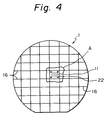
- Figure 2A shows many similar IC chips ll formed on a wafer, wherein the IC chips ll have been separated from each other by cutting the slice line l6 of the wafer, and as also shown in Fig. 2A, an IC element forming the region l2 is connected to pad electrodes l5 through aluminum wiring l4.
- the electrodes l5 are formed by wire bonding to the pad electrodes l5.
- Figure 2B shows a cross-sectional view of Fig. 2A.
- l9 and 20 denote lead-frame and ceramic, respectively.
- Figure 3 shows a side view of an example according to the present invention.
- Figure 3 shows a wafer set 4 of two silicon wafers l and a heat sink plate 3 interposed therebetween.
- the heat sink plate is made of, for example, aluminum and copper.
- the sets 4 are stacked in a wafer stacked body 6, and the ends of the heat sink plate 3 are exposed at side surfaces 8 thereof.
- Intermediate connecting circuits 9 connecting and controlling the semiconductor elements 2 are provided on a surface of a multi-layer semiconductor IC device 7.
- Transistors, capacitors, resistances, etc., are formed on a polished side surface 8 of a semiconductor wafer together with wirings.
- the semiconductor wafers 1 are connected through an insulating layer 5.
- semiconductor elements are formed on a (l00) surface of a silicon wafer l, and IC chips ll (only one chip shown) are formed in a suitable position so that side surface circuits can be formed together in a subsequent process.
- the lines l6 denote the slice lines.
- Alignment marks 22 are provided on the IC chip ll.
- Figure 5 is an enlarged view of a portion A of Fig. 4.
- the electrical connections between the stacked IC chips in the present invention are carried out on a side surface of an IC chip.
- the output electrodes drawn from the integrated elements are embedded in a slice surface.
- Aluminum lead wiring is formed at the same time as the aluminum wiring is finally formed during the formation of the integrated semiconductor element region l2.
- the aluminum lead wiring is connected to the embedded electrodes 24 formed along the slice lines l6.
- This aluminum wiring 25 is formed by a process wherein a l ⁇ m thick aluminum layer is formed by a sputtering process and patterned.
- the embedded electrodes 24 are 20 ⁇ m in width and l00 ⁇ m in length from slice line. After the formation of the electrode, a usual passivation film is formed.
- Fig. 6 is a schematic cross-sectional view taken along a slice line of Fig. 5. As shown in Fig. 6, on the output electrodes 24 a passivation layer 26 is provided. A method for producing a base unit structure consisting of an aluminum plate and silicon wafers connected through the aluminum plate will now be described.
- an IC side surface of a silicon wafer l is adhered to a supporting quartz plate 30a by a thermoplastic resin 3l such as picene.
- a back, non-adhered surface of the silicon wafer l is polished for reducing thickness to a total thickness of 200 ⁇ m.
- the supporting quartz plate 30a is aligned with the silicon wafer by an alignment mark 22.
- Another similar structure is formed and, as shown in Fig. 8, the two structures are permanently bonded to an aluminum plate 3 having a thickness of, for example, 0.05 to l mm, by silver paste or Au-Sn solder 33.
- thermoplastic resin is heated and melted and the quartz plates 30a on both sides are separated from the silicon wafers l so that a base unit structure consisting of a heat sink aluminum plate 3 and silicon wafers 1 is formed.
- the base unit structure is cleaned by trichlene.
- one base unit structure is connected to another base unit structure by a silicone resin 35.
- One of the base unit structures is fixed to a quartz plate 30b by vacuum chucking, and other base unit structure is permanently bonded to a ceramic substrate 40 by a silicone resin such as PLOS (polyladder organosiloxane).
- PLOS polyladder organosiloxane
- the IC chip can be cooled enough by an aluminum plate having a thickness of 70 ⁇ m.
- the thickness of cooling metal plate will be calculated.
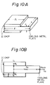
- Fig. 10A is an example for explaining thermal resistance and Fig. 10B is an equivalence thermal circuit diagram of Fig 10A.
- R c , R e and R sink are a contact thermal resistance between an IC chip and a metal plate, an average thermal resistance of a metal plate, and contact thermal resistance with a heat sink.
- the thicknesses(d) of aluminum and copper cooling plates are 0.07 and 0.042 cm respectively.
- an aluminum plate having a thickness of 0.5 mm is used. Consequently, the total thickness of the two IC chips and the aluminum plate is about 1 mm. Since a 20 x 20 mm chip is formed on the 152.4 mm (6 inches) silicon wafer, it is better that twenty base unit structures are stacked to form a three-dimensional IC cubic unit. Furthermore, to increase the efficiency of the formation of the side surface wiring structure, it is best that one hundred basic units of five layers of three-dimentional IC cubic units or more are stacked, whereby the production efficiency of the side surface wiring is increased five-fold. The width of the side surface of only 20 basic units is 20 mm. On the other hand, since the size of a mask to form side surface circuits is 150 mm or more,five layers of the IC cubic unit must be formed so as not to make wasted space.
- the stacked structure is shown in Fig. ll.
- a slice B shown in Fig. l2 and Fig. ll is obtained.
- both the sliced surfaces should be polished to a mirror surface in which an embedded electrode has been previously exposed, to get smoothness.
- IC cubic units of the same number of IC chips formed on a wafer can be produced.
- Fig. ll 5 sets of 20 layers of the basic unit structure are stacked.
- An advantage of an embodiment of the present invention resides in that after stacking of a lot of the IC cubic units,slices are produced and side surface circuits can be collectively formed using one mask by a well known process. As shown in Fig. 12 the heat sink side is the back side of the wiring side.
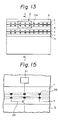
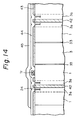
- Figure l3 shows an enlarged view of a polished wiring side portion of Fig. l2, and Fig. l4 shows a cross-sectional view thereof taken along a line C-C of Fig. l3.
- Fig. l the aluminum plates 3, silicon wafers l, device formation layer 3a, adhesive layers 33 and embedded electrodes 24 are exposed.
- a 500 nm thick SiO2 layer 43 is first formed on the entire silicon wafer by a well known chemical vapour deposition (CVD) process. Then, after for example the SiO2 of a transistor formation region is removed, a gate oxide film is formed by laser oxidation, a tungstensilicide gate metal is formed, and a source and a drain are formed by ion-implanting and laser annealing processes, so that a MOS transistor is formed.
- CVD chemical vapour deposition
- Fig. l5 41 and 25 denote an aluminum bonding pad and an aluminum wiring, respectively.
- the silicone resin adhesive layer is etched by oxygen plasma and a silicon substrate is etched selectively by a mixed etchant including HClO4 and H3PO4 , so that an aluminum plate having an end extended for l ⁇ m can be obtained.
- a mixed etchant including HClO4 and H3PO4
- the etching is simultaneously carried out in all IC cubic units included in the slice of Fig. 11.
- a slice shown in Fig. l2 is further cut to a three-dimensional IC cubic unit (20 x 20 x 20 mm), a surface other than a heat sink surface is covered by a polyimide, and a pad aluminum electrode is opened so that a structure shown in Fig. l6 is obtained.
- Fig. l6, 52 is an aluminum heat sink having dissipating fins.
- Grooves to be fixed to the extended aluminum plate by solder 49 are provided on a surface of the aluminum heat sink 52.
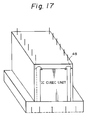
- Figure l7 shows a structure of a three-dimensional IC package according to an example of the present invention.
- Figure l8 shows another example of the present invention.
- a multi-layer semiconductor IC device 7 has flat side surfaces 8, one of which is adhered to a large heat sink plate 50 with solder.
- an intermediate connecting circuit 9 is provided on a surface of the structure. Accordingly, as aluminum plates for dissipation are connected to the large heat sink plate, the heat sink effects during operation are improved.
Landscapes
- Engineering & Computer Science (AREA)
- Power Engineering (AREA)
- Microelectronics & Electronic Packaging (AREA)
- Computer Hardware Design (AREA)
- Physics & Mathematics (AREA)
- Condensed Matter Physics & Semiconductors (AREA)
- General Physics & Mathematics (AREA)
- Chemical & Material Sciences (AREA)
- Materials Engineering (AREA)
- Cooling Or The Like Of Semiconductors Or Solid State Devices (AREA)
- Container, Conveyance, Adherence, Positioning, Of Wafer (AREA)
Applications Claiming Priority (2)
| Application Number | Priority Date | Filing Date | Title |
|---|---|---|---|
| JP60131009A JPS61288455A (ja) | 1985-06-17 | 1985-06-17 | 多層半導体装置の製造方法 |
| JP131009/85 | 1985-06-17 |
Publications (3)
| Publication Number | Publication Date |
|---|---|
| EP0206696A2 EP0206696A2 (en) | 1986-12-30 |
| EP0206696A3 EP0206696A3 (en) | 1988-08-10 |
| EP0206696B1 true EP0206696B1 (en) | 1992-06-10 |
Family
ID=15047836
Family Applications (1)
| Application Number | Title | Priority Date | Filing Date |
|---|---|---|---|
| EP86304575A Expired - Lifetime EP0206696B1 (en) | 1985-06-17 | 1986-06-13 | Multi-layer semiconductor device |
Country Status (5)
| Country | Link |
|---|---|
| US (1) | US5051865A (enExample) |
| EP (1) | EP0206696B1 (enExample) |
| JP (1) | JPS61288455A (enExample) |
| KR (1) | KR900008973B1 (enExample) |
| DE (1) | DE3685612T2 (enExample) |
Families Citing this family (63)
| Publication number | Priority date | Publication date | Assignee | Title |
|---|---|---|---|---|
| US4954875A (en) * | 1986-07-17 | 1990-09-04 | Laser Dynamics, Inc. | Semiconductor wafer array with electrically conductive compliant material |
| FR2634064A1 (fr) * | 1988-07-05 | 1990-01-12 | Thomson Csf | Composant electronique a couche de conductivite thermique elevee |
| US5038201A (en) * | 1988-11-08 | 1991-08-06 | Westinghouse Electric Corp. | Wafer scale integrated circuit apparatus |
| CA2049979A1 (en) * | 1990-01-24 | 1991-07-25 | Jury D. Sasov | Three-dimensional electronic unit and method of fabricating same |
| JP3058898B2 (ja) * | 1990-09-03 | 2000-07-04 | 三菱電機株式会社 | 半導体装置及びその評価方法 |
| JPH0817221B2 (ja) * | 1990-11-13 | 1996-02-21 | 株式会社東芝 | 半導体装置及び半導体ウェーハの実装方法 |
| US5847448A (en) * | 1990-12-11 | 1998-12-08 | Thomson-Csf | Method and device for interconnecting integrated circuits in three dimensions |
| US5451550A (en) * | 1991-02-20 | 1995-09-19 | Texas Instruments Incorporated | Method of laser CVD seal a die edge |
| JPH0513666A (ja) * | 1991-06-29 | 1993-01-22 | Sony Corp | 複合半導体装置 |
| US5202754A (en) * | 1991-09-13 | 1993-04-13 | International Business Machines Corporation | Three-dimensional multichip packages and methods of fabrication |
| JPH0715969B2 (ja) * | 1991-09-30 | 1995-02-22 | インターナショナル・ビジネス・マシーンズ・コーポレイション | マルチチツプ集積回路パツケージ及びそのシステム |
| US5691885A (en) * | 1992-03-17 | 1997-11-25 | Massachusetts Institute Of Technology | Three-dimensional interconnect having modules with vertical top and bottom connectors |
| ATE145292T1 (de) * | 1992-03-17 | 1996-11-15 | Massachusetts Inst Technology | Geringbenachbarte dreidimensionale verbindung. |
| DE4211899C2 (de) * | 1992-04-09 | 1998-07-16 | Daimler Benz Aerospace Ag | Mikrosystem-Laseranordnung und Mikrosystem-Laser |
| JPH0779144B2 (ja) * | 1992-04-21 | 1995-08-23 | インターナショナル・ビジネス・マシーンズ・コーポレイション | 耐熱性半導体チップ・パッケージ |
| US5343366A (en) * | 1992-06-24 | 1994-08-30 | International Business Machines Corporation | Packages for stacked integrated circuit chip cubes |
| US5854534A (en) * | 1992-08-05 | 1998-12-29 | Fujitsu Limited | Controlled impedence interposer substrate |
| DE69330450T2 (de) * | 1992-08-05 | 2001-11-08 | Fujitsu Ltd., Kawasaki | Dreidimensionaler Multichipmodul |
| US5313097A (en) * | 1992-11-16 | 1994-05-17 | International Business Machines, Corp. | High density memory module |
| US5561622A (en) * | 1993-09-13 | 1996-10-01 | International Business Machines Corporation | Integrated memory cube structure |
| US5502667A (en) * | 1993-09-13 | 1996-03-26 | International Business Machines Corporation | Integrated multichip memory module structure |
| US5596226A (en) * | 1994-09-06 | 1997-01-21 | International Business Machines Corporation | Semiconductor chip having a chip metal layer and a transfer metal and corresponding electronic module |
| US5521434A (en) * | 1994-10-17 | 1996-05-28 | International Business Machines Corporation | Semiconductor chip and electronic module with integrated surface interconnects/components |
| US5818112A (en) * | 1994-11-15 | 1998-10-06 | Siemens Aktiengesellschaft | Arrangement for capacitive signal transmission between the chip layers of a vertically integrated circuit |
| US5701037A (en) * | 1994-11-15 | 1997-12-23 | Siemens Aktiengesellschaft | Arrangement for inductive signal transmission between the chip layers of a vertically integrated circuit |
| US5609772A (en) * | 1995-06-05 | 1997-03-11 | International Business Machines Corporation | Cube maskless lead open process using chemical mechanical polish/lead-tip expose process |
| US5719745A (en) * | 1995-07-12 | 1998-02-17 | International Business Machines Corporation | Extended surface cooling for chip stack applications |
| US5648684A (en) * | 1995-07-26 | 1997-07-15 | International Business Machines Corporation | Endcap chip with conductive, monolithic L-connect for multichip stack |
| DE19543540C1 (de) * | 1995-11-22 | 1996-11-21 | Siemens Ag | Vertikal integriertes Halbleiterbauelement mit zwei miteinander verbundenen Substraten und Herstellungsverfahren dafür |
| US5763943A (en) * | 1996-01-29 | 1998-06-09 | International Business Machines Corporation | Electronic modules with integral sensor arrays |
| US5952725A (en) | 1996-02-20 | 1999-09-14 | Micron Technology, Inc. | Stacked semiconductor devices |
| US5673218A (en) | 1996-03-05 | 1997-09-30 | Shepard; Daniel R. | Dual-addressed rectifier storage device |
| US6784023B2 (en) * | 1996-05-20 | 2004-08-31 | Micron Technology, Inc. | Method of fabrication of stacked semiconductor devices |
| US5815374A (en) * | 1996-09-30 | 1998-09-29 | International Business Machines Corporation | Method and apparatus for redirecting certain input/output connections of integrated circuit chip configurations |
| US5781413A (en) * | 1996-09-30 | 1998-07-14 | International Business Machines Corporation | Method and apparatus for directing the input/output connection of integrated circuit chip cube configurations |
| US5835396A (en) * | 1996-10-17 | 1998-11-10 | Zhang; Guobiao | Three-dimensional read-only memory |
| SE511425C2 (sv) * | 1996-12-19 | 1999-09-27 | Ericsson Telefon Ab L M | Packningsanordning för integrerade kretsar |
| US6075287A (en) * | 1997-04-03 | 2000-06-13 | International Business Machines Corporation | Integrated, multi-chip, thermally conductive packaging device and methodology |
| US6551857B2 (en) | 1997-04-04 | 2003-04-22 | Elm Technology Corporation | Three dimensional structure integrated circuits |
| US5793103A (en) * | 1997-05-08 | 1998-08-11 | International Business Machines Corporation | Insulated cube with exposed wire lead |
| JP3501644B2 (ja) | 1998-02-02 | 2004-03-02 | 日本電気株式会社 | 半導体パッケージの熱抵抗計算方法および記録媒体および熱抵抗計算装置 |
| WO2000007240A1 (en) * | 1998-07-27 | 2000-02-10 | Reveo, Inc. | Three-dimensional packaging technology for multi-layered integrated circuits |
| JP2001352035A (ja) * | 2000-06-07 | 2001-12-21 | Sony Corp | 多層半導体装置の組立治具及び多層半導体装置の製造方法 |
| US6956757B2 (en) | 2000-06-22 | 2005-10-18 | Contour Semiconductor, Inc. | Low cost high density rectifier matrix memory |
| US6727422B2 (en) | 2000-09-18 | 2004-04-27 | Chris Macris | Heat sink/heat spreader structures and methods of manufacture |
| US6743972B2 (en) | 2000-09-18 | 2004-06-01 | Chris Macris | Heat dissipating IC devices |
| US6818817B2 (en) | 2000-09-18 | 2004-11-16 | Chris Macris | Heat dissipating silicon-on-insulator structures |
| US20030002267A1 (en) * | 2001-06-15 | 2003-01-02 | Mantz Frank E. | I/O interface structure |
| US6945054B1 (en) * | 2002-10-04 | 2005-09-20 | Richard S. Norman | Method and apparatus for cooling microelectronic complexes including multiple discrete functional modules |
| US6856010B2 (en) * | 2002-12-05 | 2005-02-15 | Staktek Group L.P. | Thin scale outline package |
| JP4554152B2 (ja) * | 2002-12-19 | 2010-09-29 | 株式会社半導体エネルギー研究所 | 半導体チップの作製方法 |
| JP2004311464A (ja) | 2003-04-01 | 2004-11-04 | Renesas Technology Corp | 半導体装置 |
| US20040207990A1 (en) * | 2003-04-21 | 2004-10-21 | Rose Andrew C. | Stair-step signal routing |
| JP4238998B2 (ja) | 2004-03-18 | 2009-03-18 | セイコーエプソン株式会社 | 電気デバイス |
| US7999383B2 (en) | 2006-07-21 | 2011-08-16 | Bae Systems Information And Electronic Systems Integration Inc. | High speed, high density, low power die interconnect system |
| WO2008139605A1 (ja) * | 2007-05-14 | 2008-11-20 | Kabushiki Kaisha Nihon Micronics | 積層型パッケージ、及び、積層型パッケージの形成方法 |
| US7813157B2 (en) * | 2007-10-29 | 2010-10-12 | Contour Semiconductor, Inc. | Non-linear conductor memory |
| WO2009061834A1 (en) * | 2007-11-05 | 2009-05-14 | Contour Semiconductor, Inc. | Low-cost, high-density rectifier matrix memory |
| US20090225621A1 (en) * | 2008-03-05 | 2009-09-10 | Shepard Daniel R | Split decoder storage array and methods of forming the same |
| US20090296445A1 (en) * | 2008-06-02 | 2009-12-03 | Shepard Daniel R | Diode decoder array with non-sequential layout and methods of forming the same |
| US8325556B2 (en) * | 2008-10-07 | 2012-12-04 | Contour Semiconductor, Inc. | Sequencing decoder circuit |
| US8772920B2 (en) * | 2011-07-13 | 2014-07-08 | Oracle International Corporation | Interconnection and assembly of three-dimensional chip packages |
| MY192051A (en) * | 2016-12-29 | 2022-07-25 | Intel Corp | Stacked dice systems |
Family Cites Families (16)
| Publication number | Priority date | Publication date | Assignee | Title |
|---|---|---|---|---|
| US3243660A (en) * | 1966-03-29 | Electroni c module as sbmbly | ||
| GB1083200A (en) * | 1966-08-17 | 1967-09-13 | Standard Telephones Cables Ltd | Improvements in or relating to semiconductor devices |
| DE1591105A1 (de) * | 1967-12-06 | 1970-09-24 | Itt Ind Gmbh Deutsche | Verfahren zum Herstellen von Festkoerperschaltungen |
| US3705332A (en) * | 1970-06-25 | 1972-12-05 | Howard L Parks | Electrical circuit packaging structure and method of fabrication thereof |
| US3704455A (en) * | 1971-02-01 | 1972-11-28 | Alfred D Scarbrough | 3d-coaxial memory construction and method of making |
| US4283754A (en) * | 1979-03-26 | 1981-08-11 | Bunker Ramo Corporation | Cooling system for multiwafer high density circuit |
| US4546406A (en) * | 1980-09-25 | 1985-10-08 | Texas Instruments Incorporated | Electronic circuit interconnection system |
| JPS5839055A (ja) * | 1981-08-31 | 1983-03-07 | Matsushita Electric Ind Co Ltd | 半導体装置 |
| US4500905A (en) * | 1981-09-30 | 1985-02-19 | Tokyo Shibaura Denki Kabushiki Kaisha | Stacked semiconductor device with sloping sides |
| JPS5890744A (ja) * | 1981-11-25 | 1983-05-30 | Mitsubishi Electric Corp | 半導体装置 |
| JPS5891664A (ja) * | 1981-11-26 | 1983-05-31 | Mitsubishi Electric Corp | 積層構造半導体装置 |
| US4514784A (en) * | 1983-04-22 | 1985-04-30 | Cray Research, Inc. | Interconnected multiple circuit module |
| US4628407A (en) * | 1983-04-22 | 1986-12-09 | Cray Research, Inc. | Circuit module with enhanced heat transfer and distribution |
| WO1985002283A1 (en) * | 1983-11-07 | 1985-05-23 | Irvine Sensors Corporation | Detector array module-structure and fabrication |
| JPS6118164A (ja) * | 1984-07-04 | 1986-01-27 | Mitsubishi Electric Corp | 半導体装置 |
| US4698662A (en) * | 1985-02-05 | 1987-10-06 | Gould Inc. | Multichip thin film module |
-
1985
- 1985-06-17 JP JP60131009A patent/JPS61288455A/ja active Granted
-
1986
- 1986-06-13 KR KR1019860004722A patent/KR900008973B1/ko not_active Expired
- 1986-06-13 EP EP86304575A patent/EP0206696B1/en not_active Expired - Lifetime
- 1986-06-13 DE DE8686304575T patent/DE3685612T2/de not_active Expired - Fee Related
-
1991
- 1991-03-11 US US07/667,257 patent/US5051865A/en not_active Expired - Fee Related
Also Published As
| Publication number | Publication date |
|---|---|
| JPH0528503B2 (enExample) | 1993-04-26 |
| EP0206696A2 (en) | 1986-12-30 |
| DE3685612D1 (de) | 1992-07-16 |
| JPS61288455A (ja) | 1986-12-18 |
| US5051865A (en) | 1991-09-24 |
| KR870000760A (ko) | 1987-02-20 |
| KR900008973B1 (ko) | 1990-12-15 |
| DE3685612T2 (de) | 1993-01-28 |
| EP0206696A3 (en) | 1988-08-10 |
Similar Documents
| Publication | Publication Date | Title |
|---|---|---|
| EP0206696B1 (en) | Multi-layer semiconductor device | |
| KR102585450B1 (ko) | 브레이징된 전기 전도성 층을 포함하는 칩 캐리어를 구비한 몰딩된 패키지 | |
| US7557434B2 (en) | Power electronic package having two substrates with multiple electronic components | |
| US8432030B2 (en) | Power electronic package having two substrates with multiple semiconductor chips and electronic components | |
| US5547906A (en) | Methods for producing integrated circuit devices | |
| US6117707A (en) | Methods of producing integrated circuit devices | |
| CN101202266B (zh) | 芯片级封装及其制造方法和大功率集成电路器件 | |
| US6040235A (en) | Methods and apparatus for producing integrated circuit devices | |
| US5475264A (en) | Arrangement having multilevel wiring structure used for electronic component module | |
| JPS6355213B2 (enExample) | ||
| JPH0831560B2 (ja) | 回路パツケージ・アセンブリ | |
| CN111244041A (zh) | 包括两种不同导电材料的芯片接触元件的封装 | |
| JP4094075B2 (ja) | ワイヤボンドなしモジュールパッケージおよび製造方法 | |
| JP2022181818A (ja) | 半導体装置 | |
| KR840006747A (ko) | 배선 기판과 그 제조방법 및 이를 사용한 반도체 장치 | |
| JP2022181822A (ja) | 半導体装置 | |
| JP2022181813A (ja) | 半導体装置 | |
| JPH08306861A (ja) | チップ抵抗体 | |
| WO2022249814A1 (ja) | 半導体装置 | |
| CN117790462B (zh) | 一种提高陶瓷基板利用率的叠层陶瓷基板结构及功率模块 | |
| JP2022181817A (ja) | 半導体装置 | |
| CN114975130B (zh) | 一种垂直型mosfet芯片的封装结构的封装方法 | |
| GB2485087A (en) | Power electronic package | |
| US6846697B2 (en) | Integrated circuit packages and the method for making the same | |
| JP2023122391A (ja) | 半導体装置 |
Legal Events
| Date | Code | Title | Description |
|---|---|---|---|
| PUAI | Public reference made under article 153(3) epc to a published international application that has entered the european phase |
Free format text: ORIGINAL CODE: 0009012 |
|
| AK | Designated contracting states |
Kind code of ref document: A2 Designated state(s): DE FR GB |
|
| PUAL | Search report despatched |
Free format text: ORIGINAL CODE: 0009013 |
|
| AK | Designated contracting states |
Kind code of ref document: A3 Designated state(s): DE FR GB |
|
| 17P | Request for examination filed |
Effective date: 19881007 |
|
| 17Q | First examination report despatched |
Effective date: 19910201 |
|
| GRAA | (expected) grant |
Free format text: ORIGINAL CODE: 0009210 |
|
| AK | Designated contracting states |
Kind code of ref document: B1 Designated state(s): DE FR GB |
|
| REF | Corresponds to: |
Ref document number: 3685612 Country of ref document: DE Date of ref document: 19920716 |
|
| ET | Fr: translation filed | ||
| PLBE | No opposition filed within time limit |
Free format text: ORIGINAL CODE: 0009261 |
|
| STAA | Information on the status of an ep patent application or granted ep patent |
Free format text: STATUS: NO OPPOSITION FILED WITHIN TIME LIMIT |
|
| 26N | No opposition filed | ||
| PGFP | Annual fee paid to national office [announced via postgrant information from national office to epo] |
Ref country code: FR Payment date: 19930629 Year of fee payment: 8 |
|
| PG25 | Lapsed in a contracting state [announced via postgrant information from national office to epo] |
Ref country code: FR Effective date: 19950228 |
|
| REG | Reference to a national code |
Ref country code: FR Ref legal event code: ST |
|
| PGFP | Annual fee paid to national office [announced via postgrant information from national office to epo] |
Ref country code: GB Payment date: 19960604 Year of fee payment: 11 |
|
| PGFP | Annual fee paid to national office [announced via postgrant information from national office to epo] |
Ref country code: DE Payment date: 19960612 Year of fee payment: 11 |
|
| PG25 | Lapsed in a contracting state [announced via postgrant information from national office to epo] |
Ref country code: GB Free format text: LAPSE BECAUSE OF NON-PAYMENT OF DUE FEES Effective date: 19970613 |
|
| GBPC | Gb: european patent ceased through non-payment of renewal fee |
Effective date: 19970613 |
|
| PG25 | Lapsed in a contracting state [announced via postgrant information from national office to epo] |
Ref country code: DE Free format text: LAPSE BECAUSE OF NON-PAYMENT OF DUE FEES Effective date: 19980303 |