EP0196647B1 - Digitales Übertragungssystem - Google Patents
Digitales Übertragungssystem Download PDFInfo
- Publication number
- EP0196647B1 EP0196647B1 EP86104383A EP86104383A EP0196647B1 EP 0196647 B1 EP0196647 B1 EP 0196647B1 EP 86104383 A EP86104383 A EP 86104383A EP 86104383 A EP86104383 A EP 86104383A EP 0196647 B1 EP0196647 B1 EP 0196647B1
- Authority
- EP
- European Patent Office
- Prior art keywords
- bits
- bit stream
- data bit
- error
- word
- Prior art date
- Legal status (The legal status is an assumption and is not a legal conclusion. Google has not performed a legal analysis and makes no representation as to the accuracy of the status listed.)
- Expired - Lifetime
Links
Images


Classifications
-
- H—ELECTRICITY
- H04—ELECTRIC COMMUNICATION TECHNIQUE
- H04L—TRANSMISSION OF DIGITAL INFORMATION, e.g. TELEGRAPHIC COMMUNICATION
- H04L7/00—Arrangements for synchronising receiver with transmitter
- H04L7/04—Speed or phase control by synchronisation signals
- H04L7/048—Speed or phase control by synchronisation signals using the properties of error detecting or error correcting codes, e.g. parity as synchronisation signal
Definitions
- the present invention relates to a synchronization circuit for a digital radio communication system having an error correction circuit.
- an input signal is processed by a transmit code processor 40 at the transmitting end of the system to produce a data bit stream which is fed to an error correction encoder 42 where error correcting codes are added and modulated by a transmitter 43 and sent over a radio link to a receiving end of the link.
- the signal is demodulated by a receiver 46 and fed to an error correction decoder 45 to correct data bits in error and applied to a receive code processor 44 to treat it in a process inverse to that of transmit code processor 40.
- Figs. 10 and 11 Details of the transmit code processor 40, error correction encoder 42, error correction decoder 45 and receiver code processor 44 are shown in Figs. 10 and 11 (see also "An Introduction to Digital Integrated Communications Systems", Hiroshi Inose, University of Tokyo Press (1979)).
- transmit code processor 40 includes a multiplexer 51 to which a main signal and an auxiliary signal are applied.
- a timing signal generator 52 generates a timing output pulse which causes a frame sync generator 53 to supply a frame sync code to the multiplexer 51.
- Input data signals are multiplexed with the frame sync code into an output data stream in response to a timing signal from generator 52 and fed to a data compression memory 54 of the error correction encoder 42.
- Error correction encoder 42 is provided with a timing signal generator 56 whose output determines the rate of compression of the time dimension of data.
- Compression memory 54 compresses into groups of clusttered data bits to allow time slots into which redundant bits are to be inserted.
- the time-compressed data bits are fed to a redundant bit generator 55 to allow it detect timing for bit insertion and generate error correction redundant bits which are inserted to the time-compressed data stream by a bit adder 57 and sent to the receiver 46 at the receiving end.
- error correction decoder 45 includes a delay circuit 61 and a redundant bit decoder 62 to both of which the output of receiver 46 is applied.
- Decoder 62 supplies a syndrome to an error corrector 64 and a word synchronizer 65.
- Word synchronizer 65 supplies a hunting pulse to a timing signal generator 63 to cause it to be word synchronized.
- the input signal applied to delay circuit 61 is delayed until redundant bit decoding operation is complete and fed to error corrector 64.
- Data bits in error are corrected using the syndrome supplied from decoder 62 and fed to a data expansion memory circuit 66 where the time dimension of the data is recovered, while removing the inserted redundant bits.
- expansion memory circuit 66 The output of expansion memory circuit 66 is applied to a frame synchronizer 68 which detects the frame sync code by checking it against a frame sync code generated by a frame sync generator 70 and supplies a hunting pulse to a timing signal generator 69 to cause it to generate a timing signal to frame sync generator 70 at frame-synchronized timing.
- Input data from memory circuit 66 is demultiplexed into separate signals by a timing signal received from generator 69.
- EP-A-0 100 818 describes a synchronous communication system with no parity error detection during periods in which word synchronization cannot be established with the result of a false frame synchronization.
- US-A-3,806,647 describes a phase ambiguity resolution system with the use of syndromes for QPSK demodulation to eliminate carrier phase ambiguities.
- This object is solved with the features of the claims.
- the invention eliminates the need for inserting frame synchronization codes which would otherwise occupy time slots for data bits and provides transmission efficiency by modulo-summing sync bits with error correcting redundant bits derived from a data bit stream.
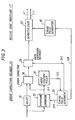
- Fig. 1 is a block diagram of a digital radio communication system embodying the present invention.
- the system of the invention comprises, at the transmitting end of a radio transmission link, transmit code processor 10, error correcting encoder 11 and transmitter 12, and at the receiving end, it comprises receiver 13, error correction decoder 14 and receive code processor 15.
- the system of the invention differs from the prior art in that transmit code processor 10 sends a bit-sync timing signal on a bus 106 to error correction encoder 11 which sends back a frame-sync timing signal on bus 105, and in that error correction decoder 14 sends a timing pulse on a bus 111 to receive code processor 15. Details of the transmit code processor 10, error correction encoder 11 error correction decoder 14 and receive code processor 15 are shown in Figs. 2 and 3.
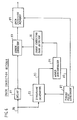
- an input main digital signal which is received on a high frequency, main channel and an input auxiliary digital signal which is received on a low frequency, service channel, are applied to a multiplexer 21 where they are multiplexed together in response to a timing pulse supplied on bus 204 from a timing pulse generator 22 so that each data bit of the auxiliary signal is multiplexed in synchronizm with a frame synchronization timing signal which is supplied on bus 105 from a timing pulse generator 24 of the error correction encoder 11.
- timing pulse generator 22 initially establishes bit-synchronous operation in response to a proper timing pulse supplied on bus 205 from the multiplexer 21 and applies a bit-synchronization timing pulse on bus 106 to a timing pulse generator 24 which sends a frame-synchronization timing pulse on bus 105 back to the timing pulse generator 22.
- the multiplexed data bit stream is supplied from multiplexer 21 on bus 203 to a data compression memory circuit 23 of error correction encoder 11 to compress the time dimension of the multiplexed signal to allow redundant bits to be inserted thereto.
- the timing pulse generator 24 generates a signal representing the position of time slots into which redundant bits are to be inserted and supplies it on buses 208 and 209 to compression memory circuit 23 and to a redundant bit generator 25 respectively, and further generates sync bits "010" concurrently with the generation of the frame synchronization timing signal on bus 105 and supplies it on bus 208 to the memory circuit 23. Therefore, the sync bits "010" are time-coincident with the time slots of the redundant bits which immediately precede each data bit of the auxiliary-channel signal.
- Redundant bit generator 25 derives error correcting redundant bits from the output of memory circuit 23 in response to the position indicating signal on bus 209, supplies the redundant bits on bus 210 to a bit adder 26 where they are modulo-summed with the sync bits to produce a composite data bit stream (Fig. 4) which is applied through output bus 213 to transmitter 12 and transmitted to the receiving station.
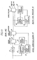
- the transmitted signal is received by receiver 13 and fed to a delay circuit 31 of error correction decoder 14 and to a redundant bit decoder, or syndrome generator 32.
- Syndrome generator 32 derives a syndrome from the input data and supplies it on bus 303 to a word synchronizer 35.
- Word synchronizer 35 monitors the syndromes detects the modulo-summed sync bits from the monitored syndromes and causes syndrome generator 32 to word-synchronize with input data words.
- word synchronizer 35 asynchronously generates a hunting pulse in response to the detection of the sync bits and supplies it on bus 306 to timing pulse generator 33 to cause it to generate a signal indicating the position of time slots in which the redundant bits have been inserted and supplies the position indicating signal on line 304 to syndrome generator 32 and on line 307 to a data expansion memory circuit 36.
- syndrome generator 32 uses the position indicating signal, syndrome generator 32 performs the decoding of the redundant bits to generate syndromes.
- the input data stream is delayed by delay circuit 31 so that its output is time-coincident with the syndrome supplied from syndrome generator 32 to perform detection and correction of data bits in errors.
- the error-corrected data is applied to data expansion memory circuit 36 which removes the redundant bits from the data bit stream using the position indicating signal supplied on line 307 and expands the time dimension of the bit stream.
- the output of the data expansion memory circuit 36 is applied to the receive code processor 15.
- word synchronizer 35 Since the input data contains an error correction sync word "010" at frame intervals, word synchronizer 35 identifies a syndrome containing a word "010” and signals the timing pulse generator 33 on bus 306 to generate a timing pulse immediately preceding each of the auxiliary channel data bits. This timing pulse is applied on line 308 to a timing pulse generator 38 of receive code processor 15 which passes it at proper timing to a demultiplexer 37. Demultiplexer 37 separates the input data bit stream into the original main and auxiliary channel data streams on buses 311 and 312 in response to the output of timing pulse generator 38.
- Fig. 5 is a block diagram of an error correction encoder at the transmitting end of the system according to a second embodiment of the present invention in which word synchronization is utilized to eliminate the need for inserting frame sync codes.
- an input digital signal applied on input bus 70 to a data compression memory circuit 71 comprises three parallel data bit streams each including a series of 81-bit data words of the main channel as shown at Fig. 7A. For purposes of illustration, description on the auxiliary channel signal is omitted.
- the time dimension of the data bit streams is compressed to allow additional three binary "0" bits to be inserted to each data bit stream as sync bits in response to a timing pulse supplied from timing pulse generator 72 to form a series of 84-bit words on each data bit stream on output bus 73 (see Fig. 7A).
- the output signal from data compression memory circuit 71 is fed to a redundant bit adder 74 and to a redundant bit generator 75. Redundant bit generator 75 arithmetically divides (81 x 3) data bits and supplies (3 x 3) bits of residue on output bus 76 to bit adder 74 (see Fig. 7A).
- Redundant bit adder 74 provides modulo-summation of the (3 x 3)-bit residue with the all-zero three bits of the 84-bit data bit streams from compression memory 71, producing three 84-bit data streams on output bus 77 for application to the transmitter 12 (see Fig. 7B).
- Fig. 6 is a block diagram of the error correction decoder circuit at the receiving end of the transmission system associated with the error correction encoder of Fig. 5.
- three data bits streams on input bus 80 are applied to delay circuit 81 and to a redundant bit decoder, or syndrome generator 82.
- Syndrome generator 82 divides the three input data bit streams of 81 bits each and derives three data bit streams of 3 bits each as a residue of the division on output bus 83.
- the same residue as the residue generated by redundant bit generator 75, Fig. 5 is obtained on the output bus 83 of syndrome generator 82 (see Fig. 7B) and all-zero bits are delivered from syndrome generator 82. If error occurs during transmission, the output syndrome on bus 83 differs from the residue at the transmitting end (see Fig. 7B).
- the output of syndrome generator 82 is applied to a word synchronizer 84.
- the word synchronizer 84 comprises a timing converter, or serial-to-parallel converter 90 which converts the timing of input syndrome from syndrome generator 82 so that the three bits of each syndrome bit sequence are time-coincident with each other and nine (9) parallel syndrome bits are applied simultaneously to an AND gate 91 and to an error correcting code detector 85. In the absence of error bits, all zero bits are fed to correcting code detector 85.
- the output of AND gate 91 is applied to a counter 92 having a hysteresis to detect an error bit in the received data bit streams by counting the occurrences of logical "1" at the output of AND gate 91. Once a full count is reached in the hysteresis counter, the full count is maintained for a prescribed period to prevent undesirable fluctuations. Likewise, when a zero count is reached, it is maintained for a prescribed period.
- the output of counter 92 is applied as a hunting pulse on line 86 to a timing pulse generator 87, Fig. 6. This hunting pulse is repeatedly generated until all zero bits are presented to the inputs of AND gate 91, whereupon word synchronization is established.
- An error bit is detected from the nine-parallel input bits by detector 85 which derives therefrom an error correcting code indicating the time slot of the data bit stream in which the error has occurred and applies it to an error corrector 88.
- the input data bit stream, which has been delayed by the delay circuit 81, is applied to error corrector 88 and error bits which might exist therein are corrected by the output of error correcting code detector 85.
- the error-corrected data bit streams are applied to a data expansion memory 89 where the (3 x 3) redundant bits are removed and data bits are expanded in time dimension in response to a timing pulse supplied from timing pulse generator 87.
- Timing pulse generator 87 responds to the hunting pulse from word synchronizer 84 to word-synchronously supplies a timing signal to syndrome generator 82.
Claims (3)
- Digitales Übertragungssystem, das aufweist:a) einen Sender mit einer Fehlerkorrekturcodierereinrichtung (25) zur Ableitung von Redundanzbits aus einem Datenbitstrom undb) einen Empfänger mitb₁) einer Fehlerkorrekturdecodierereinrichtung (32; 82) zur Ableitung von Fehlerkorrekturbits aus den Redundanzbits,b₂) einer Wortsynchronisiereinrichtung (35; 84) zur Herstellung von Wortsynchronie mit einem empfangenen Datenbitstrom undb₃) einem Fehlerkorrektor (34; 88) zur Korrektur von Fehlern im empfangenen Datenbitstrom mit den abgeleiteten Fehlerkorrekturbits,dadurch gekennzeichnet, daßc) der Sender ferner aufweist:c₁) einen Multiplexer (21) zum Multiplexieren eines Hauptkanal-Datensignals mit einem Hilfskanal-Datensignal in Rahmenintervallen, um den Datenbitstrom zu erzeugen undc₂) einen Taktgenerator (24) zur Erzeugung von Synchronisationsbits in der Weise, daß die Synchronisationsbits dem genannten Hilfskanal-Datensignal unmittelbar vorausgehen, undc₃) einen Addierer (26; 74) zur Moduloaddition der Synchronisationsbits mit den Redundanzbits undd) daß die genannte Fehlerkorrekturdecodierereinrichtung (32; 82) ein Syndromgenerator zur Ableitung von Syndromen aus dem empfangenen Datenbitstrom ist unde) die Wortsynchronisiereinrichtung (35; 84) die Synchronisationsbits aus einem der Syndrome als ein entsprechendes Taktsignal detektiert, um zu bewirken, daß der Syndromgenerator (32; 82) Wortsynchronie mit dem Datenbitstrom herstellt.
- Ein digitales Übertragungssystem nach Anspruch 1, dadurch gekennzeichnet, daß die Wortsynchronisiereinrichtung (35; 84) eine vorgeschriebene Menge von Binärzuständen in den Syndromen detektiert, die anzeigen, daß kein Fehler in dem Datenbitstrom vorhanden ist, und bewirkt, daß der Syndromgenerator (32; 82) Syndrome synchron mit den Datenwörtern in dem empfangenen Datenbitstrom erzeugt.
- Ein digitales Übertragungssystem gemäß Anspruch 1 oder 2, dadurch gekennzeichnet, daß die genannte Wortsynchronisiereinrichtung (84) aufweist: ein Koinzidenzgatter (91) zum Detektieren einer Koinzidenz zwischen allen Bits in jedem der Syndrome und einen Zähler (92) zum Zählen der Koinzidenz und zum Übergeben eines Ausgangssignals als Suchimpuls an den Syndromgenerator.
Applications Claiming Priority (4)
| Application Number | Priority Date | Filing Date | Title |
|---|---|---|---|
| JP60064981A JPS61225939A (ja) | 1985-03-30 | 1985-03-30 | ワ−ド同期方式 |
| JP64981/85 | 1985-03-30 | ||
| JP60064979A JPS61225940A (ja) | 1985-03-30 | 1985-03-30 | フレ−ム同期方式 |
| JP64979/85 | 1985-03-30 |
Publications (3)
| Publication Number | Publication Date |
|---|---|
| EP0196647A2 EP0196647A2 (de) | 1986-10-08 |
| EP0196647A3 EP0196647A3 (en) | 1988-09-14 |
| EP0196647B1 true EP0196647B1 (de) | 1993-12-01 |
Family
ID=26406128
Family Applications (1)
| Application Number | Title | Priority Date | Filing Date |
|---|---|---|---|
| EP86104383A Expired - Lifetime EP0196647B1 (de) | 1985-03-30 | 1986-04-01 | Digitales Übertragungssystem |
Country Status (4)
| Country | Link |
|---|---|
| US (1) | US4779275A (de) |
| EP (1) | EP0196647B1 (de) |
| CA (1) | CA1259386A (de) |
| DE (1) | DE3689340T2 (de) |
Families Citing this family (10)
| Publication number | Priority date | Publication date | Assignee | Title |
|---|---|---|---|---|
| JP2508090B2 (ja) * | 1987-05-28 | 1996-06-19 | 日本電気株式会社 | ディジタル通信装置 |
| US5461631A (en) * | 1992-12-15 | 1995-10-24 | International Business Machines Corporation | Method for bit resynchronization of code-constrained sequences |
| CA2152177C (en) * | 1993-11-22 | 1999-10-12 | Peter Joseph Desnoyers | Method and system for synchronizing an encoder and a decoder when an error is detected upon transmission of encoded data on communication networks |
| US5475716A (en) * | 1994-01-18 | 1995-12-12 | Gi Corporation | Method for communicating block coded digital data with associated synchronization/control data |
| US5931968A (en) | 1996-02-09 | 1999-08-03 | Overland Data, Inc. | Digital data recording channel |
| US6167550A (en) * | 1996-02-09 | 2000-12-26 | Overland Data, Inc. | Write format for digital data storage |
| US6543024B2 (en) | 1996-02-09 | 2003-04-01 | Overland Storage, Inc. | Write format for digital data storage |
| US5815514A (en) * | 1996-02-09 | 1998-09-29 | Overland Data, Inc. | Variable rate bit inserter for digital data storage |
| US6597526B1 (en) | 1998-08-14 | 2003-07-22 | Overland Storage, Inc. | Magnetic tape drive apparatus including a variable rate encoder |
| JP4838341B2 (ja) * | 2009-09-28 | 2011-12-14 | Nttエレクトロニクス株式会社 | 符号化システム及び符号化装置 |
Family Cites Families (13)
| Publication number | Priority date | Publication date | Assignee | Title |
|---|---|---|---|---|
| US3550082A (en) * | 1966-03-17 | 1970-12-22 | Bell Telephone Labor Inc | Automatic synchronization recovery techniques for nonbinary cyclic codes |
| US3466601A (en) * | 1966-03-17 | 1969-09-09 | Bell Telephone Labor Inc | Automatic synchronization recovery techniques for cyclic codes |
| US3571794A (en) * | 1967-09-27 | 1971-03-23 | Bell Telephone Labor Inc | Automatic synchronization recovery for data systems utilizing burst-error-correcting cyclic codes |
| US3753228A (en) * | 1971-12-29 | 1973-08-14 | Westinghouse Air Brake Co | Synchronizing arrangement for digital data transmission systems |
| US3781818A (en) * | 1972-05-08 | 1973-12-25 | Univ Johns Hopkins | Data block multiplexing system |
| US3806647A (en) * | 1972-07-28 | 1974-04-23 | Communications Satellite Corp | Phase ambiguity resolution system using convolutional coding-threshold decoding |
| US4208650A (en) * | 1978-01-30 | 1980-06-17 | Forney Engineering Company | Data transmission system |
| US4387460A (en) * | 1979-07-23 | 1983-06-07 | Societe Anonyme De Tele-Communication | Supplementary information transmitting arrangement for a digital data transmission system |
| US4312070A (en) * | 1979-12-07 | 1982-01-19 | Motorola, Inc. | Digital encoder-decoder |
| JPS5817745A (ja) * | 1981-07-17 | 1983-02-02 | Victor Co Of Japan Ltd | 同期検出方式 |
| US4468752A (en) * | 1981-09-21 | 1984-08-28 | Tandy Corporation | Data synchronization apparatus |
| DE3151251A1 (de) * | 1981-12-24 | 1983-07-07 | Robert Bosch Gmbh, 7000 Stuttgart | Verfahren und schaltungsanordnung zur wiedergabe digital codierter signale |
| DE3229695A1 (de) * | 1982-08-10 | 1984-02-16 | ANT Nachrichtentechnik GmbH, 7150 Backnang | Verfahren zur synchronuebertragung von seriellen, wortweise geordneten digitalen daten |
-
1986
- 1986-03-27 CA CA000505280A patent/CA1259386A/en not_active Expired
- 1986-03-31 US US06/846,451 patent/US4779275A/en not_active Expired - Fee Related
- 1986-04-01 DE DE3689340T patent/DE3689340T2/de not_active Expired - Fee Related
- 1986-04-01 EP EP86104383A patent/EP0196647B1/de not_active Expired - Lifetime
Also Published As
| Publication number | Publication date |
|---|---|
| CA1259386A (en) | 1989-09-12 |
| EP0196647A2 (de) | 1986-10-08 |
| DE3689340T2 (de) | 1994-06-09 |
| DE3689340D1 (de) | 1994-01-13 |
| US4779275A (en) | 1988-10-18 |
| EP0196647A3 (en) | 1988-09-14 |
Similar Documents
| Publication | Publication Date | Title |
|---|---|---|
| EP0244629B1 (de) | Funkübertragungssystem mit vereinfachter Fehlerkorrekturschaltung und schneller Kanalumschaltung | |
| US6081570A (en) | Parallel integrated frame synchronizer chip | |
| US4316284A (en) | Frame resynchronization circuit for digital receiver | |
| US4004100A (en) | Group frame synchronization system | |
| US4316285A (en) | Framing circuit for digital receiver | |
| EP0196647B1 (de) | Digitales Übertragungssystem | |
| US4876686A (en) | Fault detection signal transmission system | |
| US4472811A (en) | Subscribers loop synchronization | |
| US5285458A (en) | System for suppressing spread of error generated in differential coding | |
| CA2152177C (en) | Method and system for synchronizing an encoder and a decoder when an error is detected upon transmission of encoded data on communication networks | |
| JP2768353B2 (ja) | 単一周波数網の同期方式とその符号化装置及び送信装置 | |
| US6137810A (en) | Telecommunication method and system | |
| JP2944322B2 (ja) | データ多重化装置 | |
| JPS6333939A (ja) | 前方エラ−修正を使用する伝送システム | |
| JP3350428B2 (ja) | 伝送信号生成装置 | |
| JP2776302B2 (ja) | 冗長構成を有する補助信号伝送システム | |
| JPS6231229A (ja) | 中継装置 | |
| EP0348188B1 (de) | Datenübertragung | |
| JPH06132945A (ja) | レストアラー無線中継局 | |
| JPH05336099A (ja) | Atmセル先頭同期方法 | |
| JPH02143737A (ja) | ディジタル無線中継装置 | |
| JPH077500A (ja) | フレーム同期方式 | |
| JPH08331087A (ja) | スタッフ同期回路 | |
| JPS6087538A (ja) | フレ−ム同期方式 | |
| JPS61126838A (ja) | 符号誤り訂正方式 |
Legal Events
| Date | Code | Title | Description |
|---|---|---|---|
| PUAI | Public reference made under article 153(3) epc to a published international application that has entered the european phase |
Free format text: ORIGINAL CODE: 0009012 |
|
| 17P | Request for examination filed |
Effective date: 19860401 |
|
| AK | Designated contracting states |
Kind code of ref document: A2 Designated state(s): DE FR GB IT NL |
|
| PUAL | Search report despatched |
Free format text: ORIGINAL CODE: 0009013 |
|
| AK | Designated contracting states |
Kind code of ref document: A3 Designated state(s): DE FR GB IT NL |
|
| 17Q | First examination report despatched |
Effective date: 19900920 |
|
| GRAA | (expected) grant |
Free format text: ORIGINAL CODE: 0009210 |
|
| AK | Designated contracting states |
Kind code of ref document: B1 Designated state(s): DE FR GB IT NL |
|
| PG25 | Lapsed in a contracting state [announced via postgrant information from national office to epo] |
Ref country code: NL Effective date: 19931201 Ref country code: FR Effective date: 19931201 Ref country code: IT Free format text: LAPSE BECAUSE OF FAILURE TO SUBMIT A TRANSLATION OF THE DESCRIPTION OR TO PAY THE FEE WITHIN THE PRE;WARNING: LAPSES OF ITALIAN PATENTS WITH EFFECTIVE DATE BEFORE 2007 MAY HAVE OCCURRED AT ANY TIME BEFORE 2007. THE CORRECT EFFECTIVE DATE MAY BE DIFFERENT FROM THE ONE RECORDED.SCRIBED TIME-LIMIT Effective date: 19931201 |
|
| REF | Corresponds to: |
Ref document number: 3689340 Country of ref document: DE Date of ref document: 19940113 |
|
| PG25 | Lapsed in a contracting state [announced via postgrant information from national office to epo] |
Ref country code: GB Effective date: 19940401 |
|
| EN | Fr: translation not filed | ||
| NLV1 | Nl: lapsed or annulled due to failure to fulfill the requirements of art. 29p and 29m of the patents act | ||
| PLBE | No opposition filed within time limit |
Free format text: ORIGINAL CODE: 0009261 |
|
| STAA | Information on the status of an ep patent application or granted ep patent |
Free format text: STATUS: NO OPPOSITION FILED WITHIN TIME LIMIT |
|
| 26N | No opposition filed | ||
| GBPC | Gb: european patent ceased through non-payment of renewal fee |
Effective date: 19940401 |
|
| PGFP | Annual fee paid to national office [announced via postgrant information from national office to epo] |
Ref country code: DE Payment date: 19950629 Year of fee payment: 10 |
|
| PG25 | Lapsed in a contracting state [announced via postgrant information from national office to epo] |
Ref country code: DE Effective date: 19970101 |