EP0194613A2 - Méthode pour le montage de précision des éléments d'un appareil optique - Google Patents
Méthode pour le montage de précision des éléments d'un appareil optique Download PDFInfo
- Publication number
- EP0194613A2 EP0194613A2 EP86103084A EP86103084A EP0194613A2 EP 0194613 A2 EP0194613 A2 EP 0194613A2 EP 86103084 A EP86103084 A EP 86103084A EP 86103084 A EP86103084 A EP 86103084A EP 0194613 A2 EP0194613 A2 EP 0194613A2
- Authority
- EP
- European Patent Office
- Prior art keywords
- component
- moldings
- molded
- optical
- adjustment
- Prior art date
- Legal status (The legal status is an assumption and is not a legal conclusion. Google has not performed a legal analysis and makes no representation as to the accuracy of the status listed.)
- Withdrawn
Links
- 230000003287 optical effect Effects 0.000 title claims abstract description 49
- 238000000034 method Methods 0.000 title claims description 20
- 238000000465 moulding Methods 0.000 claims abstract description 59
- 239000013307 optical fiber Substances 0.000 claims description 13
- 239000011521 glass Substances 0.000 claims description 11
- 238000004519 manufacturing process Methods 0.000 claims description 11
- 239000000919 ceramic Substances 0.000 claims description 8
- 238000003780 insertion Methods 0.000 claims description 5
- 230000037431 insertion Effects 0.000 claims description 5
- 239000004033 plastic Substances 0.000 claims description 5
- 229920003023 plastic Polymers 0.000 claims description 5
- 125000006850 spacer group Chemical group 0.000 claims description 5
- 239000002184 metal Substances 0.000 claims description 4
- 238000005516 engineering process Methods 0.000 description 3
- 239000000835 fiber Substances 0.000 description 3
- 238000002347 injection Methods 0.000 description 2
- 239000007924 injection Substances 0.000 description 2
- 239000000463 material Substances 0.000 description 2
- 239000000853 adhesive Substances 0.000 description 1
- 230000001070 adhesive effect Effects 0.000 description 1
- 230000005540 biological transmission Effects 0.000 description 1
- 238000004364 calculation method Methods 0.000 description 1
- 238000004891 communication Methods 0.000 description 1
- 238000005260 corrosion Methods 0.000 description 1
- 230000007797 corrosion Effects 0.000 description 1
- 239000003292 glue Substances 0.000 description 1
- 239000007788 liquid Substances 0.000 description 1
- 238000005457 optimization Methods 0.000 description 1
- 238000003825 pressing Methods 0.000 description 1
- 230000005855 radiation Effects 0.000 description 1
- 239000010902 straw Substances 0.000 description 1
- 239000000126 substance Substances 0.000 description 1
Images

Classifications
-
- G—PHYSICS
- G02—OPTICS
- G02B—OPTICAL ELEMENTS, SYSTEMS OR APPARATUS
- G02B6/00—Light guides; Structural details of arrangements comprising light guides and other optical elements, e.g. couplings
- G02B6/10—Light guides; Structural details of arrangements comprising light guides and other optical elements, e.g. couplings of the optical waveguide type
- G02B6/12—Light guides; Structural details of arrangements comprising light guides and other optical elements, e.g. couplings of the optical waveguide type of the integrated circuit kind
- G02B6/12007—Light guides; Structural details of arrangements comprising light guides and other optical elements, e.g. couplings of the optical waveguide type of the integrated circuit kind forming wavelength selective elements, e.g. multiplexer, demultiplexer
-
- G—PHYSICS
- G01—MEASURING; TESTING
- G01J—MEASUREMENT OF INTENSITY, VELOCITY, SPECTRAL CONTENT, POLARISATION, PHASE OR PULSE CHARACTERISTICS OF INFRARED, VISIBLE OR ULTRAVIOLET LIGHT; COLORIMETRY; RADIATION PYROMETRY
- G01J3/00—Spectrometry; Spectrophotometry; Monochromators; Measuring colours
- G01J3/02—Details
- G01J3/0256—Compact construction
-
- G—PHYSICS
- G01—MEASURING; TESTING
- G01J—MEASUREMENT OF INTENSITY, VELOCITY, SPECTRAL CONTENT, POLARISATION, PHASE OR PULSE CHARACTERISTICS OF INFRARED, VISIBLE OR ULTRAVIOLET LIGHT; COLORIMETRY; RADIATION PYROMETRY
- G01J3/00—Spectrometry; Spectrophotometry; Monochromators; Measuring colours
- G01J3/02—Details
- G01J3/0291—Housings; Spectrometer accessories; Spatial arrangement of elements, e.g. folded path arrangements
-
- G—PHYSICS
- G02—OPTICS
- G02B—OPTICAL ELEMENTS, SYSTEMS OR APPARATUS
- G02B6/00—Light guides; Structural details of arrangements comprising light guides and other optical elements, e.g. couplings
- G02B6/24—Coupling light guides
- G02B6/42—Coupling light guides with opto-electronic elements
- G02B6/4201—Packages, e.g. shape, construction, internal or external details
- G02B6/4246—Bidirectionally operating package structures
-
- G—PHYSICS
- G02—OPTICS
- G02B—OPTICAL ELEMENTS, SYSTEMS OR APPARATUS
- G02B7/00—Mountings, adjusting means, or light-tight connections, for optical elements
- G02B7/003—Alignment of optical elements
-
- G—PHYSICS
- G02—OPTICS
- G02B—OPTICAL ELEMENTS, SYSTEMS OR APPARATUS
- G02B6/00—Light guides; Structural details of arrangements comprising light guides and other optical elements, e.g. couplings
- G02B6/24—Coupling light guides
- G02B6/26—Optical coupling means
- G02B6/28—Optical coupling means having data bus means, i.e. plural waveguides interconnected and providing an inherently bidirectional system by mixing and splitting signals
- G02B6/293—Optical coupling means having data bus means, i.e. plural waveguides interconnected and providing an inherently bidirectional system by mixing and splitting signals with wavelength selective means
- G02B6/29304—Optical coupling means having data bus means, i.e. plural waveguides interconnected and providing an inherently bidirectional system by mixing and splitting signals with wavelength selective means operating by diffraction, e.g. grating
- G02B6/29305—Optical coupling means having data bus means, i.e. plural waveguides interconnected and providing an inherently bidirectional system by mixing and splitting signals with wavelength selective means operating by diffraction, e.g. grating as bulk element, i.e. free space arrangement external to a light guide
- G02B6/29308—Diffractive element having focusing properties, e.g. curved gratings
-
- Y—GENERAL TAGGING OF NEW TECHNOLOGICAL DEVELOPMENTS; GENERAL TAGGING OF CROSS-SECTIONAL TECHNOLOGIES SPANNING OVER SEVERAL SECTIONS OF THE IPC; TECHNICAL SUBJECTS COVERED BY FORMER USPC CROSS-REFERENCE ART COLLECTIONS [XRACs] AND DIGESTS
- Y10—TECHNICAL SUBJECTS COVERED BY FORMER USPC
- Y10T—TECHNICAL SUBJECTS COVERED BY FORMER US CLASSIFICATION
- Y10T29/00—Metal working
- Y10T29/49—Method of mechanical manufacture
- Y10T29/49826—Assembling or joining
- Y10T29/49904—Assembling a subassembly, then assembling with a second subassembly
Definitions
- the invention relates to a method for the adjusted assembly of the optical components of an optical device.
- the invention also relates to an optical device for performing the method.
- Optical devices consist of several optical components that have to be adjusted exactly to each other or to a chassis so that the tanning has the desired properties. That is why the optical components, e.g. with a spectrometer spolt, grating and receiver, usually with adjustable holders on a device techossis or a similar device. Such Holters are still the number of degrees of freedom that are necessary for adjustment, their structure quite complex and therefore expensive. They also take up space.
- the present invention is therefore based on the object of specifying a method by means of which the components of an optical device which has a volume of the order of ml or less can be adjusted and assembled or assembled and adjusted.
- the invention also has the task of specifying an optical device for carrying out the method.
- optical components are either adjusted and permanently fixed in or on component moldings or are produced with an exact position and orientation, and that the component moldings are then assembled and fixed in a defined manner.
- the optical device is composed of individual parts - referred to here as shaped bodies - which are produced on the contact surfaces which are decisive for the assembly with such accuracy that they fit together positively without play.
- These moldings contain the optical components with the necessary exact position and orientation in relation to the contact surfaces that are decisive for the assembly.
- the component moldings are connected to one another by one or more spacer moldings.
- the component moldings are inserted into a cavity molding.
- the molded component bodies are brought into the exactly correct position relative to one another within the molded cavity body by one or more molded spacers.
- the cavity molding is closed by a base plate and a cover plate. which, together with the cavity molded body, accommodate the component molded bodies in the exactly correct position relative to one another.
- the component moldings are brought into the exactly correct position with respect to one another by means of adjustment moldings, the adjustment moldings being removed after the component moldings are fixed to the cavity moldings.
- a measuring microscope is generally sufficient as an aid for the exact adjustment of the optical components on or in the component moldings in relation to the account areas which are decisive for the assembly of the moldings.
- this method is not sufficient for a number of applications.
- a hologrophic lattice is generated directly on the component molded body, which is arranged under functionally identical conditions to the entrance slit and to the plane of the receiver in later use, the location of the entrance slit or a conjugated location and a suitable point be used as source points for the generation of the grid in the plane of the receiver.
- one of the source points can also be located a small amount next to the location of the entry point.
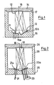
- 11 is an entry pole
- 12 is a concave grating
- 13 is a diode row.
- the three optical components are seated in two housing parts 14 and 15, which are referred to as molded components and which in a preferred embodiment are cylindrical parts with the common axis 16.
- the surfaces 15a and 15b for the gap 11 and the receiver 13 can be produced with turned parts with a finger cutter.
- the moldings like all moldings described later, can also be produced, for example, as injection or molded parts made of suitable materials, such as plastic or metal, or also of glass or ceramic, in particular compacted ceramic.
- the molded body parts 14 and 15 can be assembled in an exactly aligned manner, wherein a security against rotation about the axis 16 is also possible in a known manner.
- the adjustment and permanent fixation of the optical components or their manufacture with exact position and orientation in or on the molded parts will be described later.
- Figure 2 shows a slightly modified embodiment of the structure from molded articles. in which the gap is also replaced by an input optical fiber 21 and the receiver by a plurality of output optical fibers 23, as is known from multiplexers and demultiplexers for fiber optic telecommunications.
- the optical components 21, 12 and 23 are seated here in two molded components 24 and 25, which are connected by the molded spacer 28.
- the three shaped bodies 24, 25, 28 raised a common axis 16 and can also be e.g. inexpensive to manufacture as turned parts with high accuracy.
- the molded molded body 25 is flat and therefore offers advantages for the adjustment and fixing or manufacture of the optical components.
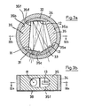
- FIG. 1 Another embodiment is shown in FIG.
- the optical components 11, 12 and 13 are seated on cylindrical segment shaped components 31, 32 and 33, which are arranged in the cylindrical cavity 34. They fill this together with the spacer molding 35 in this way. that the component moldings 31, 32 and 33 can only come in precisely defined boxes.
- Shank shaped body 35 on its outer circumference from the cylinder surfaces 35a and 35b and the segment surfaces 35c, 35d and 35e.
- the shaped shaped body 35 has a sufficiently large recess 35f on the inside for the stray passage of the spectrometer.
- All the moldings are seated on the base plate 38, which is shown in the section shown in FIG. 3b, so that the component moldings 31, 32 and 33 also come to each other at exactly the right height.
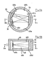
- FIG. 4 A similar embodiment is shown in FIG. 4, in which the shaped molded body 35 from FIG. 3 is superfluous in that the base plate 48 and a cover plate 49 also take over its function. For this purpose, they raised a step-like part on the inside 48i and 49i, which is delimited by the cylinder surfaces 48o and 48b and by the segment surfaces 48c, 48d and 48e.
- the cavity molded part 34 is first placed on the base plate 48, then the molded component parts 31, 32 and 33 are inserted and finally the cover plate 49 is placed on.
- Bottom plot 48 and cover plate 49 can be pressed together in a known manner and, if necessary, fixed on the hollow molded body 34. If - as drawn in FIGS. 3 and 4 - the molded component bodies 31, 32 and 33 raised a small segment height on both sides than at any point in between, then they are immovably fixed in the manner described, as in FIG. 3.
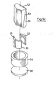
- FIG. 5 shows a particularly advantageous embodiment in which the component moldings are brought into the exactly correct position with respect to one another by adjusting moldings.
- Figure 5c shows a particularly advantageous embodiment in which the component moldings are brought into the exactly correct position with respect to one another by adjusting moldings.
- Figure 5c shows a particularly advantageous embodiment in which the component moldings are brought into the exactly correct position with respect to one another by adjusting moldings.
- Figure 5c shows a particularly advantageous embodiment in which the component moldings are brought into the exactly correct position with respect to one another by adjusting moldings.
- Figure 5c shows a particularly advantageous embodiment in which the component moldings are brought into the exactly correct position with respect to one another by adjusting moldings.
- Figure 5c shows a particularly advantageous embodiment in which the component moldings are brought into the exactly correct position with respect to one another by adjusting moldings.
- Figure 5c shows a particularly advantageous embodiment in which the component moldings are brought into the exactly correct position with respect to one another by adjusting moldings.
- Figure 5c shows a particularly advantageous embodiment
- the fixation of the component molded body to the cavity molded body can e.g. with the connection techniques specified in DE-OS 32 11 867. It is also possible to provide small channels or small plonos from above on the cylinder surfaces of the component moldings (not shown). In the resulting gap between the cavity moldings and component moldings (which can be designed so that they do not affect the flawless system), an adhesive, such as IS 420 from Loctite, which ensures that the connection is permanent. Once the component moldings have been fixed in place, the adjustment moldings are removed again.
- an adhesive such as IS 420 from Loctite
- the optical components In order for the optical components to come into the correct position by assembling the molded parts, they must first be precisely adjusted and fixed to the surfaces that are decisive for the assembly, or they must be produced on the component moldings with an exact position and orientation. In the case of the gap 11, the receiver 13 and the optical fibers 21, 23, the requirements for the accuracy of the adjustment are such that known measuring microscopes are sufficient for the adjustment.
- the radiation to be examined is often fed through an optical fiber; in multiplexers and demultiplexers for fiber optic communication technology, the straw is fed in and out via optical fibers.
- the attachment and adjustment of the optical fibers is suitably started in the following manner: In a ötzbare glass plate (. 21 0 or 23o in Figure 2, for example from Foturon the Fo Schott) of suitable dimensions, one or more holes with possendem diameter is etched more appropriate exposure. The optical fibers are cemented into these holes and then their ends are ground flush with that of the glass plate, the glass plotting being given its desired thickness. Finally, the glass plate with the optical fiber 21 or the optical fibers 23 is adjusted and fixed on the molded body, for example 23, under a measuring microscope.
- the photo layer necessary for producing the grid is then applied to the spherical surface provided for the concave grid using known technology.
- the exposure of this photo layer takes place in a functionally identical arrangement as in the later use of the concave grating.
- the receiver is also replaced by a circular aperture at a calculated location. (The exact position results from an optimization calculation for the respective intended use of the spectrometer.)
- the two circular balls are used as the source points for the production of the holographic grating in a known manner. In this way, a lattice is created on the component molded body, which has the correct position and orientation.
- All materials that can be machined or manufactured with sufficient accuracy e.g. Metal, plastics, glass or ceramics, especially compacted ceramics. Ceramic, glass and plastics have the advantage that no corrosion protection is necessary. Glass and ceramics allow surface qualities that cannot be achieved with metal. Plastics are particularly suitable as injection molded or pressed parts for large quantities if maximum accuracy is not important.
- the described invention is suitable for the production of individual optical devices as well as for the production of large quantities.
Landscapes
- Physics & Mathematics (AREA)
- General Physics & Mathematics (AREA)
- Spectroscopy & Molecular Physics (AREA)
- Optics & Photonics (AREA)
- Engineering & Computer Science (AREA)
- Microelectronics & Electronic Packaging (AREA)
- Optical Couplings Of Light Guides (AREA)
- Diffracting Gratings Or Hologram Optical Elements (AREA)
- Mounting And Adjusting Of Optical Elements (AREA)
- Optical Head (AREA)
- Moving Of The Head For Recording And Reproducing By Optical Means (AREA)
Applications Claiming Priority (2)
| Application Number | Priority Date | Filing Date | Title |
|---|---|---|---|
| DE19853509131 DE3509131A1 (de) | 1985-03-14 | 1985-03-14 | Verfahren zur justierten montage der optischen bauteile eines optischen geraetes |
| DE3509131 | 1985-03-14 |
Publications (2)
| Publication Number | Publication Date |
|---|---|
| EP0194613A2 true EP0194613A2 (fr) | 1986-09-17 |
| EP0194613A3 EP0194613A3 (fr) | 1989-08-30 |
Family
ID=6265182
Family Applications (1)
| Application Number | Title | Priority Date | Filing Date |
|---|---|---|---|
| EP86103084A Withdrawn EP0194613A3 (fr) | 1985-03-14 | 1986-03-07 | Méthode pour le montage de précision des éléments d'un appareil optique |
Country Status (4)
| Country | Link |
|---|---|
| US (1) | US4644632A (fr) |
| EP (1) | EP0194613A3 (fr) |
| JP (1) | JPS61217017A (fr) |
| DE (1) | DE3509131A1 (fr) |
Cited By (8)
| Publication number | Priority date | Publication date | Assignee | Title |
|---|---|---|---|---|
| EP0343290A1 (fr) * | 1984-11-29 | 1989-11-29 | Kaptron Inc. | Construction hybride pour des modules fibre-optiques de télécommunication |
| EP0432842A1 (fr) * | 1989-12-12 | 1991-06-19 | Koninklijke Philips Electronics N.V. | Spectromètre à boîte à fentes |
| EP0591758A1 (fr) * | 1992-09-26 | 1994-04-13 | Forschungszentrum Karlsruhe GmbH | Appareil d'analyse pour plusieurs composants |
| WO1998048307A1 (fr) * | 1997-04-23 | 1998-10-29 | INSTITUT FüR MIKROTECHNIK MAINZ GMBH | Composant optique miniaturise, et mode de fabrication |
| EP1041372A1 (fr) * | 1999-04-01 | 2000-10-04 | Gretag-Macbeth AG | Spectromètre |
| AT408149B (de) * | 1999-12-22 | 2001-09-25 | Scan Messtechnik Gmbh | Spektrometrische sonde |
| DE102005050739A1 (de) * | 2005-10-22 | 2007-04-26 | Esa Patentverwertungsagentur Sachsen-Anhalt Gmbh | Demultiplex-Empfänger für Polymerfaserübertragung und Verfahren zu dessen Herstellung |
| DE102007045668A1 (de) * | 2007-09-25 | 2009-04-02 | Binder-Kontakte Gmbh | Spektrometer mit Eintrittsspalt und die Herstellung des Eintrittsspaltes |
Families Citing this family (27)
| Publication number | Priority date | Publication date | Assignee | Title |
|---|---|---|---|---|
| DE19504834C1 (de) * | 1995-02-14 | 1996-06-13 | Hewlett Packard Gmbh | Diodenzeilen-Spektralphotometer |
| JPH0980300A (ja) * | 1995-09-11 | 1997-03-28 | Asahi Optical Co Ltd | 自動焦点検出用光学ユニット |
| US6548176B1 (en) | 1997-04-03 | 2003-04-15 | The Board Of Trustees Of The Leland Stanford Junior University | Hydroxide-catalyzed bonding |
| JP3677593B2 (ja) * | 1999-03-30 | 2005-08-03 | 日本板硝子株式会社 | 光分波器及びその調心組立方法 |
| DE29906678U1 (de) * | 1999-04-15 | 1999-07-29 | Carl Zeiss Jena Gmbh, 07745 Jena | Spektrometer |
| DE10304312A1 (de) * | 2003-02-04 | 2004-08-12 | Carl Zeiss Jena Gmbh | Kompakt-Spektrometer |
| JP4409860B2 (ja) * | 2003-05-28 | 2010-02-03 | 浜松ホトニクス株式会社 | 光検出器を用いた分光器 |
| US7502109B2 (en) * | 2005-05-17 | 2009-03-10 | Honeywell International Inc. | Optical micro-spectrometer |
| US7678458B2 (en) * | 2007-01-24 | 2010-03-16 | Asml Holding N.V. | Bonding silicon silicon carbide to glass ceramics |
| JP4891841B2 (ja) * | 2007-06-08 | 2012-03-07 | 浜松ホトニクス株式会社 | 分光モジュール |
| KR101503079B1 (ko) | 2007-06-08 | 2015-03-16 | 하마마츠 포토닉스 가부시키가이샤 | 분광기 |
| JP4891840B2 (ja) * | 2007-06-08 | 2012-03-07 | 浜松ホトニクス株式会社 | 分光モジュール |
| US7817274B2 (en) * | 2007-10-05 | 2010-10-19 | Jingyun Zhang | Compact spectrometer |
| WO2009070459A1 (fr) | 2007-11-30 | 2009-06-04 | Jingyun Zhang | Spectromètres miniatures fonctionnant avec des téléphones cellulaires et autres dispositifs électroniques portables |
| JP2009300417A (ja) * | 2008-05-15 | 2009-12-24 | Hamamatsu Photonics Kk | 分光モジュールの製造方法及び分光モジュール |
| JP5205238B2 (ja) * | 2008-05-15 | 2013-06-05 | 浜松ホトニクス株式会社 | 分光モジュール |
| JP5205239B2 (ja) | 2008-05-15 | 2013-06-05 | 浜松ホトニクス株式会社 | 分光器 |
| JP5205242B2 (ja) | 2008-05-15 | 2013-06-05 | 浜松ホトニクス株式会社 | 分光器の製造方法 |
| JP5207938B2 (ja) | 2008-05-15 | 2013-06-12 | 浜松ホトニクス株式会社 | 分光モジュール及び分光モジュールの製造方法 |
| JP5512961B2 (ja) * | 2008-05-15 | 2014-06-04 | 浜松ホトニクス株式会社 | 分光モジュール及びその製造方法 |
| JP2009300422A (ja) * | 2008-05-15 | 2009-12-24 | Hamamatsu Photonics Kk | 分光モジュール |
| JP5415060B2 (ja) | 2008-05-15 | 2014-02-12 | 浜松ホトニクス株式会社 | 分光モジュール |
| JP5205243B2 (ja) * | 2008-05-15 | 2013-06-05 | 浜松ホトニクス株式会社 | 分光器 |
| JP5205240B2 (ja) * | 2008-05-15 | 2013-06-05 | 浜松ホトニクス株式会社 | 分光モジュールの製造方法及び分光モジュール |
| JP5205241B2 (ja) * | 2008-05-15 | 2013-06-05 | 浜松ホトニクス株式会社 | 分光モジュール |
| JP2009300418A (ja) * | 2008-05-15 | 2009-12-24 | Hamamatsu Photonics Kk | 分光モジュール |
| JP2010261767A (ja) * | 2009-05-01 | 2010-11-18 | Canon Inc | 分光装置及びそれを有する画像形成装置 |
Family Cites Families (12)
| Publication number | Priority date | Publication date | Assignee | Title |
|---|---|---|---|---|
| US2535289A (en) * | 1948-02-07 | 1950-12-26 | Hopp Press Inc | Division plate |
| FR1299711A (fr) * | 1961-06-16 | 1962-07-27 | Dispositif pour l'assemblage de lunettes | |
| CA1114795A (fr) * | 1978-03-22 | 1981-12-22 | John Bjorlund | Retroreflecteur de delimitation d'une voie carrossable |
| US4277141A (en) * | 1979-03-28 | 1981-07-07 | Tropel, Inc. | Multifaceted mirror and assembly fixture and method of making such mirror |
| US4259014A (en) * | 1979-04-03 | 1981-03-31 | Princeton Applied Research Corporation | Fiber optic polychromator |
| US4268170A (en) * | 1979-09-18 | 1981-05-19 | Acton Research Corporation | Multi-path monochromator |
| PH17194A (en) * | 1980-03-06 | 1984-06-19 | Otsuka Pharma Co Ltd | Novel carbostyril derivatives,and pharmaceutical composition containing the same |
| US4494872A (en) * | 1980-10-07 | 1985-01-22 | Baylor University | Multiple entrance aperture dispersive optical spectrometer |
| US4387955A (en) * | 1981-02-03 | 1983-06-14 | The United States Of America As Represented By The Secretary Of The Air Force | Holographic reflective grating multiplexer/demultiplexer |
| DE3211867A1 (de) * | 1982-03-31 | 1983-06-01 | Fa. Carl Zeiss, 7920 Heidenheim | Verfahren und vorrichtung zum justieren und montieren von optischen bauteilen in optischen geraeten |
| DE3211868A1 (de) * | 1982-03-31 | 1983-05-26 | Fa. Carl Zeiss, 7920 Heidenheim | Chassis fuer optische geraete |
| US4540282A (en) * | 1983-03-21 | 1985-09-10 | Isaac Landa | Apparatus for optically analyzing a sample |
-
1985
- 1985-03-14 DE DE19853509131 patent/DE3509131A1/de not_active Withdrawn
-
1986
- 1986-03-07 EP EP86103084A patent/EP0194613A3/fr not_active Withdrawn
- 1986-03-13 US US06/839,339 patent/US4644632A/en not_active Expired - Fee Related
- 1986-03-14 JP JP61055193A patent/JPS61217017A/ja active Pending
Cited By (12)
| Publication number | Priority date | Publication date | Assignee | Title |
|---|---|---|---|---|
| EP0343290A1 (fr) * | 1984-11-29 | 1989-11-29 | Kaptron Inc. | Construction hybride pour des modules fibre-optiques de télécommunication |
| EP0432842A1 (fr) * | 1989-12-12 | 1991-06-19 | Koninklijke Philips Electronics N.V. | Spectromètre à boîte à fentes |
| EP0591758A1 (fr) * | 1992-09-26 | 1994-04-13 | Forschungszentrum Karlsruhe GmbH | Appareil d'analyse pour plusieurs composants |
| WO1998048307A1 (fr) * | 1997-04-23 | 1998-10-29 | INSTITUT FüR MIKROTECHNIK MAINZ GMBH | Composant optique miniaturise, et mode de fabrication |
| EP1041372A1 (fr) * | 1999-04-01 | 2000-10-04 | Gretag-Macbeth AG | Spectromètre |
| US6606156B1 (en) | 1999-04-01 | 2003-08-12 | Gretag-Macbeth Ag | Spectrometer |
| AT408149B (de) * | 1999-12-22 | 2001-09-25 | Scan Messtechnik Gmbh | Spektrometrische sonde |
| WO2001046676A3 (fr) * | 1999-12-22 | 2002-02-07 | Scan Messtechnik Gmbh | Sonde spectrometrique |
| DE102005050739A1 (de) * | 2005-10-22 | 2007-04-26 | Esa Patentverwertungsagentur Sachsen-Anhalt Gmbh | Demultiplex-Empfänger für Polymerfaserübertragung und Verfahren zu dessen Herstellung |
| DE102005050739B4 (de) * | 2005-10-22 | 2011-07-07 | ESA Patentverwertungsagentur Sachsen-Anhalt GmbH, 39114 | Demultiplex-Empfänger für Polymerfaserübertragung und Verfahren zu dessen Herstellung |
| DE102007045668A1 (de) * | 2007-09-25 | 2009-04-02 | Binder-Kontakte Gmbh | Spektrometer mit Eintrittsspalt und die Herstellung des Eintrittsspaltes |
| US8102526B2 (en) | 2007-09-25 | 2012-01-24 | Carl Zeiss Microimaging Gmbh | Spectrometer with a slit for incident light and fabrication of the slit |
Also Published As
| Publication number | Publication date |
|---|---|
| DE3509131A1 (de) | 1986-09-18 |
| JPS61217017A (ja) | 1986-09-26 |
| EP0194613A3 (fr) | 1989-08-30 |
| US4644632A (en) | 1987-02-24 |
Similar Documents
| Publication | Publication Date | Title |
|---|---|---|
| EP0194613A2 (fr) | Méthode pour le montage de précision des éléments d'un appareil optique | |
| DE2849975C2 (fr) | ||
| DE3752078T2 (de) | Optischer Stecker | |
| DE3640616A1 (de) | Justiervorrichtung | |
| EP0194612A2 (fr) | Multiplexeur ou démultiplexeur de longueurs d'ondes | |
| DE69011751T2 (de) | Verfahren und Vorrichtung zur Markierung und Spaltung von monokristallinen halbleitenden Plättchen. | |
| EP0990931A2 (fr) | Dispositif de réglage de composants optiques | |
| EP0429877B1 (fr) | Dispositif de positionnement de fibres optiques dans des éléments de connexion | |
| EP1237033A2 (fr) | Mélangeur pour l'intégration de lumière en forme de bâton creux et procédé pour sa fabrication | |
| DE69834870T2 (de) | Ausrichtsystem für einen faseroptischen Steckerstift | |
| DE3032267C2 (fr) | ||
| DE2354338B2 (de) | Vorrichtung zur Montage einer aus Röhrensockel und vormontiertem Mehrstrahlsystem gebildeten Sockeleinheit am Kolben einer Kathodenstrahlröhre | |
| EP0625272B1 (fr) | Procede pour la fabrication d'un couvercle pour un circuit optique integre | |
| DE4423842C2 (de) | Steckverbinder für Lichtwellenleiter und Formeinsatz zur Herstellung desselben | |
| DE2627042A1 (de) | Vorrichtung zur verbindung von lichtleitfaserkabeln | |
| DE69220554T2 (de) | Einstückig gegossene Ausrichthülse für faseroptischen Stecker und ihr Herstellungsverfahren | |
| EP0241684A2 (fr) | Procédé et arrangement pour l'assemblage ajusté des éléments optiques | |
| EP1395859B1 (fr) | Actionneur ajustable à l'aide d'un laser, composant optique et procédé d'ajustage | |
| DE102019120954B4 (de) | Verfahren zur Herstellung einer Klebeverbindung, Trägerplatte für die Herstellung einer Klebeverbindung und Klebevorrichtung zur Herstellung einer Klebeverbindung | |
| DE2705852A1 (de) | Vorrichtung fuer die praezisionsbearbeitung von brillenglasrohlingen | |
| EP0786326A1 (fr) | Procédé et dispositif pour la fabrication de lentilles optiques et feuilles lenticulaires | |
| DE2926003A1 (de) | Vorrichtung und verfahren zur herstellung von teilen eines optischen verzweigerelementes | |
| DE3246358A1 (de) | Vorrichtung zum spielfreien verschieben von objekten in einem koordinatensystem | |
| DE3146026A1 (de) | Abbildungseinrichtung | |
| DE19904445A1 (de) | Linsenstecker zum Aufbau kompakter Freistrahlanordnungen für mehrere Lichtleitfasern |
Legal Events
| Date | Code | Title | Description |
|---|---|---|---|
| PUAI | Public reference made under article 153(3) epc to a published international application that has entered the european phase |
Free format text: ORIGINAL CODE: 0009012 |
|
| AK | Designated contracting states |
Kind code of ref document: A2 Designated state(s): CH DE FR GB IT LI SE |
|
| PUAL | Search report despatched |
Free format text: ORIGINAL CODE: 0009013 |
|
| AK | Designated contracting states |
Kind code of ref document: A3 Designated state(s): CH DE FR GB IT LI SE |
|
| STAA | Information on the status of an ep patent application or granted ep patent |
Free format text: STATUS: THE APPLICATION IS DEEMED TO BE WITHDRAWN |
|
| 18D | Application deemed to be withdrawn |
Effective date: 19891002 |
|
| RIN1 | Information on inventor provided before grant (corrected) |
Inventor name: GLUECK FRANZ Inventor name: BITTNER, REINHOLD Inventor name: SCHLEMMER, HARRY, DR. RER. NAT. Inventor name: SACHSE, RICHARD Inventor name: MAECHLER, MEINRAD |