EP0194613A2 - Verfahren zur justierten Montage der optischen Bauteile eines optischen Gerätes - Google Patents
Verfahren zur justierten Montage der optischen Bauteile eines optischen Gerätes Download PDFInfo
- Publication number
- EP0194613A2 EP0194613A2 EP86103084A EP86103084A EP0194613A2 EP 0194613 A2 EP0194613 A2 EP 0194613A2 EP 86103084 A EP86103084 A EP 86103084A EP 86103084 A EP86103084 A EP 86103084A EP 0194613 A2 EP0194613 A2 EP 0194613A2
- Authority
- EP
- European Patent Office
- Prior art keywords
- component
- moldings
- molded
- optical
- adjustment
- Prior art date
- Legal status (The legal status is an assumption and is not a legal conclusion. Google has not performed a legal analysis and makes no representation as to the accuracy of the status listed.)
- Withdrawn
Links
- 230000003287 optical effect Effects 0.000 title claims abstract description 49
- 238000000034 method Methods 0.000 title claims description 20
- 238000000465 moulding Methods 0.000 claims abstract description 59
- 239000013307 optical fiber Substances 0.000 claims description 13
- 239000011521 glass Substances 0.000 claims description 11
- 238000004519 manufacturing process Methods 0.000 claims description 11
- 239000000919 ceramic Substances 0.000 claims description 8
- 238000003780 insertion Methods 0.000 claims description 5
- 230000037431 insertion Effects 0.000 claims description 5
- 239000004033 plastic Substances 0.000 claims description 5
- 229920003023 plastic Polymers 0.000 claims description 5
- 125000006850 spacer group Chemical group 0.000 claims description 5
- 239000002184 metal Substances 0.000 claims description 4
- 238000005516 engineering process Methods 0.000 description 3
- 239000000835 fiber Substances 0.000 description 3
- 238000002347 injection Methods 0.000 description 2
- 239000007924 injection Substances 0.000 description 2
- 239000000463 material Substances 0.000 description 2
- 239000000853 adhesive Substances 0.000 description 1
- 230000001070 adhesive effect Effects 0.000 description 1
- 230000005540 biological transmission Effects 0.000 description 1
- 238000004364 calculation method Methods 0.000 description 1
- 238000004891 communication Methods 0.000 description 1
- 238000005260 corrosion Methods 0.000 description 1
- 230000007797 corrosion Effects 0.000 description 1
- 239000003292 glue Substances 0.000 description 1
- 239000007788 liquid Substances 0.000 description 1
- 238000005457 optimization Methods 0.000 description 1
- 238000003825 pressing Methods 0.000 description 1
- 230000005855 radiation Effects 0.000 description 1
- 239000010902 straw Substances 0.000 description 1
- 239000000126 substance Substances 0.000 description 1
Images

Classifications
-
- G—PHYSICS
- G02—OPTICS
- G02B—OPTICAL ELEMENTS, SYSTEMS OR APPARATUS
- G02B6/00—Light guides; Structural details of arrangements comprising light guides and other optical elements, e.g. couplings
- G02B6/10—Light guides; Structural details of arrangements comprising light guides and other optical elements, e.g. couplings of the optical waveguide type
- G02B6/12—Light guides; Structural details of arrangements comprising light guides and other optical elements, e.g. couplings of the optical waveguide type of the integrated circuit kind
- G02B6/12007—Light guides; Structural details of arrangements comprising light guides and other optical elements, e.g. couplings of the optical waveguide type of the integrated circuit kind forming wavelength selective elements, e.g. multiplexer, demultiplexer
-
- G—PHYSICS
- G01—MEASURING; TESTING
- G01J—MEASUREMENT OF INTENSITY, VELOCITY, SPECTRAL CONTENT, POLARISATION, PHASE OR PULSE CHARACTERISTICS OF INFRARED, VISIBLE OR ULTRAVIOLET LIGHT; COLORIMETRY; RADIATION PYROMETRY
- G01J3/00—Spectrometry; Spectrophotometry; Monochromators; Measuring colours
- G01J3/02—Details
- G01J3/0256—Compact construction
-
- G—PHYSICS
- G01—MEASURING; TESTING
- G01J—MEASUREMENT OF INTENSITY, VELOCITY, SPECTRAL CONTENT, POLARISATION, PHASE OR PULSE CHARACTERISTICS OF INFRARED, VISIBLE OR ULTRAVIOLET LIGHT; COLORIMETRY; RADIATION PYROMETRY
- G01J3/00—Spectrometry; Spectrophotometry; Monochromators; Measuring colours
- G01J3/02—Details
- G01J3/0291—Housings; Spectrometer accessories; Spatial arrangement of elements, e.g. folded path arrangements
-
- G—PHYSICS
- G02—OPTICS
- G02B—OPTICAL ELEMENTS, SYSTEMS OR APPARATUS
- G02B6/00—Light guides; Structural details of arrangements comprising light guides and other optical elements, e.g. couplings
- G02B6/24—Coupling light guides
- G02B6/42—Coupling light guides with opto-electronic elements
- G02B6/4201—Packages, e.g. shape, construction, internal or external details
- G02B6/4246—Bidirectionally operating package structures
-
- G—PHYSICS
- G02—OPTICS
- G02B—OPTICAL ELEMENTS, SYSTEMS OR APPARATUS
- G02B7/00—Mountings, adjusting means, or light-tight connections, for optical elements
- G02B7/003—Alignment of optical elements
-
- G—PHYSICS
- G02—OPTICS
- G02B—OPTICAL ELEMENTS, SYSTEMS OR APPARATUS
- G02B6/00—Light guides; Structural details of arrangements comprising light guides and other optical elements, e.g. couplings
- G02B6/24—Coupling light guides
- G02B6/26—Optical coupling means
- G02B6/28—Optical coupling means having data bus means, i.e. plural waveguides interconnected and providing an inherently bidirectional system by mixing and splitting signals
- G02B6/293—Optical coupling means having data bus means, i.e. plural waveguides interconnected and providing an inherently bidirectional system by mixing and splitting signals with wavelength selective means
- G02B6/29304—Optical coupling means having data bus means, i.e. plural waveguides interconnected and providing an inherently bidirectional system by mixing and splitting signals with wavelength selective means operating by diffraction, e.g. grating
- G02B6/29305—Optical coupling means having data bus means, i.e. plural waveguides interconnected and providing an inherently bidirectional system by mixing and splitting signals with wavelength selective means operating by diffraction, e.g. grating as bulk element, i.e. free space arrangement external to a light guide
- G02B6/29308—Diffractive element having focusing properties, e.g. curved gratings
-
- Y—GENERAL TAGGING OF NEW TECHNOLOGICAL DEVELOPMENTS; GENERAL TAGGING OF CROSS-SECTIONAL TECHNOLOGIES SPANNING OVER SEVERAL SECTIONS OF THE IPC; TECHNICAL SUBJECTS COVERED BY FORMER USPC CROSS-REFERENCE ART COLLECTIONS [XRACs] AND DIGESTS
- Y10—TECHNICAL SUBJECTS COVERED BY FORMER USPC
- Y10T—TECHNICAL SUBJECTS COVERED BY FORMER US CLASSIFICATION
- Y10T29/00—Metal working
- Y10T29/49—Method of mechanical manufacture
- Y10T29/49826—Assembling or joining
- Y10T29/49904—Assembling a subassembly, then assembling with a second subassembly
Definitions
- the invention relates to a method for the adjusted assembly of the optical components of an optical device.
- the invention also relates to an optical device for performing the method.
- Optical devices consist of several optical components that have to be adjusted exactly to each other or to a chassis so that the tanning has the desired properties. That is why the optical components, e.g. with a spectrometer spolt, grating and receiver, usually with adjustable holders on a device techossis or a similar device. Such Holters are still the number of degrees of freedom that are necessary for adjustment, their structure quite complex and therefore expensive. They also take up space.
- the present invention is therefore based on the object of specifying a method by means of which the components of an optical device which has a volume of the order of ml or less can be adjusted and assembled or assembled and adjusted.
- the invention also has the task of specifying an optical device for carrying out the method.
- optical components are either adjusted and permanently fixed in or on component moldings or are produced with an exact position and orientation, and that the component moldings are then assembled and fixed in a defined manner.
- the optical device is composed of individual parts - referred to here as shaped bodies - which are produced on the contact surfaces which are decisive for the assembly with such accuracy that they fit together positively without play.
- These moldings contain the optical components with the necessary exact position and orientation in relation to the contact surfaces that are decisive for the assembly.
- the component moldings are connected to one another by one or more spacer moldings.
- the component moldings are inserted into a cavity molding.
- the molded component bodies are brought into the exactly correct position relative to one another within the molded cavity body by one or more molded spacers.
- the cavity molding is closed by a base plate and a cover plate. which, together with the cavity molded body, accommodate the component molded bodies in the exactly correct position relative to one another.
- the component moldings are brought into the exactly correct position with respect to one another by means of adjustment moldings, the adjustment moldings being removed after the component moldings are fixed to the cavity moldings.
- a measuring microscope is generally sufficient as an aid for the exact adjustment of the optical components on or in the component moldings in relation to the account areas which are decisive for the assembly of the moldings.
- this method is not sufficient for a number of applications.
- a hologrophic lattice is generated directly on the component molded body, which is arranged under functionally identical conditions to the entrance slit and to the plane of the receiver in later use, the location of the entrance slit or a conjugated location and a suitable point be used as source points for the generation of the grid in the plane of the receiver.
- one of the source points can also be located a small amount next to the location of the entry point.
- 11 is an entry pole
- 12 is a concave grating
- 13 is a diode row.
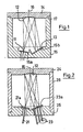
- the three optical components are seated in two housing parts 14 and 15, which are referred to as molded components and which in a preferred embodiment are cylindrical parts with the common axis 16.
- the surfaces 15a and 15b for the gap 11 and the receiver 13 can be produced with turned parts with a finger cutter.
- the moldings like all moldings described later, can also be produced, for example, as injection or molded parts made of suitable materials, such as plastic or metal, or also of glass or ceramic, in particular compacted ceramic.
- the molded body parts 14 and 15 can be assembled in an exactly aligned manner, wherein a security against rotation about the axis 16 is also possible in a known manner.
- the adjustment and permanent fixation of the optical components or their manufacture with exact position and orientation in or on the molded parts will be described later.
- Figure 2 shows a slightly modified embodiment of the structure from molded articles. in which the gap is also replaced by an input optical fiber 21 and the receiver by a plurality of output optical fibers 23, as is known from multiplexers and demultiplexers for fiber optic telecommunications.
- the optical components 21, 12 and 23 are seated here in two molded components 24 and 25, which are connected by the molded spacer 28.
- the three shaped bodies 24, 25, 28 raised a common axis 16 and can also be e.g. inexpensive to manufacture as turned parts with high accuracy.
- the molded molded body 25 is flat and therefore offers advantages for the adjustment and fixing or manufacture of the optical components.
- FIG. 1 Another embodiment is shown in FIG.
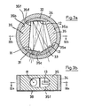
- the optical components 11, 12 and 13 are seated on cylindrical segment shaped components 31, 32 and 33, which are arranged in the cylindrical cavity 34. They fill this together with the spacer molding 35 in this way. that the component moldings 31, 32 and 33 can only come in precisely defined boxes.
- Shank shaped body 35 on its outer circumference from the cylinder surfaces 35a and 35b and the segment surfaces 35c, 35d and 35e.
- the shaped shaped body 35 has a sufficiently large recess 35f on the inside for the stray passage of the spectrometer.
- All the moldings are seated on the base plate 38, which is shown in the section shown in FIG. 3b, so that the component moldings 31, 32 and 33 also come to each other at exactly the right height.
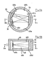
- FIG. 4 A similar embodiment is shown in FIG. 4, in which the shaped molded body 35 from FIG. 3 is superfluous in that the base plate 48 and a cover plate 49 also take over its function. For this purpose, they raised a step-like part on the inside 48i and 49i, which is delimited by the cylinder surfaces 48o and 48b and by the segment surfaces 48c, 48d and 48e.
- the cavity molded part 34 is first placed on the base plate 48, then the molded component parts 31, 32 and 33 are inserted and finally the cover plate 49 is placed on.
- Bottom plot 48 and cover plate 49 can be pressed together in a known manner and, if necessary, fixed on the hollow molded body 34. If - as drawn in FIGS. 3 and 4 - the molded component bodies 31, 32 and 33 raised a small segment height on both sides than at any point in between, then they are immovably fixed in the manner described, as in FIG. 3.
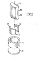
- FIG. 5 shows a particularly advantageous embodiment in which the component moldings are brought into the exactly correct position with respect to one another by adjusting moldings.
- Figure 5c shows a particularly advantageous embodiment in which the component moldings are brought into the exactly correct position with respect to one another by adjusting moldings.
- Figure 5c shows a particularly advantageous embodiment in which the component moldings are brought into the exactly correct position with respect to one another by adjusting moldings.
- Figure 5c shows a particularly advantageous embodiment in which the component moldings are brought into the exactly correct position with respect to one another by adjusting moldings.
- Figure 5c shows a particularly advantageous embodiment in which the component moldings are brought into the exactly correct position with respect to one another by adjusting moldings.
- Figure 5c shows a particularly advantageous embodiment in which the component moldings are brought into the exactly correct position with respect to one another by adjusting moldings.
- Figure 5c shows a particularly advantageous embodiment in which the component moldings are brought into the exactly correct position with respect to one another by adjusting moldings.
- Figure 5c shows a particularly advantageous embodiment
- the fixation of the component molded body to the cavity molded body can e.g. with the connection techniques specified in DE-OS 32 11 867. It is also possible to provide small channels or small plonos from above on the cylinder surfaces of the component moldings (not shown). In the resulting gap between the cavity moldings and component moldings (which can be designed so that they do not affect the flawless system), an adhesive, such as IS 420 from Loctite, which ensures that the connection is permanent. Once the component moldings have been fixed in place, the adjustment moldings are removed again.
- an adhesive such as IS 420 from Loctite
- the optical components In order for the optical components to come into the correct position by assembling the molded parts, they must first be precisely adjusted and fixed to the surfaces that are decisive for the assembly, or they must be produced on the component moldings with an exact position and orientation. In the case of the gap 11, the receiver 13 and the optical fibers 21, 23, the requirements for the accuracy of the adjustment are such that known measuring microscopes are sufficient for the adjustment.
- the radiation to be examined is often fed through an optical fiber; in multiplexers and demultiplexers for fiber optic communication technology, the straw is fed in and out via optical fibers.
- the attachment and adjustment of the optical fibers is suitably started in the following manner: In a ötzbare glass plate (. 21 0 or 23o in Figure 2, for example from Foturon the Fo Schott) of suitable dimensions, one or more holes with possendem diameter is etched more appropriate exposure. The optical fibers are cemented into these holes and then their ends are ground flush with that of the glass plate, the glass plotting being given its desired thickness. Finally, the glass plate with the optical fiber 21 or the optical fibers 23 is adjusted and fixed on the molded body, for example 23, under a measuring microscope.
- the photo layer necessary for producing the grid is then applied to the spherical surface provided for the concave grid using known technology.
- the exposure of this photo layer takes place in a functionally identical arrangement as in the later use of the concave grating.
- the receiver is also replaced by a circular aperture at a calculated location. (The exact position results from an optimization calculation for the respective intended use of the spectrometer.)
- the two circular balls are used as the source points for the production of the holographic grating in a known manner. In this way, a lattice is created on the component molded body, which has the correct position and orientation.
- All materials that can be machined or manufactured with sufficient accuracy e.g. Metal, plastics, glass or ceramics, especially compacted ceramics. Ceramic, glass and plastics have the advantage that no corrosion protection is necessary. Glass and ceramics allow surface qualities that cannot be achieved with metal. Plastics are particularly suitable as injection molded or pressed parts for large quantities if maximum accuracy is not important.
- the described invention is suitable for the production of individual optical devices as well as for the production of large quantities.
Landscapes
- Physics & Mathematics (AREA)
- General Physics & Mathematics (AREA)
- Spectroscopy & Molecular Physics (AREA)
- Optics & Photonics (AREA)
- Engineering & Computer Science (AREA)
- Microelectronics & Electronic Packaging (AREA)
- Optical Couplings Of Light Guides (AREA)
- Mounting And Adjusting Of Optical Elements (AREA)
- Diffracting Gratings Or Hologram Optical Elements (AREA)
- Moving Of The Head For Recording And Reproducing By Optical Means (AREA)
- Optical Head (AREA)
Abstract
Description
- Die Erfindung betrifft ein Verfahren zur justierten Montage der optischen Bauteile eines optischen Gerötes. Die Erfindung betrifft außerdem ein optisches Gerät zur Durchführung des Verfahrens.
- Optische Geröte bestehen aus mehreren optischen Bauteilen, die genau zueinander bzw. zu einem Chassis justiert sein müssen, damit das Gerbt die gewünschten Eigenschaften hot. Deswegen sind die optischen Bauteile, wie z.B. bei einem Spektrometer Spolt, Gitter und Empfänger, meist mit justierboren Haltern auf einem Gerä techossis oder einer ähnlichen Einrichtung ongeordnet. Derartige Holter sind je noch der Zahl der Freiheitsgrade, die zum Justieren notwendig sind, in ihrem Aufbau recht aufwendig und damit teuer. Außerdem beanspruchen sie Platz.
- Aus der DE-OS 32 11 867 ist bekannt, beim Justieren und Montieren eines optischen Bauteiles in einem optischen Gerät das optische Bauteil von einer nicht zum Gerät gehörenden Justiervorrichtung zu halten und mit dieser zu justieren und es noch dem Justiervorgang mit dem Gerät durch eine flüssige oder pastenförmige Substanz, welche sich mit geringer Volumenänderung verfestigt, zu verbinden und später die Justiervorrichtung zu entfernen. Auf diese Weise wird ein platzsparender Aufbau des optischen Gerätes erreicht und die Halterung der optischen Bauteile ist sehr einfach und damit preiswert.
- Ein Nachteil dieses Verfahrens ist, daß die Justiervorrichtungen während des Montage- und Justagevorganges Platz beanspruchen und es daher bei optischen Geräten, die ein sehr kleines Volumen hoben, nur noch mit erheblichen Schwierigkeiten oder gar nicht mehr angewendet werden kann. In jüngster Zeit hoben aber z.B. Spektrometer, deren Volumen in der Größenordnung von ml oder darunter liegt, zunehmend an Bedeutung gewonnen. Auch bei anderen optischen Geräten ist seit einiger Zeit eine Tendenz zur Miniaturisierung vorhanden. Das gilt besonders bei Multiplexern und Demultiplexern für die faseroptische Nachrichtenübertragung.
- Der vorliegenden Erfindung liegt daher die Aufgabe zugrunde, ein Verfahren anzugeben, mit der die Bauelemente eines optischen Gerätes, das ein Volumen in der Größenordnung von ml oder weniger hat, justiert und montiert bzw. montiert und justiert werden können. Die Erfindung hat ferner die Aufgabe, ein optisches Gerät zur Durchführung des Verfahrens anzugeben.
- Die gestellte Aufgabe wird erfindungsgemäß dadurch gelöst, daß die optischen Bauteile in bzw. auf Bauteilformkörpern entweder justiert und dauerhaft fixiert oder mit genauer Lage und Ausrichtung hergestellt werden und daß anschließend die Bauteilformkörper in definierter Weise zusammengesetzt und fixiert werden.
- Im Gegensatz zum bekannten Stand der Technik wird also das optische Gerät aus einzelnen Teilen - hier als Formkörper bezeichnet - zusammengesetzt, welche an den für das Zusammensetzen maßgebenden Kontaktflöchen mit solcher Genauigkeit hergestellt werden, daß sie ohne Spiel formschlüssig zusammenpassen. Diese Formkörper enthalten die optischen Bauteile mit der notwendigen genauen Lage und Ausrichtung in Bezug auf die für das Zusammensetzen maßgebenden Kontaktflöchen.
- In einer vorteilhaften Ausgestaltung der Erfindung werden die Bauteilformkörper durch einen oder mehrere Abstandsformkörper miteinander verbunden.
- In einer anderen vorteilhaften Ausführungsform der Erfindung werden die Bauteilformkörper in einen Hohlraumformkörper eingesetzt. Dabei werden in einer Ausgestaltung die Bauteilformkörper durch ein oder mehrere Abstandsformkörper in die exakt richtige Lage zueinander innerhalb des Hohlraumformkörpers gebracht. In einer anderen Ausgestaltung wird der Hohlraumformkörper durch eine Bodenplatte und eine Deckplatte verschlossen. die zusammen mit dem Hohlraumformkörper die Bauteilformkörper in der exakt richtigen Lage zueinander aufnehmen. In einer weiteren, besonders vorteilhaften Ausgestaltung werden die Bauteilformkörper innerhalb des Hohlraumformkörpers durch Justierformkörper in die exakt richtige Lage zueinander gebracht, wobei die Justierformkörper entfernt werden, nachdem die Bauteilformkörper am Hohlraumformkörper fixiert sind.
- Für die genaue Justierung der optischen Bauteile auf bzw. in den Bauteilformkörpern in Bezug auf die für das Zusammensetzen der Formkörper maßgebenden Kontoktflöchen reicht im allgemeinen als Hilfsmittel ein Meßmikroskop. Für ein Konkavgitter ist diese Methode jedoch für eine Reihe von Anwendungsföllen nicht ausreichend. In einer vorteilhaften Ausgestaltung der Erfindung wird daher ein hologrophisches Gitter unmittelbar auf dem Bauteilformkörper erzeugt, der unter funktionsgleichen Bedingungen wie bei der späteren Verwendung zum Eintrittsspalt und zur Ebene des Empfängers angeordnet ist, wobei der Ort des Eintrittsspaltes oder ein dazu konjugierter Ort und ein geeigneter Punkt in der Ebene des Empföngers als Quellpunkte für die Erzeugung des Gitters verwendet werden. Für eine optimale Korrektur kann einer der Quellpunkte auch um einen kleinen Betrag neben dem Ort des Eintrittsspoltes liegen.
- Es ist auch möglich. z.B. den Eintrittsspolt oder Lichtleitfaseranschlüsse unmittelbar in einem Bauteilformkörper herzustellen.
- Weitere Ausgestaltungen der Erfindung gehen aus den Unteransprüchen hervor.
- .Die Erfindung eignet sich ganz allgemein für optische Geröte. Sie wird im folgenden anhand von in den Figuren 1 bis 5 mit vergrößertem Maßstab dargestellten Ausführungsbeispielen für ein Spektrometer und einen Multiplexer/Demultiplexer näher erläutert. Dabei zeigen
- Fig. 1 ein erstes Ausführungsbeispiel für ein Spektrometer;
- Fig. 2 ein Ausführungsbeispiel für einen Multiplexer/Demultiplexer;
- Fig. 3a,b ein zweites Ausführungsbeispiel für ein Spektrometer;
- Fig. 4a,b ein drittes Ausführungsbeispiel für ein Spektrometer und
- Fig. 5a-c ein viertes Ausführungsbeispiel für ein Spektrometer.
- In Figur 1 ist mit 11 ein Eintrittsspolt, mit 12 ein Konkavgitter und mit 13 eine Diodenzeile bezeichnet. Diese drei optischen Bauteile bilden eine bekannte Spektrometeronordnung, die sog. Rowlandanordnung. Die drei optischen Bauteile sitzen in zwei Gehäuseteilen 14 und 15, die als Bauteilformkörper bezeichnet werden und die in einer bevorzugten Ausführungsform zylindrische Teile mit der gemeinsamen Achse 16 sind. Die Flachen 15a und 15b für den Spalt 11 und den Empfönger 13 können bei Drehteilen mit einem Fingerfröser hergestellt werden. Die Formkörper können jedoch ebenso wie alle spöter beschriebenen Formkörper z.B. auch als Spritz- oder Preßgußteile aus geeigneten Materialien, wie z.B. Kunststoff oder Metall, oder auch aus Glas oder Keramik, insbesondere verdichteter Keramik hergestellt werden.
- Durch die Stufe 17 lassen sich die Bouteilformkörper 14 und 15 exakt fluchtend zusammensetzen, wobei auch eine Sicherung gegen Verdrehung um die Achse 16 in bekannter Weise möglich ist. Die Justierung und dauerhofte Fixierung der optischen Bauteile oder deren Herstellung mit genauer Lage und Ausrichtung in bzw. auf den Bouteilformkörpern wird später beschrieben.
- Figur 2 zeigt eine etwas abgeänderte Ausführungsform des Aufbaus aus Formkörpern. bei dem außerdem der Spalt durch eine Eingangslichtleitfaser 21 und der Empfänger durch mehrere Ausgangslichtleitfasern 23 ersetzt sind, wie das von Multiplexern und Demultiplexern für die faseroptische Nachrichtentechnik bekannt ist. Die optischen Bauteile 21, 12 und 23 sitzen hier in zwei Bauteilformkörpern 24 und 25, welche durch den Abstandsformkörper 28 verbunden werden. Die drei Formkörper 24, 25, 28 hoben eine gemeinsame Achse 16 und lassen sich ebenfalls z.B. als Drehteile preiswert mit hoher Genauigkeit herstellen. Gegenüber der in Figur 1 dargestellten Ausführungsform ist der Bouteilformkörper 25 flach und bietet daher für die Justierung und Fixierung oder Herstellung der optischen Bauteile Vorteile.
- In Figur 3 ist eine weitere Ausführungsform dargestellt. Hier sitzen die optischen Bauteile 11, 12 und 13 auf zylindersegmentförmigen Bauteilformkörpern 31, 32 und 33, welche in dem zylinderförmigen Hohlraumformkörper 34 angeordnet sind. Dabei füllen sie diesen zusammen mit dem Abstandsformkörper 35 derart aus. daß die Bauteilformkörper 31, 32 und 33 nur in genau definierte Logen kommen können. Hierfür besteht der Abstondsformkörper 35 an seinem öußeren Umfang aus den Zylinderflächen 35a und 35b und den Segmentflöchen 35c, 35d und 35e. Selbstverständlich hat der Abstondsformkörper 35 innen eine genügend große Aussparung 35f für den Strohlengang des Spektrometers. Alle Formkörper sitzen ouf der Grundplatte 38 auf, welche in dem in Figur 3b gezeigten Schnitt dargestellt ist, so daß die Bauteilformkörper 31, 32 und 33 auch exakt in die richtige Höhe zueinander kommen.
- In Figur 4 ist eine ähnliche Ausführungsform dargestellt, bei welcher der Abstondsformkörper 35 von Figur 3 dadurch überflüssig wird, daß die Bodenplatte 48 und eine Deckplatte 49 seine Funktion mit übernehmen. Sie hoben dazu jeweils auf der Innenseite 48i bzw. 49i einen stufenartigen Teil, welcher durch die Zylinderflächen 48o und 48b und durch die Segmentflöchen 48c, 48d und 48e begrenzt wird. Beim Zusammenbau wird zunächst das Hohlraumformteil 34 auf die Grundplatte 48 gesetzt, dann werden die Bauteilformteile 31, 32 und 33 eingesetzt und schließlich wird die Deckplatte 49 aufgesetzt. Bodenplotte 48 und Deckplatte 49 können auf bekannte Art zusammengepreßt und gegebenenfalls on dem Hohlroumformkörper 34 fixiert werden. Wenn - wie in den·Figuren 3 und 4 gezeichnet - die Bauteilformkörper 31, 32 und 33 an beiden Seiten eine geringe Segmenthöhe hoben als an einer beliebigen Stelle dazwischen, dann sitzen sie in der beschriebenen Weise ebenso wie in Figur 3 unverrückbar fest.
- Figur 5 zeigt eine besonders vorteilhafte Ausführungsform, bei der die Bauteilformkörper durch Justierformkörper in die exakt richtige Lage zueinander gebracht werden. Dies ist in Figur 5c in einer Explosionszeichnung dargestellt. Mit 31, 32 und 33 sind wieder die Bauelementformkörper bezeichnet und mit 34 der zylinderförmige Hohlraumformkörper. Letzterer wird mindestens während des Justiervorganges für die Bauteilformkörper auf die Bodenplatte 38 aufgesetzt. Anschließend werden die Bauteilformkörper 31, 32 und 33 in den Hohlraumformkörper ungefähr an die richtigen Stellen eingesetzt. Danach wird zunächst der Justierformkörper 51 und schließlich der Justierformkörper 52 in den Hohlraumformkörper 34 eingesetzt. Die beiden Justierformkörper haben korrespondierende Keilflächen 53, auf denen sie gegeneinander verschiebbor sind. Der zweite Justierformkörper 52 wird daher noch dem Einsetzen so weit wie möglich noch unten gedrückt. Dadurch erholten die drei Bouteilformkörper exakt die richtige Lage zueinander. Bei dieser Ausführungsform müssen natürlich die optischen Bauteile 11, 12 und 13 versenkt in den Bauteilformkörpern 31, 32 und 33 angeordnet sein.
- Die Fixierung der Bauteilformkörper am Hohlraumformkörper kann z.B. mit den in der DE-OS 32 11 867 angegebenen Verbindungstechniken erfolgen. Es ist auch möglich, an den Zylinderflächen der Bauteilformkörper (nicht gezeichnete) kleine Kanäle oder kleine Plonflöchen von oben noch unten vorzusehen. In die dadurch entstehenden Spalte zwischen Hohlraumformkörper und Bauteilformkörpern (welche so ausgebildet werden können, daß sie die einwandfreie Anlage nicht beeinflussen) kann dann ein Klebemittel, wie z.B. IS 420 der Fa. Loctite eingebracht werden, das noch dem Ausförten für eine dauerhafte Verbindung sorgt. Noch der Fixierung der Bauteilformkörper om Hohlroumformkörper werden die Justierformkörper wieder entfernt.
- Bei den in den Figuren 1 bis 4 dargestellten Ausführungsbeispielen ist das normale Zusammensetzen ausreichend. Der Zusammenhalt der Formteile untereinander kann auf bekannte Weise durch Zusammendrücken in Richtung der Achse 16 oder durch andere bekannte Verbindungstechniken erfolgen.
- Damit die optischen Bauteile durch das Zusammensetzen der Formteile exakt in die richtige Lage kommen, müssen sie vorher exakt zu den für das Zusammensetzen maßgebenden Flachen justiert und fixiert werden bzw. auf den Bauteilformteilen mit genauer Lage und Ausrichtung hergestellt werden. Bei dem Spalt 11, dem Empfänger 13 und den Lichtleitfasern 21, 23 sind die Anforderungen an die Genauigkeit der Justierung so, daß zum Justieren bekannte Meßmikroskope ausreichen.
- Es ist zweckmäßig, die freie Öffnung des Spaltes in einem dünnen Blech vorzusehen und dieses Blech dann auf dem Bauteilformkörper zu justieren. Anschließend kann das Blech auf bekannte Weise fixiert werden, z.B. durch einige Tropfen eines geeigneten Klebers an seinem Rand. Auf die gleiche Weise wird der Empfänger 13, z.B. eine Diodenzeile, auf dem entsprechenden Bauteilformkörper justiert und fixiert.
- Bei Spektrometern wird die zu untersuchende Strahlung häufig durch eine Lichtleitfaser zugeführt; bei Multiplexern und Demultiplexern für die faseroptische Nachrichtentechnik erfolgen Zu- und Abführung der Strohlung über Lichtleitfasern. Die Befestigung und Justierung der Lichtleitfasern erfolgt dann zweckmäßig auf folgende Weise: In eine ötzbare Glasplatte (210 oder 23o in Figur 2, z.B. aus Foturon der Fo. Schott) mit geeigneten Abmessungen werden ein oder mehrere Bohrungen mit possendem Durchmesser noch entsprechender Belichtung eingeätzt. In diese Bohrungen werden die Lichtleitfasern eingekittet und anschließend werden ihre Enden mit der der Glasplatte bündig abgeschliffen, wobei die Glasplotte ihre Solldicke erhält. Schließlich wird die Glasplatte mit der Lichtleitfaser 21 bzw. den Lichtleitfasern 23 unter einem Meßmikroskop auf dem Bouteilformkörper z.B. 23 justiert und fixiert.
- Für dos Konkavgitter ist die Justierung mit einem Meßmikroskop für eine Reihe von Anwendungsfällen nicht ausreichend, da hier eine sehr genaue Ausrichtung notwendig ist. In diesen Föllen kann ein Verfahren verwendet werden, welches die Tatsache ausnutzt, daß bei der Herstellung von holographischen Konkavgitteroriginalen geringere Toleranzen und Kosten anfallen als bei der Herstellung von Kopien. Die Fläche eines Bauteilformkörpers. welcher das Konkavgitter erholten soll, läßt sich mit bekannter Technik als Kugelflöche mit der notwendigen Genauigkeit herstellen. Dies gilt auch für die Orientierung dieser Kugelflöche zu den anderen Flöchen, die für dos Zusammensetzen mit den übrigen Formkörpern maßgebend sind.
- Auf die für das Konkovgitter vorgesehene Kugelfläche wird dann in bekannter Technik die zur Herstellung des Gitters notwendige Photoschicht aufgebracht. Die Belichtung dieser Photoschicht erfolgt in einer funktionsgleichen Anordnung wie bei der spöteren Verwendung des Konkavgitters. Bei dieser Anordnung wird lediglich der Spalt - falls er nicht kreisförmig ist und den richtigen Durchmesser hot - durch eine kreisförmige Blende von z.B. 5 µm Durchmesser ersetzt. Auch der Empfänger wird durch eine kreisförmige Blende an einem berechneten Ort ersetzt. (Die genaue Lage ergibt sich aus einer Optimierungsrechnung für den jeweiligen Verwendungszweck des Spektrometers.) Die beiden kreisförmigen Blenden werden als Quellpunkte für die in bekannter Weise durchgeführte Herstellung des holographischen Gitters verwendet. Auf diese Weise wird auf dem Bauteilformkörper ein Gitter erzeugt, das exakt die richtige Lage und Ausrichtung hat.
- Als Material für die Formkörper kommen alle Werkstoffe in Betracht, die sich mit ausreichender Genauigkeit bearbeiten oder herstellen lassen, also z.B. Metall, Kunststoffe, Glas oder Keramik, insbesondere verdichtete Keramik. Dabei haben Keramik, Glas und Kunststoffe den Vorteil, daß kein Korrosionsschutz notwendig ist. Glas und Keramik erlauben Oberflachengüten, die sich mit Metall nicht erreichen lassen. Kunststoffe sind als Spritzguß- oder Preßteile besonders für große Stückzahlen geeignet, wenn es nicht auf höchste Genauigkeit ankommt.
- Es ist zweckmäßig, den einzelnen Formkörpern solche Formen zu geben, daß sie mit hoher Genauigkeit in den entscheidenden Abmessungen verhältnismäßig preiswert hergestellt werden können. Das ist besonders bei dem Hohlraumformkörper 34 und bei den zylindersegmentförmigen Bauteilformkörpern 31. 32 und 33 der Fall. es gilt ober auch für die in den anderen Figuren gezeigten Formkörper.
- Die beschriebene Erfindung eignet sich sowohl für die Herstellung von einzelnen optischen Geräten als auch für die Herstellung von großen Stückzahlen.
Claims (11)
Applications Claiming Priority (2)
| Application Number | Priority Date | Filing Date | Title |
|---|---|---|---|
| DE19853509131 DE3509131A1 (de) | 1985-03-14 | 1985-03-14 | Verfahren zur justierten montage der optischen bauteile eines optischen geraetes |
| DE3509131 | 1985-03-14 |
Publications (2)
| Publication Number | Publication Date |
|---|---|
| EP0194613A2 true EP0194613A2 (de) | 1986-09-17 |
| EP0194613A3 EP0194613A3 (de) | 1989-08-30 |
Family
ID=6265182
Family Applications (1)
| Application Number | Title | Priority Date | Filing Date |
|---|---|---|---|
| EP86103084A Withdrawn EP0194613A3 (de) | 1985-03-14 | 1986-03-07 | Verfahren zur justierten Montage der optischen Bauteile eines optischen Gerätes |
Country Status (4)
| Country | Link |
|---|---|
| US (1) | US4644632A (de) |
| EP (1) | EP0194613A3 (de) |
| JP (1) | JPS61217017A (de) |
| DE (1) | DE3509131A1 (de) |
Cited By (8)
| Publication number | Priority date | Publication date | Assignee | Title |
|---|---|---|---|---|
| EP0343290A1 (de) * | 1984-11-29 | 1989-11-29 | Kaptron Inc. | Hybrid-Aufbau für faseroptische Kommunikationsbausteine |
| EP0432842A1 (de) * | 1989-12-12 | 1991-06-19 | Koninklijke Philips Electronics N.V. | Spektrometer mit Schlitzenkassette |
| EP0591758A1 (de) * | 1992-09-26 | 1994-04-13 | Forschungszentrum Karlsruhe GmbH | Mehrkomponenten-Analysengerät |
| WO1998048307A1 (de) * | 1997-04-23 | 1998-10-29 | INSTITUT FüR MIKROTECHNIK MAINZ GMBH | Miniaturisiertes optisches bauelement sowie verfahren zu seiner herstellung |
| EP1041372A1 (de) * | 1999-04-01 | 2000-10-04 | Gretag-Macbeth AG | Spektrometer |
| AT408149B (de) * | 1999-12-22 | 2001-09-25 | Scan Messtechnik Gmbh | Spektrometrische sonde |
| DE102005050739A1 (de) * | 2005-10-22 | 2007-04-26 | Esa Patentverwertungsagentur Sachsen-Anhalt Gmbh | Demultiplex-Empfänger für Polymerfaserübertragung und Verfahren zu dessen Herstellung |
| DE102007045668A1 (de) * | 2007-09-25 | 2009-04-02 | Binder-Kontakte Gmbh | Spektrometer mit Eintrittsspalt und die Herstellung des Eintrittsspaltes |
Families Citing this family (27)
| Publication number | Priority date | Publication date | Assignee | Title |
|---|---|---|---|---|
| DE19504834C1 (de) * | 1995-02-14 | 1996-06-13 | Hewlett Packard Gmbh | Diodenzeilen-Spektralphotometer |
| JPH0980300A (ja) * | 1995-09-11 | 1997-03-28 | Asahi Optical Co Ltd | 自動焦点検出用光学ユニット |
| US6548176B1 (en) | 1997-04-03 | 2003-04-15 | The Board Of Trustees Of The Leland Stanford Junior University | Hydroxide-catalyzed bonding |
| JP3677593B2 (ja) * | 1999-03-30 | 2005-08-03 | 日本板硝子株式会社 | 光分波器及びその調心組立方法 |
| DE29906678U1 (de) * | 1999-04-15 | 1999-07-29 | Carl Zeiss Jena Gmbh, 07745 Jena | Spektrometer |
| DE10304312A1 (de) * | 2003-02-04 | 2004-08-12 | Carl Zeiss Jena Gmbh | Kompakt-Spektrometer |
| JP4409860B2 (ja) * | 2003-05-28 | 2010-02-03 | 浜松ホトニクス株式会社 | 光検出器を用いた分光器 |
| US20100239436A1 (en) * | 2005-05-17 | 2010-09-23 | Honeywell International Inc. | A thermal pump |
| US7678458B2 (en) | 2007-01-24 | 2010-03-16 | Asml Holding N.V. | Bonding silicon silicon carbide to glass ceramics |
| CN102519589B (zh) | 2007-06-08 | 2014-10-29 | 浜松光子学株式会社 | 分光器 |
| JP4891841B2 (ja) * | 2007-06-08 | 2012-03-07 | 浜松ホトニクス株式会社 | 分光モジュール |
| JP4891840B2 (ja) * | 2007-06-08 | 2012-03-07 | 浜松ホトニクス株式会社 | 分光モジュール |
| US7817274B2 (en) * | 2007-10-05 | 2010-10-19 | Jingyun Zhang | Compact spectrometer |
| US8345226B2 (en) | 2007-11-30 | 2013-01-01 | Jingyun Zhang | Spectrometers miniaturized for working with cellular phones and other portable electronic devices |
| JP5205239B2 (ja) * | 2008-05-15 | 2013-06-05 | 浜松ホトニクス株式会社 | 分光器 |
| JP5415060B2 (ja) | 2008-05-15 | 2014-02-12 | 浜松ホトニクス株式会社 | 分光モジュール |
| JP5205243B2 (ja) * | 2008-05-15 | 2013-06-05 | 浜松ホトニクス株式会社 | 分光器 |
| JP5205241B2 (ja) * | 2008-05-15 | 2013-06-05 | 浜松ホトニクス株式会社 | 分光モジュール |
| JP2009300417A (ja) * | 2008-05-15 | 2009-12-24 | Hamamatsu Photonics Kk | 分光モジュールの製造方法及び分光モジュール |
| JP5207938B2 (ja) | 2008-05-15 | 2013-06-12 | 浜松ホトニクス株式会社 | 分光モジュール及び分光モジュールの製造方法 |
| JP5205238B2 (ja) * | 2008-05-15 | 2013-06-05 | 浜松ホトニクス株式会社 | 分光モジュール |
| JP2009300418A (ja) * | 2008-05-15 | 2009-12-24 | Hamamatsu Photonics Kk | 分光モジュール |
| JP2009300422A (ja) * | 2008-05-15 | 2009-12-24 | Hamamatsu Photonics Kk | 分光モジュール |
| JP5205240B2 (ja) * | 2008-05-15 | 2013-06-05 | 浜松ホトニクス株式会社 | 分光モジュールの製造方法及び分光モジュール |
| JP5205242B2 (ja) * | 2008-05-15 | 2013-06-05 | 浜松ホトニクス株式会社 | 分光器の製造方法 |
| JP5512961B2 (ja) * | 2008-05-15 | 2014-06-04 | 浜松ホトニクス株式会社 | 分光モジュール及びその製造方法 |
| JP2010261767A (ja) * | 2009-05-01 | 2010-11-18 | Canon Inc | 分光装置及びそれを有する画像形成装置 |
Family Cites Families (12)
| Publication number | Priority date | Publication date | Assignee | Title |
|---|---|---|---|---|
| US2535289A (en) * | 1948-02-07 | 1950-12-26 | Hopp Press Inc | Division plate |
| FR1299711A (fr) * | 1961-06-16 | 1962-07-27 | Dispositif pour l'assemblage de lunettes | |
| CA1114795A (en) * | 1978-03-22 | 1981-12-22 | John Bjorlund | Reflection device for roadside marking |
| US4277141A (en) * | 1979-03-28 | 1981-07-07 | Tropel, Inc. | Multifaceted mirror and assembly fixture and method of making such mirror |
| US4259014A (en) * | 1979-04-03 | 1981-03-31 | Princeton Applied Research Corporation | Fiber optic polychromator |
| US4268170A (en) * | 1979-09-18 | 1981-05-19 | Acton Research Corporation | Multi-path monochromator |
| PH17194A (en) * | 1980-03-06 | 1984-06-19 | Otsuka Pharma Co Ltd | Novel carbostyril derivatives,and pharmaceutical composition containing the same |
| US4494872A (en) * | 1980-10-07 | 1985-01-22 | Baylor University | Multiple entrance aperture dispersive optical spectrometer |
| US4387955A (en) * | 1981-02-03 | 1983-06-14 | The United States Of America As Represented By The Secretary Of The Air Force | Holographic reflective grating multiplexer/demultiplexer |
| DE3211868A1 (de) * | 1982-03-31 | 1983-05-26 | Fa. Carl Zeiss, 7920 Heidenheim | Chassis fuer optische geraete |
| DE3211867A1 (de) * | 1982-03-31 | 1983-06-01 | Fa. Carl Zeiss, 7920 Heidenheim | Verfahren und vorrichtung zum justieren und montieren von optischen bauteilen in optischen geraeten |
| US4540282A (en) * | 1983-03-21 | 1985-09-10 | Isaac Landa | Apparatus for optically analyzing a sample |
-
1985
- 1985-03-14 DE DE19853509131 patent/DE3509131A1/de not_active Withdrawn
-
1986
- 1986-03-07 EP EP86103084A patent/EP0194613A3/de not_active Withdrawn
- 1986-03-13 US US06/839,339 patent/US4644632A/en not_active Expired - Fee Related
- 1986-03-14 JP JP61055193A patent/JPS61217017A/ja active Pending
Cited By (12)
| Publication number | Priority date | Publication date | Assignee | Title |
|---|---|---|---|---|
| EP0343290A1 (de) * | 1984-11-29 | 1989-11-29 | Kaptron Inc. | Hybrid-Aufbau für faseroptische Kommunikationsbausteine |
| EP0432842A1 (de) * | 1989-12-12 | 1991-06-19 | Koninklijke Philips Electronics N.V. | Spektrometer mit Schlitzenkassette |
| EP0591758A1 (de) * | 1992-09-26 | 1994-04-13 | Forschungszentrum Karlsruhe GmbH | Mehrkomponenten-Analysengerät |
| WO1998048307A1 (de) * | 1997-04-23 | 1998-10-29 | INSTITUT FüR MIKROTECHNIK MAINZ GMBH | Miniaturisiertes optisches bauelement sowie verfahren zu seiner herstellung |
| EP1041372A1 (de) * | 1999-04-01 | 2000-10-04 | Gretag-Macbeth AG | Spektrometer |
| US6606156B1 (en) | 1999-04-01 | 2003-08-12 | Gretag-Macbeth Ag | Spectrometer |
| AT408149B (de) * | 1999-12-22 | 2001-09-25 | Scan Messtechnik Gmbh | Spektrometrische sonde |
| WO2001046676A3 (de) * | 1999-12-22 | 2002-02-07 | Scan Messtechnik Gmbh | Spektrometrische sonde |
| DE102005050739A1 (de) * | 2005-10-22 | 2007-04-26 | Esa Patentverwertungsagentur Sachsen-Anhalt Gmbh | Demultiplex-Empfänger für Polymerfaserübertragung und Verfahren zu dessen Herstellung |
| DE102005050739B4 (de) * | 2005-10-22 | 2011-07-07 | ESA Patentverwertungsagentur Sachsen-Anhalt GmbH, 39114 | Demultiplex-Empfänger für Polymerfaserübertragung und Verfahren zu dessen Herstellung |
| DE102007045668A1 (de) * | 2007-09-25 | 2009-04-02 | Binder-Kontakte Gmbh | Spektrometer mit Eintrittsspalt und die Herstellung des Eintrittsspaltes |
| US8102526B2 (en) | 2007-09-25 | 2012-01-24 | Carl Zeiss Microimaging Gmbh | Spectrometer with a slit for incident light and fabrication of the slit |
Also Published As
| Publication number | Publication date |
|---|---|
| US4644632A (en) | 1987-02-24 |
| EP0194613A3 (de) | 1989-08-30 |
| JPS61217017A (ja) | 1986-09-26 |
| DE3509131A1 (de) | 1986-09-18 |
Similar Documents
| Publication | Publication Date | Title |
|---|---|---|
| EP0194613A2 (de) | Verfahren zur justierten Montage der optischen Bauteile eines optischen Gerätes | |
| DE2849975C2 (de) | ||
| DE3752078T2 (de) | Optischer Stecker | |
| DE2620158C2 (de) | Vorrichtung zur Kopplung einer Lichtquelle mit einer optischen Faser | |
| DE3640616A1 (de) | Justiervorrichtung | |
| EP0194612A2 (de) | Wellenlängenmultiplexer oder -demultiplexer | |
| DE69011751T2 (de) | Verfahren und Vorrichtung zur Markierung und Spaltung von monokristallinen halbleitenden Plättchen. | |
| EP0990931A2 (de) | Anordnung zur Justage optischer Komponenten | |
| EP0429877B1 (de) | Vorrichtung zum Positionieren von Lichtleitfasern in Verbindungselementen | |
| DE19717015A1 (de) | Miniaturisiertes optisches Bauelement sowie Verfahren zu seiner Herstellung | |
| DE69834870T2 (de) | Ausrichtsystem für einen faseroptischen Steckerstift | |
| DE19607671B4 (de) | Verfahren zur Herstellung optischer Bauelemente mit angekoppelten Lichtwellenleitern und nach diesem Verfahren hergestellte Bauelemente | |
| DE3032267C2 (de) | ||
| DE2354338B2 (de) | Vorrichtung zur Montage einer aus Röhrensockel und vormontiertem Mehrstrahlsystem gebildeten Sockeleinheit am Kolben einer Kathodenstrahlröhre | |
| EP0625272B1 (de) | Verfahren zum herstellen eines deckels für eine integriert optische schaltung | |
| DE2627042A1 (de) | Vorrichtung zur verbindung von lichtleitfaserkabeln | |
| DE69220554T2 (de) | Einstückig gegossene Ausrichthülse für faseroptischen Stecker und ihr Herstellungsverfahren | |
| WO1988001434A1 (fr) | Porte-echantillon deplaçable pour un microscope a rayonnement corpusculaire | |
| EP0241684A2 (de) | Verfahren und Anordnung zur justierten Montage optischer Bauteile | |
| EP1395859B1 (de) | Laserjustierbarer Aktor, optisches Bauelement und Justierverfahren | |
| DE102019120954B4 (de) | Verfahren zur Herstellung einer Klebeverbindung, Trägerplatte für die Herstellung einer Klebeverbindung und Klebevorrichtung zur Herstellung einer Klebeverbindung | |
| DE2705852A1 (de) | Vorrichtung fuer die praezisionsbearbeitung von brillenglasrohlingen | |
| EP0786326A1 (de) | Verfahren und Vorrichtung zur Herstellung von optischen Linsen und optischen Linsenarrays | |
| DE2926003A1 (de) | Vorrichtung und verfahren zur herstellung von teilen eines optischen verzweigerelementes | |
| DE3246358A1 (de) | Vorrichtung zum spielfreien verschieben von objekten in einem koordinatensystem |
Legal Events
| Date | Code | Title | Description |
|---|---|---|---|
| PUAI | Public reference made under article 153(3) epc to a published international application that has entered the european phase |
Free format text: ORIGINAL CODE: 0009012 |
|
| AK | Designated contracting states |
Kind code of ref document: A2 Designated state(s): CH DE FR GB IT LI SE |
|
| PUAL | Search report despatched |
Free format text: ORIGINAL CODE: 0009013 |
|
| AK | Designated contracting states |
Kind code of ref document: A3 Designated state(s): CH DE FR GB IT LI SE |
|
| STAA | Information on the status of an ep patent application or granted ep patent |
Free format text: STATUS: THE APPLICATION IS DEEMED TO BE WITHDRAWN |
|
| 18D | Application deemed to be withdrawn |
Effective date: 19891002 |
|
| RIN1 | Information on inventor provided before grant (corrected) |
Inventor name: GLUECK FRANZ Inventor name: BITTNER, REINHOLD Inventor name: SCHLEMMER, HARRY, DR. RER. NAT. Inventor name: SACHSE, RICHARD Inventor name: MAECHLER, MEINRAD |