EP0241684A2 - Procédé et arrangement pour l'assemblage ajusté des éléments optiques - Google Patents
Procédé et arrangement pour l'assemblage ajusté des éléments optiques Download PDFInfo
- Publication number
- EP0241684A2 EP0241684A2 EP87102821A EP87102821A EP0241684A2 EP 0241684 A2 EP0241684 A2 EP 0241684A2 EP 87102821 A EP87102821 A EP 87102821A EP 87102821 A EP87102821 A EP 87102821A EP 0241684 A2 EP0241684 A2 EP 0241684A2
- Authority
- EP
- European Patent Office
- Prior art keywords
- mounting
- solidifying substance
- chassis
- optical component
- thin intermediate
- Prior art date
- Legal status (The legal status is an assumption and is not a legal conclusion. Google has not performed a legal analysis and makes no representation as to the accuracy of the status listed.)
- Withdrawn
Links
Images


Classifications
-
- G—PHYSICS
- G01—MEASURING; TESTING
- G01J—MEASUREMENT OF INTENSITY, VELOCITY, SPECTRAL CONTENT, POLARISATION, PHASE OR PULSE CHARACTERISTICS OF INFRARED, VISIBLE OR ULTRAVIOLET LIGHT; COLORIMETRY; RADIATION PYROMETRY
- G01J3/00—Spectrometry; Spectrophotometry; Monochromators; Measuring colours
- G01J3/28—Investigating the spectrum
- G01J3/2803—Investigating the spectrum using photoelectric array detector
-
- C—CHEMISTRY; METALLURGY
- C09—DYES; PAINTS; POLISHES; NATURAL RESINS; ADHESIVES; COMPOSITIONS NOT OTHERWISE PROVIDED FOR; APPLICATIONS OF MATERIALS NOT OTHERWISE PROVIDED FOR
- C09J—ADHESIVES; NON-MECHANICAL ASPECTS OF ADHESIVE PROCESSES IN GENERAL; ADHESIVE PROCESSES NOT PROVIDED FOR ELSEWHERE; USE OF MATERIALS AS ADHESIVES
- C09J5/00—Adhesive processes in general; Adhesive processes not provided for elsewhere, e.g. relating to primers
-
- G—PHYSICS
- G02—OPTICS
- G02B—OPTICAL ELEMENTS, SYSTEMS OR APPARATUS
- G02B7/00—Mountings, adjusting means, or light-tight connections, for optical elements
- G02B7/003—Alignment of optical elements
-
- Y—GENERAL TAGGING OF NEW TECHNOLOGICAL DEVELOPMENTS; GENERAL TAGGING OF CROSS-SECTIONAL TECHNOLOGIES SPANNING OVER SEVERAL SECTIONS OF THE IPC; TECHNICAL SUBJECTS COVERED BY FORMER USPC CROSS-REFERENCE ART COLLECTIONS [XRACs] AND DIGESTS
- Y10—TECHNICAL SUBJECTS COVERED BY FORMER USPC
- Y10S—TECHNICAL SUBJECTS COVERED BY FORMER USPC CROSS-REFERENCE ART COLLECTIONS [XRACs] AND DIGESTS
- Y10S359/00—Optical: systems and elements
- Y10S359/90—Methods
Definitions
- the present invention relates to a method and arrangements for the adjusted assembly of an optical component in accordance with the preamble of claim 1.
- EP-A1-0 090 218 discloses a method and a device for adjusting and mounting optical components in optical devices.
- the optical component is connected to the device during the adjustment process only with an adjustment device not belonging to the device.
- the optical component or its holder is connected to the device by a liquid or pasty substance, which solidifies with a small change in volume.
- the optical component or its holder and the device are designed in such a way that a positive, non-positive or adhesive connection is formed between them.
- the adjustment device is removed.
- the optical component is sufficiently movable for the adjustment process, there must be sufficient distances between it or its holder and the device where the connection with the solidifying substance takes place.
- the resulting relatively large volumes or layer thicknesses mean that slight misalignments can again occur during the solidification process and that slight misalignments can occur in the fixed state due to the thermal expansion coefficients which are not exactly the same due to thermal influences.
- the known method therefore has the disadvantage that it does not meet very high requirements for adjustment accuracy and long-term stability with sufficient reliability.
- the present invention is therefore based on the object of improving the known method in such a way that, despite great freedom of movement during the adjustment, even extremely high demands on the adjustment accuracy and long-term stability are achieved.
- the object is achieved in that the fixation by the solidifying substance is divided into at least two mutually independent fixations and that the parts used for the fixations are designed and dimensioned such that optimum values for the volumes or Result in layer thicknesses.
- Optimal values result from the facts that in the case of very small volumes or layer thicknesses there are no sufficiently strong connections and that in the case of large volumes or layer thicknesses the temporal and thermal stability is not sufficiently reliable.
- the division of the fixation into several mutually independent fixations can correspond to the different translational and rotational movements during the adjustment. However, this does not have to be the case since the coordinate directions for adjustment and fixing are largely independent of one another.
- an optical component which itself or its mount or carrier plate has a round cross section, is arranged in a cylindrical cutout of a mounting plate with a joint for the solidifying substance, and the mounting plate is made of a thin intermediate layer on a support surface the solidifying substance.
- the arrangement of the optical component, which itself or its mount or carrier plate has a circular cross section, in the cylindrical cutout of the mounting plate can deviate conditions in the third direction. A rotation around all three spatial directions is also possible.
- the optical component or its mount or carrier plate is formed on its outer edge with a spherical surface, the radius of which is chosen to be the same as the radius of the cylindrical cutout in the mounting plate by the thickness of the joint for the solidifying substance and whose center lies in the middle of the optical component or its mount or carrier plate. This ensures that the cross section of the joint is independent of the rotations around those two spatial directions in which the mounting plate is displaceable.
- the cutout in the mounting plate and the outer border of the optical component or its mount or carrier plate can be formed in a spherical shell, whereby a rotation around all three spatial directions is possible with a uniform and constant cross-section of the joint for the solidifying substance.
- an optical component which itself or its mount or carrier plate has two mounting surfaces preferably arranged parallel to one another, is arranged between two mounting blocks with thin intermediate layers made of the solidifying substance and the mounting blocks are made with thin intermediate layers from the solidifying substance arranged on a support.
- the one Optical component which either itself or its mount or carrier plate has two mounting surfaces preferably arranged parallel to one another, is arranged between two first mounting blocks with thin intermediate layers made of the solidifying substance, in which the end faces of the first mounting blocks between two second mounting blocks with thin intermediate layers of the solidifying substance are arranged and in which the second mounting cuboids are arranged on a support surface or a chassis with thin intermediate layers of the solidifying substance.
- an optical component which either itself or its mount or carrier plate has a rear mounting surface, is arranged on a first cuboid mounting plate with a thin intermediate layer made of the solidifying substance; the first mounting plate is arranged with a side surface on a second cuboid mounting plate with a thin intermediate layer made of the solidifying substance and the second mounting plate is arranged with a side surface on a base plate or a chassis with a thin intermediate layer made of the solidifying substance.
- deviations of any size in all three spatial directions and rotations around all three spatial directions can be compensated for while maintaining the optimum layer thickness for the solidifying substance.
- the rotation around a spatial direction can be dispensed with and the optical component has a side mounting surface, as is the case with plane mirrors, for example, it is sufficient if the side mounting surface is arranged on a cuboid mounting plate with a thin intermediate layer made of the solidifying substance and if the mounting plate is arranged with a side surface on a base plate or a chassis with a thin intermediate layer made of the solidifying substance.
- compacted ceramic as the material for sockets, carrier plates, mounting cuboids, mounting plates and / or support surfaces or chassis, the composition of which is selected so that its coefficient of thermal expansion is equal to or approximately the same as that of the glass which the optical components are made.
- a diode line spectrometer consisting of the chassis (11), gap (12), concave grating (14) and diode line (13) exists.
- the gap, concave grating and diode row must be precisely adjusted to each other and permanently fixed.
- the adjustment (and exaggerated drawing) of the gap (12) is carried out in a known manner by adjusting the gap, for example etched into a metal plate, under observation with a measuring microscope, for example to the base of the chassis (11), and gluing it into a recess in the chassis.
- the concave grating (14) and the diode array (13) are initially only connected to the chassis (11) via manipulators and are precisely adjusted using these manipulators, as is known from EP-A1-0 090 218.
- the concave grating (14) and diode array (13) are then fixed using the arrangements shown in FIGS. 2 and 3.
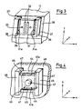
- the concave grating is also designated (14). It has a pin (14a) on its back with which it is held by the manipulator.
- the outer border (14b) of the concave grating (14) sits with a narrow joint (22) in a cylindrical cutout of the mounting plate (23).
- This mounting plate is freely displaceable on the support surface (25) of the chassis (11) and therefore allows the concave grating (14) to be displaced in practically any size in the x and y directions.
- the concave grating (14) can be displaced in the z direction within the cylindrical cutout in the mounting plate (23). It can also be rotated as desired about the z direction and - depending on the width of the gap (22) - can also be rotated more or less about the x and y direction.
- the joint (22) between the concave grid (14) and the mounting plate (23) and the intermediate layer (24) between the mounting plate (23) and the support surface (25) are filled with the solidifying substance. This can be done before the adjustment if it is ensured that the adjustment process is complete before the solidification process begins. Otherwise, the mounting plate (23) with the appropriate amount of the solidifying substance is pushed over the outer border (14b) and pressed onto the support surface (25) when the adjustment of the concave grating (14).
- the volume or layer thickness can be brought to an optimal value by suitable dimensioning of the cylindrical cutout in the mounting plate (23) and by using suitable amounts of the solidifying substance.
- the outer border (14b) of the concave grating a curvature in the z direction, so that the outer border becomes a spherical cutout, the center of which also lies in the center of the concave grating (14) in the z direction.
- relatively large rotations of the concave grating (14) about the y and x axes are possible without the dimensions of the joint being changed.
- FIG 3 the assembly of the diode row is shown, which is glued to the support plate (31) below the plane of the drawing.
- the (not shown) connection pins of the diode line go through two slots (32), so that the first part of the electronics, which is expediently to be arranged as close as possible to the diode line, is arranged above the plane of the drawing.
- two threaded bushes (33) are glued into the support plate (31), into which stud bolts are screwed, which are also used for fastening the support plate (31) to the manipulator during adjustment and fixation.
- the carrier plate (31) has mounting surfaces (31a), on which, after adjustment, thin mounting layers (35) made of the solidifying substance are used to mount mounting blocks (36).
- the mounting cuboids (36) are also placed on the bearing surface (38) of the chassis (11) with thin intermediate layers (37) made of the solidifying substance.
- the carrier plate (31) does not lie on the support surface (38), but has a distance from it, so that it is not only shifted in the x and y directions and rotated about the z direction, but also in the z -Direction can be shifted and rotated around the x-direction. That way is one optimal adjustment possible to different areas of the spectrum generated by the concave grating (14).
- FIG. 4 shows an exemplary embodiment of an optical component (41), e.g. a mirror that can be moved in all three spatial directions and rotated around all three spatial directions.
- the optical component (41) connected to the manipulator via the pin (42) has two mounting surfaces (41a), on which, after adjustment with thin intermediate layers (43) made of the solidifying substance, first mounting cuboids (44) are placed.
- Second assembly cuboids (46) are placed on the end faces of these first assembly cuboids (44) with thin intermediate layers (45) made of the solidifying substance, which at the same time are placed on the support surface (48) with thin intermediate layers (47) made of the solidifying substance.
- FIGS. 5 and 6 show two further exemplary embodiments for the assembly of adjusted optical components.
- the optical component (51) of FIG. 5 can be, for example, a reflection grating, the rear surface of which is used as a mounting surface. It is held at its cylindrical boundary surface by a manipulator.
- a first cuboid mounting plate (53) is placed on the mounting surface with a thin intermediate layer (52) made of the solidifying substance.
- a second cuboid mounting plate (55) is placed, which at the same time has a side surface with a thin intermediate layer (56) made of the solidifying substance on the Base plate (57) is placed.
- the thin surface can be applied to the side surface (58) of the first mounting plate (53)
- a third mounting plate (not shown) is placed on the intermediate layer made of the solidifying substance, which is simultaneously placed on the base plate (57) with a side surface with an intermediate layer made of the solidifying substance.
- the optical component (51) can be moved in all three spatial directions x, y and z during the adjustment and rotated around all three spatial directions.
- a rotation around the z direction is not necessary in many cases, e.g. with plane mirrors.
- FIG. 6 a simpler embodiment is shown in which a side surface of the optical component (61) serves as a mounting surface.
- the cuboid mounting plate (65) is attached to this side surface, which at the same time has a side surface with a thin intermediate layer (66) made of the solidifying substance onto the base plate (67). is put on.
- a further mounting plate (not shown) can be attached to the side surface (68) of the optical component (61) with a thin intermediate layer made of the solidifying substance, which also has a side surface with a thin intermediate layer the solidifying substance is placed on the base plate (67).
- optical components do not have to be connected directly to the mounting blocks or mounting plate by the solidifying substance, but in all exemplary embodiments they can also first be used in sockets or mounted on mounting plates, in which case the sockets or mounting plates with the mounting blocks or Mounting plates are connected by the solidifying substance.
- carrier plates (31), mounting cuboids (36, 44, 46), mounting plate (23, 53, 55, 65) and / or contact surfaces (25, 38, 48, 57, 67) or chassis (11) compacted ceramic the composition of which is selected so that its coefficient of thermal expansion is equal to or approximately equal to that of the glass from which the optical components are made.
- UHU plus (R) can be used as the material for the solidifying substance, which is preferably processed in a layer thickness of approximately 0.1 mm.
Landscapes
- Physics & Mathematics (AREA)
- General Physics & Mathematics (AREA)
- Spectroscopy & Molecular Physics (AREA)
- Optics & Photonics (AREA)
- Chemical & Material Sciences (AREA)
- Organic Chemistry (AREA)
- Mounting And Adjusting Of Optical Elements (AREA)
- Prostheses (AREA)
Applications Claiming Priority (2)
| Application Number | Priority Date | Filing Date | Title |
|---|---|---|---|
| DE3608484A DE3608484C2 (de) | 1986-03-14 | 1986-03-14 | Anordnung zur justierten Montage optischer Bauteile |
| DE3608484 | 1986-03-14 |
Publications (2)
| Publication Number | Publication Date |
|---|---|
| EP0241684A2 true EP0241684A2 (fr) | 1987-10-21 |
| EP0241684A3 EP0241684A3 (fr) | 1990-01-31 |
Family
ID=6296312
Family Applications (1)
| Application Number | Title | Priority Date | Filing Date |
|---|---|---|---|
| EP87102821A Withdrawn EP0241684A3 (fr) | 1986-03-14 | 1987-02-27 | Procédé et arrangement pour l'assemblage ajusté des éléments optiques |
Country Status (4)
| Country | Link |
|---|---|
| US (1) | US4805993A (fr) |
| EP (1) | EP0241684A3 (fr) |
| JP (1) | JPS62220914A (fr) |
| DE (1) | DE3608484C2 (fr) |
Cited By (1)
| Publication number | Priority date | Publication date | Assignee | Title |
|---|---|---|---|---|
| EP0591758A1 (fr) * | 1992-09-26 | 1994-04-13 | Forschungszentrum Karlsruhe GmbH | Appareil d'analyse pour plusieurs composants |
Families Citing this family (7)
| Publication number | Priority date | Publication date | Assignee | Title |
|---|---|---|---|---|
| JPH0580268A (ja) * | 1991-06-28 | 1993-04-02 | Toshiba Corp | 光学装置及びその固定方法 |
| DE19504834C1 (de) | 1995-02-14 | 1996-06-13 | Hewlett Packard Gmbh | Diodenzeilen-Spektralphotometer |
| DE19504835C1 (de) | 1995-02-14 | 1996-03-21 | Hewlett Packard Gmbh | Diodenzeilen-Spektralphotometer |
| JP3228862B2 (ja) * | 1995-11-27 | 2001-11-12 | 松下電器産業株式会社 | 光電圧センサ |
| JPH1090576A (ja) * | 1996-09-17 | 1998-04-10 | Fuji Photo Film Co Ltd | 光学部材の固定構造 |
| US20040047571A1 (en) * | 2002-09-06 | 2004-03-11 | Boord Warren Timothy | Hermetically sealed ferrule |
| US20060082771A1 (en) * | 2004-10-14 | 2006-04-20 | Agilent Technologies, Inc. | Mount of optical components |
Family Cites Families (11)
| Publication number | Priority date | Publication date | Assignee | Title |
|---|---|---|---|---|
| BE593911A (fr) * | 1959-08-17 | |||
| DE1472190A1 (de) * | 1965-07-07 | 1969-01-09 | Rodenstock Optik G | Justierbare Halterung fuer Spiegel u.dgl. |
| US4357072A (en) * | 1978-01-28 | 1982-11-02 | Plessey Handel Und Investments Ag | Sealing optical fibres into packages |
| US4237474A (en) * | 1978-10-18 | 1980-12-02 | Rca Corporation | Electroluminescent diode and optical fiber assembly |
| US4227950A (en) * | 1979-04-05 | 1980-10-14 | Corning Glass Works | Direct casting method for producing low-stress glass/plastic composite lenses |
| JPS5778004A (en) * | 1980-10-31 | 1982-05-15 | Fuji Photo Film Co Ltd | Method for precise positioning |
| DE3138296A1 (de) * | 1981-09-25 | 1983-04-28 | Siemens AG, 1000 Berlin und 8000 München | Verfahren zum positionieren und fixieren von optischen bauelementen relativ zueinander |
| DE3211868A1 (de) * | 1982-03-31 | 1983-05-26 | Fa. Carl Zeiss, 7920 Heidenheim | Chassis fuer optische geraete |
| DE3211867A1 (de) * | 1982-03-31 | 1983-06-01 | Fa. Carl Zeiss, 7920 Heidenheim | Verfahren und vorrichtung zum justieren und montieren von optischen bauteilen in optischen geraeten |
| JPS6043889A (ja) * | 1983-08-22 | 1985-03-08 | Hitachi Ltd | 光ファイバー付レーザーダイオード装置の組立方法 |
| JPS61116306A (ja) * | 1984-10-19 | 1986-06-03 | Fuji Photo Film Co Ltd | 結像レンズの保持装置 |
-
1986
- 1986-03-14 DE DE3608484A patent/DE3608484C2/de not_active Expired - Lifetime
-
1987
- 1987-02-27 EP EP87102821A patent/EP0241684A3/fr not_active Withdrawn
- 1987-03-13 JP JP62056974A patent/JPS62220914A/ja active Pending
- 1987-03-13 US US07/025,718 patent/US4805993A/en not_active Expired - Lifetime
Cited By (1)
| Publication number | Priority date | Publication date | Assignee | Title |
|---|---|---|---|---|
| EP0591758A1 (fr) * | 1992-09-26 | 1994-04-13 | Forschungszentrum Karlsruhe GmbH | Appareil d'analyse pour plusieurs composants |
Also Published As
| Publication number | Publication date |
|---|---|
| EP0241684A3 (fr) | 1990-01-31 |
| JPS62220914A (ja) | 1987-09-29 |
| DE3608484C2 (de) | 2001-07-05 |
| DE3608484A1 (de) | 1987-09-17 |
| US4805993A (en) | 1989-02-21 |
Similar Documents
| Publication | Publication Date | Title |
|---|---|---|
| EP0090218B1 (fr) | Méthode et appareil pour l'adjustage et le montage des éléments optiques à des instruments optiques | |
| DE69320762T2 (de) | Mit hoher Genauigkeit bewegliche Plattform | |
| DE3509131A1 (de) | Verfahren zur justierten montage der optischen bauteile eines optischen geraetes | |
| DE4436176A1 (de) | Sputterquelle mit Targetanordnung und Halterung | |
| EP0463297A1 (fr) | Dispositif comprenant un substrat et un composant et procédé de fabrication | |
| DE4042431C2 (de) | Vorrichtung zur Einstellung der optischen Achsen in einer TV-Kamera | |
| EP1046938A2 (fr) | Dispositif de connection | |
| EP0241684A2 (fr) | Procédé et arrangement pour l'assemblage ajusté des éléments optiques | |
| EP0353436A1 (fr) | Dispositif d'ajustage, notamment pour des outils | |
| DE60303891T2 (de) | Kameraeinheit und Verfahren zu deren Herstellung | |
| DE69230222T2 (de) | Verfahren zur fixierung eines optischen bildsensors in ausrichtung zur bildfläche einer linsenanordnung | |
| DE102018125709A1 (de) | Befestigungssystem eines Head-Up-Displays eines Kraftfahrzeugs, Head-Up-Display für ein Kraftfahrzeug, Montagelehre für ein Head-Up-Display eines Kraftfahrzeugs und Einlehrverfahren für ein Head-Up-Display eines Kraftfahrzeugs | |
| EP1390792B9 (fr) | Systeme de positionnement | |
| EP1006564A1 (fr) | Méthode de fabrication d'un support pour plaquettes semiconductrices et dispositif de support | |
| DE102022211399A1 (de) | Kameramodul und Verfahren zum Aufbau eines Kameramoduls | |
| DE102020134653B3 (de) | Justierbarer Optikhalter für ein optisches Element | |
| EP0068493A1 (fr) | Assemblage de sondes d'essai pour circuits intégrés | |
| EP1329095B1 (fr) | Commande pour microechantillonnage | |
| DE102021107327B3 (de) | Kalottenvorrichtung und Verfahren zum Ausrichten eines Oberelements gegenüber einem Unterelement für eine Positioniervorrichtung und Positioniervorrichtung | |
| EP0374298A1 (fr) | Distributeur de lumière pour un appareil de radiodiagnostic | |
| CH672276A5 (fr) | ||
| DE102007029725A1 (de) | Vorrichtung zur Herstellung von Flüssigkeitsschichten mit vorbestimmter Dicke auf einem Träger | |
| CH670320A5 (fr) | ||
| DD222431B1 (de) | Haltevorrichtung fuer mikroskopobjekttraeger | |
| EP1734743A2 (fr) | Support de circuit imprimé pour un capteur |
Legal Events
| Date | Code | Title | Description |
|---|---|---|---|
| PUAI | Public reference made under article 153(3) epc to a published international application that has entered the european phase |
Free format text: ORIGINAL CODE: 0009012 |
|
| 17P | Request for examination filed |
Effective date: 19870227 |
|
| AK | Designated contracting states |
Kind code of ref document: A2 Designated state(s): CH DE FR GB LI NL |
|
| PUAL | Search report despatched |
Free format text: ORIGINAL CODE: 0009013 |
|
| AK | Designated contracting states |
Kind code of ref document: A3 Designated state(s): CH DE FR GB LI NL |
|
| STAA | Information on the status of an ep patent application or granted ep patent |
Free format text: STATUS: THE APPLICATION IS DEEMED TO BE WITHDRAWN |
|
| 18D | Application deemed to be withdrawn |
Effective date: 19900801 |
|
| RIN1 | Information on inventor provided before grant (corrected) |
Inventor name: BLUMENTRITT, MARTIN Inventor name: SCHNEIDER, HORST Inventor name: GLUECK, FRANZ Inventor name: GERLINGER, HERMANN, DR. |