EP0193331A2 - Verfahren zur Herstellung eines Musters von dotiertem Polysilicium - Google Patents
Verfahren zur Herstellung eines Musters von dotiertem Polysilicium Download PDFInfo
- Publication number
- EP0193331A2 EP0193331A2 EP86301097A EP86301097A EP0193331A2 EP 0193331 A2 EP0193331 A2 EP 0193331A2 EP 86301097 A EP86301097 A EP 86301097A EP 86301097 A EP86301097 A EP 86301097A EP 0193331 A2 EP0193331 A2 EP 0193331A2
- Authority
- EP
- European Patent Office
- Prior art keywords
- circuit
- dopant
- polysilicon
- doped
- doped polysilicon
- Prior art date
- Legal status (The legal status is an assumption and is not a legal conclusion. Google has not performed a legal analysis and makes no representation as to the accuracy of the status listed.)
- Granted
Links
Images
Classifications
-
- H10P14/3802—
-
- H10P14/3411—
-
- H10P34/422—
-
- H10P95/00—
Definitions
- This invention relates to integrated circuits, and in particular to the provision of polysilicon conductors on such circuits.
- Polycrystalline silicon, or polysilicon is frequently used in the fabrication of conductive regions, e.g. gates and interconnection tracks, on integrated circuits. Its use, particularly in high frequency applications, is however limited by the relatively high resistivity of the material. Attempts have been made to overcome this problem by doping the polysilicon typically with phosphorus, arsenic or boron. It is then necessary to anneal the material to diffuse the dopant thereby achieving the desired low resistivity.
- the object of the present invention is to minimise or to overcome this disadvantage.
- a process for forming a doped polysilicon pattern on an integrated circuit including providing the doped pattern on the circuit, and pulse heating the assembly to a temperature at which redistribution of the dopant in the polysilicon is effected whereby the resistivity of the doped polysilicon is reduced.
- a process for forming a doped polysilicon conductive layer on an integrated circuit including providing a doped amorphous silicon layer on said circuit, annealing the circuit at a temperature of 500 to 900°C for a sufficient time to recrystallise the amorphous silicon to form doped polysilicon, and pulse heating the circuit to 1000 to 1110 0 C thereby activating the dopant whereby the resistivity of the polysilicon is reduced.
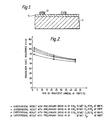
- a semiconductor substrate 11 incorporating a plurality of active devices is provided with an insulating layer 12 of a refractory material, e.g. silica or silicon nitride.
- the insulating layer is in turn coated with a patterned layer 13 of doped polycrystalline silicon.
- the assembly comprises a merged technology circuit in which a number of both CMOS and bipolar devices are provided on a common substrate.
- the polysilicon layer 13 may thus provide an interconnection pattern, the CMOS gates, and bipolar polysilicon emitters.
- the resistivity of the polysilicon 13 is reduced by effecting recitivation of the dopant. This is performed by pulse heating the assembly to a temperature at which reactivation occurs. As this thermal treatment is relatively short there is no significant effect on circuit devices formed in the substrate 11.
- an integrated circuit is provided with a doped polysilicon conductor pattern formed from an amorphous silicon layer.
- a doped polysilicon conductor pattern formed from an amorphous silicon layer.
- Such a layer may be deposited by LPCVD (low pressure chemical vapour deposition), PECVD (plasma enhanced chemical vapour deposition) or reactive sputtering.
- the amorphous silicon is doped, e.g. with phosphorus, arsenic or boron. Doping can be effected chemically during growth or subsequently by ion implantation.
- the assembly is then heated to a temperature of 500 to 1000°C to recrystallise the material to form polysilicon. At the relatively low temperatures employed to effect this recrystallisation substantially no dopant redistribution occurs in the integrated circuit.
- the dopant comprises 0.3 to 3 At % of the amorphous silicon.
- the dopant is fully activated by a short high temperature excursion to e.g. 1000 to 1110°C for 0.5 to 5 seconds in a transient annealing apparatus.
- transient annealing to activate the dopants minimises segregation to grain boundaries and thus provides a high dopant activity and a low resistivity.
- the final resistivity is from 2 to 15 m ohm cm.
- Masking and etching of the silicon layer to define the desired conductor pattern may be performed at a convenient stage in the process. Typically, etching is effected after crystallisation but before dopant activation.
- the silicon layer 13 may be deposited as a doped or undoped material in polycrystalline form, thus obviating the recrystallisation step in the process. Where undoped material is used, doping may be effected by ion implantation.
- in situ phosphorus doped amorphous silicon films containing 0.3 At % of dopant were found to have a resistivity of 25 m ohm cm.
- the films were annealed at 850°C for 50 minutes to recrystallise the silicon and then had a measured resistivity of 20 m ohm cm.
- Pulse annealing of the films for 1 second at 1100°C using incoherent radiation provided a final resistivity of 14 m ohm cm.
- treated films containing 2.5 At % phosphorus had a measured resistivity of 6.2 m ohm cm after annealing for 1 second at 1000°C compared with 30 m ohm cm prior to recrystallisation.
- annealing time and sheet resistance is illustrated in Fig. 2 of the accompanying drawings. Measurements have been made on four silicon films each of 4300A (430nm) thickness. In each case the material was implanted with arsenic at 40 keV with a dose of 1.5E16 cm -2 followed by a preliminary drive in at 900°C. The final sheet resistances observed correspond to resistivities in the range 2.4 to 3.65 m ohm cm.
- transient annealing for dopant activation together with low regrowth temperatures is particularly suited to the low temperature process requirements for advanced CMOS and bipolar circuits. It is not however limited to these particular processes and has general semiconductor application.
Landscapes
- Internal Circuitry In Semiconductor Integrated Circuit Devices (AREA)
- Recrystallisation Techniques (AREA)
- Bipolar Transistors (AREA)
- Semiconductor Integrated Circuits (AREA)
- Amplifiers (AREA)
- Metal-Oxide And Bipolar Metal-Oxide Semiconductor Integrated Circuits (AREA)
- Bipolar Integrated Circuits (AREA)
- Silicon Polymers (AREA)
Priority Applications (1)
| Application Number | Priority Date | Filing Date | Title |
|---|---|---|---|
| AT86301097T ATE61158T1 (de) | 1985-02-23 | 1986-02-18 | Verfahren zur herstellung eines musters von dotiertem polysilicium. |
Applications Claiming Priority (2)
| Application Number | Priority Date | Filing Date | Title |
|---|---|---|---|
| GB858504725A GB8504725D0 (en) | 1985-02-23 | 1985-02-23 | Integrated circuits |
| GB8504725 | 1985-02-23 |
Publications (3)
| Publication Number | Publication Date |
|---|---|
| EP0193331A2 true EP0193331A2 (de) | 1986-09-03 |
| EP0193331A3 EP0193331A3 (en) | 1988-01-27 |
| EP0193331B1 EP0193331B1 (de) | 1991-02-27 |
Family
ID=10574994
Family Applications (1)
| Application Number | Title | Priority Date | Filing Date |
|---|---|---|---|
| EP86301097A Expired - Lifetime EP0193331B1 (de) | 1985-02-23 | 1986-02-18 | Verfahren zur Herstellung eines Musters von dotiertem Polysilicium |
Country Status (5)
| Country | Link |
|---|---|
| EP (1) | EP0193331B1 (de) |
| JP (1) | JPH0693457B2 (de) |
| AT (1) | ATE61158T1 (de) |
| DE (1) | DE3677612D1 (de) |
| GB (2) | GB8504725D0 (de) |
Cited By (2)
| Publication number | Priority date | Publication date | Assignee | Title |
|---|---|---|---|---|
| WO2001093326A1 (en) * | 2000-05-31 | 2001-12-06 | Infineon Technologies North America Corp. | Process for forming doped epitaxial silicon on a silicon substrate |
| US6506321B1 (en) * | 1997-10-24 | 2003-01-14 | Sumitomo Special Metals Co., Ltd. | Silicon based conductive material and process for production thereof |
Families Citing this family (16)
| Publication number | Priority date | Publication date | Assignee | Title |
|---|---|---|---|---|
| GB2188479B (en) * | 1986-03-26 | 1990-05-23 | Stc Plc | Semiconductor devices |
| JPH01145844A (ja) * | 1987-12-01 | 1989-06-07 | Fujitsu Ltd | 半導体装置の製造方法 |
| US5180690A (en) * | 1988-12-14 | 1993-01-19 | Energy Conversion Devices, Inc. | Method of forming a layer of doped crystalline semiconductor alloy material |
| JPH02201917A (ja) * | 1989-01-30 | 1990-08-10 | Nippon Telegr & Teleph Corp <Ntt> | シリコン膜の形成法 |
| JP2850345B2 (ja) * | 1989-02-09 | 1999-01-27 | ソニー株式会社 | マスタスライス方式の半導体集積回路装置 |
| JP2797371B2 (ja) * | 1989-02-10 | 1998-09-17 | ソニー株式会社 | マスタスライス方式の半導体集積回路装置及びその製造方法 |
| US5242507A (en) * | 1989-04-05 | 1993-09-07 | Boston University | Impurity-induced seeding of polycrystalline semiconductors |
| JP2508948B2 (ja) * | 1991-06-21 | 1996-06-19 | 日本電気株式会社 | 半導体装置の製造方法 |
| JPH05343316A (ja) * | 1991-09-30 | 1993-12-24 | Nec Corp | 半導体装置の製造方法 |
| US5403762A (en) * | 1993-06-30 | 1995-04-04 | Semiconductor Energy Laboratory Co., Ltd. | Method of fabricating a TFT |
| US6323071B1 (en) | 1992-12-04 | 2001-11-27 | Semiconductor Energy Laboratory Co., Ltd. | Method for forming a semiconductor device |
| JP2601136B2 (ja) * | 1993-05-07 | 1997-04-16 | 日本電気株式会社 | 半導体装置の製造方法 |
| US6875628B1 (en) * | 1993-05-26 | 2005-04-05 | Semiconductor Energy Laboratory Co., Ltd. | Semiconductor device and fabrication method of the same |
| JP3450376B2 (ja) | 1993-06-12 | 2003-09-22 | 株式会社半導体エネルギー研究所 | 半導体装置の作製方法 |
| US5792700A (en) * | 1996-05-31 | 1998-08-11 | Micron Technology, Inc. | Semiconductor processing method for providing large grain polysilicon films |
| EP0917185B1 (de) * | 1997-11-14 | 2009-01-07 | STMicroelectronics S.r.l. | Verfahren zur Abscheidung von in-situ dotierten Polysilizium-Schichten |
Family Cites Families (9)
| Publication number | Priority date | Publication date | Assignee | Title |
|---|---|---|---|---|
| US4179528A (en) * | 1977-05-18 | 1979-12-18 | Eastman Kodak Company | Method of making silicon device with uniformly thick polysilicon |
| US4214918A (en) * | 1978-10-12 | 1980-07-29 | Stanford University | Method of forming polycrystalline semiconductor interconnections, resistors and contacts by applying radiation beam |
| US4229502A (en) * | 1979-08-10 | 1980-10-21 | Rca Corporation | Low-resistivity polycrystalline silicon film |
| JPS5814567A (ja) * | 1981-07-17 | 1983-01-27 | Nec Corp | 半導体装置及びその製造方法 |
| JPS5837913A (ja) * | 1981-08-28 | 1983-03-05 | Matsushita Electric Ind Co Ltd | 半導体装置の製造方法 |
| GB2106709B (en) * | 1981-09-17 | 1986-11-12 | Itt Ind Ltd | Semiconductor processing |
| GB2130009B (en) * | 1982-11-12 | 1986-04-03 | Rca Corp | Polycrystalline silicon layers for semiconductor devices |
| US4539431A (en) * | 1983-06-06 | 1985-09-03 | Sera Solar Corporation | Pulse anneal method for solar cell |
| GB2143083B (en) * | 1983-07-06 | 1987-11-25 | Standard Telephones Cables Ltd | Semiconductor structures |
-
1985
- 1985-02-23 GB GB858504725A patent/GB8504725D0/en active Pending
-
1986
- 1986-02-18 DE DE8686301097T patent/DE3677612D1/de not_active Expired - Fee Related
- 1986-02-18 EP EP86301097A patent/EP0193331B1/de not_active Expired - Lifetime
- 1986-02-18 AT AT86301097T patent/ATE61158T1/de not_active IP Right Cessation
- 1986-02-20 GB GB08604278A patent/GB2171844B/en not_active Expired
- 1986-02-21 JP JP61038138A patent/JPH0693457B2/ja not_active Expired - Fee Related
Cited By (2)
| Publication number | Priority date | Publication date | Assignee | Title |
|---|---|---|---|---|
| US6506321B1 (en) * | 1997-10-24 | 2003-01-14 | Sumitomo Special Metals Co., Ltd. | Silicon based conductive material and process for production thereof |
| WO2001093326A1 (en) * | 2000-05-31 | 2001-12-06 | Infineon Technologies North America Corp. | Process for forming doped epitaxial silicon on a silicon substrate |
Also Published As
| Publication number | Publication date |
|---|---|
| GB2171844A (en) | 1986-09-03 |
| JPS61229346A (ja) | 1986-10-13 |
| JPH0693457B2 (ja) | 1994-11-16 |
| GB8504725D0 (en) | 1985-03-27 |
| GB2171844B (en) | 1988-12-21 |
| DE3677612D1 (de) | 1991-04-04 |
| ATE61158T1 (de) | 1991-03-15 |
| EP0193331B1 (de) | 1991-02-27 |
| EP0193331A3 (en) | 1988-01-27 |
| GB8604278D0 (en) | 1986-03-26 |
Similar Documents
| Publication | Publication Date | Title |
|---|---|---|
| EP0193331B1 (de) | Verfahren zur Herstellung eines Musters von dotiertem Polysilicium | |
| US4229502A (en) | Low-resistivity polycrystalline silicon film | |
| US4309224A (en) | Method for manufacturing a semiconductor device | |
| KR19990072884A (ko) | 다결정실리콘구조물의제조방법 | |
| EP0111099A1 (de) | Verfahren zum Herstellen komplementärer Metall-Oxid-Halbleiterstrukturen | |
| JPS61501358A (ja) | 中間金属シリサイド層を有する改良型集積回路構造およびその製作方法 | |
| JPH0777259B2 (ja) | 所望の温度係数を持った多結晶シリコン抵抗の製造方法 | |
| EP0051500B1 (de) | Halbleiterbauelement | |
| US4354307A (en) | Method for mass producing miniature field effect transistors in high density LSI/VLSI chips | |
| CA1210525A (en) | Method of manufacturing a high resistance layer having a low temperature coefficient of resistance and semi-conductor device having such high resistance layer | |
| US5837592A (en) | Method for stabilizing polysilicon resistors | |
| US4502894A (en) | Method of fabricating polycrystalline silicon resistors in integrated circuit structures using outdiffusion | |
| EP0085918A2 (de) | Verfahren zur Herstellung von Metallsiliziden | |
| US4707909A (en) | Manufacture of trimmable high value polycrystalline silicon resistors | |
| EP0073075A2 (de) | Halbleiteranordnung mit polykristallinem Silizium und Verfahren zu deren Herstellung | |
| US6191018B1 (en) | Method for selective resistivity adjustment of polycide lines for enhanced design flexibility and improved space utilization in sub-micron integrated circuits | |
| KR20010007504A (ko) | 집적된 저항 콘택 | |
| US4851359A (en) | Method of producing an electrical resistor by implanting a semiconductor material with rare gas | |
| US5712196A (en) | Method for producing a low resistivity polycide | |
| US5554549A (en) | Salicide process for FETs | |
| US4416055A (en) | Method of fabricating a monolithic integrated circuit structure | |
| JP2798043B2 (ja) | 半導体装置の製造方法 | |
| Kwong | Rapid thermal annealing of co-sputtered tantalum silicide films | |
| EP0255968A2 (de) | Polykristalliner Siliziumfilm mit hohem Schichtwiderstand für anwachsende Durchbruchsspannung | |
| EP1017092A1 (de) | Herstellung eines in einer integrierten Schaltung verwendeten Widerstands |
Legal Events
| Date | Code | Title | Description |
|---|---|---|---|
| PUAI | Public reference made under article 153(3) epc to a published international application that has entered the european phase |
Free format text: ORIGINAL CODE: 0009012 |
|
| AK | Designated contracting states |
Kind code of ref document: A2 Designated state(s): AT BE CH DE FR IT LI LU NL SE |
|
| RAP1 | Party data changed (applicant data changed or rights of an application transferred) |
Owner name: STC PLC |
|
| PUAL | Search report despatched |
Free format text: ORIGINAL CODE: 0009013 |
|
| AK | Designated contracting states |
Kind code of ref document: A3 Designated state(s): AT BE CH DE FR IT LI LU NL SE |
|
| 17P | Request for examination filed |
Effective date: 19880218 |
|
| 17Q | First examination report despatched |
Effective date: 19891208 |
|
| ITF | It: translation for a ep patent filed | ||
| GRAA | (expected) grant |
Free format text: ORIGINAL CODE: 0009210 |
|
| AK | Designated contracting states |
Kind code of ref document: B1 Designated state(s): AT BE CH DE FR IT LI LU NL SE |
|
| PG25 | Lapsed in a contracting state [announced via postgrant information from national office to epo] |
Ref country code: SE Effective date: 19910227 Ref country code: LI Effective date: 19910227 Ref country code: CH Effective date: 19910227 Ref country code: BE Effective date: 19910227 Ref country code: AT Effective date: 19910227 |
|
| REF | Corresponds to: |
Ref document number: 61158 Country of ref document: AT Date of ref document: 19910315 Kind code of ref document: T |
|
| ET | Fr: translation filed | ||
| REF | Corresponds to: |
Ref document number: 3677612 Country of ref document: DE Date of ref document: 19910404 |
|
| REG | Reference to a national code |
Ref country code: CH Ref legal event code: PL |
|
| PLBE | No opposition filed within time limit |
Free format text: ORIGINAL CODE: 0009261 |
|
| STAA | Information on the status of an ep patent application or granted ep patent |
Free format text: STATUS: NO OPPOSITION FILED WITHIN TIME LIMIT |
|
| 26N | No opposition filed | ||
| PG25 | Lapsed in a contracting state [announced via postgrant information from national office to epo] |
Ref country code: LU Free format text: LAPSE BECAUSE OF NON-PAYMENT OF DUE FEES Effective date: 19920229 |
|
| ITPR | It: changes in ownership of a european patent |
Owner name: CAMBIO RAGIONE SOCIALE;NORTHERN TELECOM EUROPE LIM |
|
| NLT1 | Nl: modifications of names registered in virtue of documents presented to the patent office pursuant to art. 16 a, paragraph 1 |
Owner name: STC LIMITED TE LONDEN, GROOT-BRITTANNIE. |
|
| NLT1 | Nl: modifications of names registered in virtue of documents presented to the patent office pursuant to art. 16 a, paragraph 1 |
Owner name: NORTHERN TELECOM EUROPE LIMITED TE LONDON, GROOT-B |
|
| REG | Reference to a national code |
Ref country code: FR Ref legal event code: TP |
|
| NLT1 | Nl: modifications of names registered in virtue of documents presented to the patent office pursuant to art. 16 a, paragraph 1 |
Owner name: STC LIMITED TE MAIDENHEAD, GROOT-BRITTANNIE. |
|
| NLS | Nl: assignments of ep-patents |
Owner name: NORTHERN TELECOM LIMITED IN MONTREAL, CANADA |
|
| NLT1 | Nl: modifications of names registered in virtue of documents presented to the patent office pursuant to art. 16 a, paragraph 1 |
Owner name: NORTEL NETWORKS LIMITED;NORTHERN TELECOM LIMITED |
|
| PGFP | Annual fee paid to national office [announced via postgrant information from national office to epo] |
Ref country code: NL Payment date: 20040127 Year of fee payment: 19 |
|
| PGFP | Annual fee paid to national office [announced via postgrant information from national office to epo] |
Ref country code: FR Payment date: 20040202 Year of fee payment: 19 |
|
| PGFP | Annual fee paid to national office [announced via postgrant information from national office to epo] |
Ref country code: DE Payment date: 20040227 Year of fee payment: 19 |
|
| REG | Reference to a national code |
Ref country code: FR Ref legal event code: CD |
|
| PG25 | Lapsed in a contracting state [announced via postgrant information from national office to epo] |
Ref country code: IT Free format text: LAPSE BECAUSE OF NON-PAYMENT OF DUE FEES;WARNING: LAPSES OF ITALIAN PATENTS WITH EFFECTIVE DATE BEFORE 2007 MAY HAVE OCCURRED AT ANY TIME BEFORE 2007. THE CORRECT EFFECTIVE DATE MAY BE DIFFERENT FROM THE ONE RECORDED. Effective date: 20050218 |
|
| PG25 | Lapsed in a contracting state [announced via postgrant information from national office to epo] |
Ref country code: NL Free format text: LAPSE BECAUSE OF NON-PAYMENT OF DUE FEES Effective date: 20050901 Ref country code: DE Free format text: LAPSE BECAUSE OF NON-PAYMENT OF DUE FEES Effective date: 20050901 |
|
| PG25 | Lapsed in a contracting state [announced via postgrant information from national office to epo] |
Ref country code: FR Free format text: LAPSE BECAUSE OF NON-PAYMENT OF DUE FEES Effective date: 20051031 |
|
| NLV4 | Nl: lapsed or anulled due to non-payment of the annual fee |
Effective date: 20050901 |
|
| REG | Reference to a national code |
Ref country code: FR Ref legal event code: ST Effective date: 20051031 |