EP0186459A2 - Mémoire à semi-conducteur avec générateur de formes de test - Google Patents
Mémoire à semi-conducteur avec générateur de formes de test Download PDFInfo
- Publication number
- EP0186459A2 EP0186459A2 EP85309305A EP85309305A EP0186459A2 EP 0186459 A2 EP0186459 A2 EP 0186459A2 EP 85309305 A EP85309305 A EP 85309305A EP 85309305 A EP85309305 A EP 85309305A EP 0186459 A2 EP0186459 A2 EP 0186459A2
- Authority
- EP
- European Patent Office
- Prior art keywords
- memory cell
- test pattern
- cell array
- signal
- address signals
- Prior art date
- Legal status (The legal status is an assumption and is not a legal conclusion. Google has not performed a legal analysis and makes no representation as to the accuracy of the status listed.)
- Granted
Links
Images


Classifications
-
- H—ELECTRICITY
- H01—ELECTRIC ELEMENTS
- H01L—SEMICONDUCTOR DEVICES NOT COVERED BY CLASS H10
- H01L27/00—Devices consisting of a plurality of semiconductor or other solid-state components formed in or on a common substrate
- H01L27/02—Devices consisting of a plurality of semiconductor or other solid-state components formed in or on a common substrate including semiconductor components specially adapted for rectifying, oscillating, amplifying or switching and having at least one potential-jump barrier or surface barrier; including integrated passive circuit elements with at least one potential-jump barrier or surface barrier
-
- G—PHYSICS
- G11—INFORMATION STORAGE
- G11C—STATIC STORES
- G11C29/00—Checking stores for correct operation ; Subsequent repair; Testing stores during standby or offline operation
- G11C29/04—Detection or location of defective memory elements, e.g. cell constructio details, timing of test signals
- G11C29/08—Functional testing, e.g. testing during refresh, power-on self testing [POST] or distributed testing
- G11C29/12—Built-in arrangements for testing, e.g. built-in self testing [BIST] or interconnection details
- G11C29/46—Test trigger logic
-
- G—PHYSICS
- G11—INFORMATION STORAGE
- G11C—STATIC STORES
- G11C29/00—Checking stores for correct operation ; Subsequent repair; Testing stores during standby or offline operation
Definitions
- the present invention relates to a semiconductor device incorporating a memory cell array, for example, a random-access memory (RAM).
- a memory cell array for example, a random-access memory (RAM).
- a memory cell array for example, RAM
- various kinds of logic circuits are provided in addition to the memory cell array for transmitting or receiving signals to or from the array.
- Such logic circuits include, for example, counter circuits and arithmetic logic units (ALU). Address signals for the memory cell array are supplied from the output side of the counter circuits, and data which has been calculated in the ALU's is supplied from the output side of ALU's to the array and written into the predetermined address. Also, predetermined data read from the memory cell array is supplied to the input side of the ALU's in order, for example, to carry out predetermined calculation in the ALU's again.
- ALU arithmetic logic units
- test data to be written into the memory cell array was designated from the outside. Therefore, there was the problem that it was necessary to use a large amount of test data, resulting in poor efficiency for the testing.
- test pattern constituting the test data to be written into each memory cell becomes large, especially when the capacity of the memory cell array is large. As a result, the writing of the test data for the memory cell array would still be troublesome.
- a semiconductor device comprising: a memory cell array; a test pattern generating circuit; and means for receiving a control signal from the outside; the test pattern generating circuit being operable for generating a test pattern and transmitting the test pattern to the memory cell array when receiving a least significant bit signal of address signals supplied to the memory cell array and the control signal.
- An embodiment of the present invention may enable automatic generation of a pattern of test data just by supplying address signals for the memory cell array (for example, RAM), without the necessity of supplying test data from the outside.
- the memory cell array for example, RAM
- test data to be written into adjacent memory cells consists of alternate "1"'s and "0"'s.
- This test pattern recently known is simple, but desirable in that it can detect exactly defective parts of the memory cell array.
- An embodiment of the present invention may provide a semiconductor device incorporating a test pattern generating circuit able to test the internal state of the memory cell array before shipment of the semiconductor device.
- the address signals are row address signals for the memory cell array, for example, the least significant bit signal of the row address signals changes alternately between "0" and "1" every time each adjacent row address (namely, each of even row address and odd row address) is input in turn.
- the desired test pattern the checkerboard pattern, for example
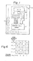
- Figure 1 is a schematic block diagram illustrating the overall constitution of a semiconductor device incorporating a memory cell array.
- a memory cell array 1 for example, RAM
- a logic circuit area 10 on a chip 12 which logic circuits transmit or receive signals (for example, address signals A 0 to An and data signals D 0 to D m ) to or from the memory cell array 1.
- a counter circuit 101 and an arithmetic logic unit (ALU) 102 for example, in the above logic circuit area 10.
- the address signals A 0 to A for the memory cell array 1 are supplied from the output side of the counter circuit 101.
- Data D 0 to D which has been calculated in the ALU 102 is m supplied from the output side of ALU 102 to the memory cell array 1 and written into predetermined memory cells of the memory cell array 1.
- Predetermined data read from the memory cell array 1 is also supplied to the input side of the ALU 102 in order to carry out a predetermined calculation in the ALU 102 again, for example.
- Input and output circuits 11 are provided around the chip 12. Signals are transmitted between the above semiconductor device and the external circuit through the I/O circuits 11.
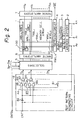
- Figure 2 illustrates the constitution of a test pattern generating circuit and connections between the test pattern generating circuit and the memory cell array in a semiconductor device according to one embodiment of the present invention.
- a memory cell array (RAM) 1. Only row address signals A O to An are supplied as the address signals, i.e., no column address signals are used.
- the row address signals A 0 to An are input to corresponding address buffers 2.
- the address buffers 2 output the internal row address signals A 0 , A 0 (the inverted signal of the signal A O ) to An , An (the inverted signal of the signal An), respectively, and supply these internal row address signals to the corre- spondin g row decoders 3.
- the row decoders 3 select the predetermined word line.
- both write word linesand read word lines are used as word lines.
- a switching circuit 4 supplies the selecting signal to the selected write word line (for example, WWL 0 ).
- the switching circuit 4 supplies the selecting signal to the selected read word line (for example, RWL O ).
- selectors 5 and write amplifiers 6 are connected to the data input side of the memory cell array 1.
- Sense amplifiers 7 are connected to the data output side of the memory cell array 1.
- control signal CNT2 supplied to the selector 5 becomes low level, for example, the usual data D 0 to D m supplied from the logic circuit area 10 is input through the selectors 5, the write amplifiers 6, and the above write bit lines to the memory cells connected to the selected word line in the memory cell array 1.
- the output data X 0 to X m which is read from the memory cells connected to the selected word line in the memory cell array 1 is output through the read bit lines RBL 0 , RBL 1 , and the like, and the sense amplifiers 7.
- test pattern generating circuit 8 which generates test data to be written into the memory cell array 1 to test the array 1.
- AND gates 83, 84, 85, 86, and the like there are provided AND gates 83, 84, 85, 86, and the like.
- the least significant bit signal A 0 of the row address signals A 0 to An and the inverted signal A 0 produced by inverting the signal A 0 through an inverter 81 are input to AND gates 83 and 84, respectively.
- the above signals A 0 and A 0 are input to the following AND gates 85 and 86, respectively.
- the above signals A 0 and A 0 are input to the further following AND gates in the same manner.
- a control signal CNT1 is input from the outside to the AND gates 83 and 85, through an inverter 82, and to the AND gates 84 and 86 directly. Similarly, the above control signal CNT1 is input to the further following AND gates in the same manner.
- the output signals of a pair of AND gates 83 and 84 are input to an OR gate 87, from where the test data T 0 is output. Also, the output signals of a pair of AND gates 85 and 86 are input to an OR gate 88, from where the test data T 1 is output. Similarly, the output signals of each pair of AND gates are input to the corresponding OR gate, from where the test data T 0 to T m is output.
- the least significant bit signal A 0 of the row address signals supplied to the test pattern generating circuit 8 is also low level.
- the low level signal A 0 is input to each of AND gates 83, 86 -----, and the inverted high level signal A 0 is input through the inverter 81 to each of AND gates 84, 85 -----.
- control signal CNT1 supplied to the test pattern generating circuit 8 is set to low level
- the low level control signal is input directly to each of AND gates 84, 86 -----
- the inverted high level signal produced by inverting the control signal CNT1 through the inverter 82 is input to each of AND gates 83, 85 ------.
- test data T 0 is output as the low level signal (namely, "0").
- the output signal of the following AND gate 85 becomes high level
- the output signal of the OR gate 88 also becomes high level (although the output level of the AND gate 86 is low).
- the test data T 1 is output as the high level signal (namely, "1").
- the test data T 0 to T m of the predetermined level is output from the test pattern generating circuit 8.
- each of the test data T 0 to T m which alternately changes between "0" and "1", as shown in the first row of the pattern shown in Fig. 4A, is written into each memory cell (for example, 1-00) connected to the selected write word line WWL O in the memory cell array 1.
- each of the test data T 0 to T m which alternately changes between "1" and "0", as shown in the second row of the pattern shown in Fig. 4A, is written into each memory cell connected to the selected write word line WWL 1 in the memory cell array 1, through a similar operation as above-mentioned,/
- each of the test data which alternately changes between "0" and "1" as shown in Fig. 4A (namely, each of the test data constituting the above-mentioned checkerboard pattern) is written into each memory cell in the memory cell array 1.
- the active level of the control signal CTN1 is set to the low level, if the active level of the control signal CNT1 is set to the high level, each of the test data constituting another checkerboard pattern as shown in Fig. 4B is written into each memory cell in the memory cell array 1.
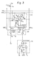
- Figure 3 is a circuit diagram of an example of a memory cell (for example, 1-00) in the above memory cell array 1 and a selector 50, a write amplifier 60, and a sense amplifier 70 connected to the above memory cell.
- a memory cell for example, 1-00
- an inverter 501 As shown in Fig. 3, there are provided an inverter 501, AND gates 502 and 503, and an OR gate 504 in a selector 50.
- the control signal CNT2 becomes high level
- the test data T 0 supplied from the test pattern generating circuit 8 is input to the write amplifier 60 through the gates 502 and 504.
- the control signal CNT2 becomes low level
- the usual data D supplied from the logic circuit area is input to the write amplifier 60 through the gates 503 and 504.
- the write amplifier 60 there are provided an amplifier 601 and an inverter 602.
- the write amplifier 60 is connected to the memory cell 1-00 through the write bit lines WBL O and WBL 0 .
- the memory cell 1-00 there are provided a plurality of transistors Q 1 to Q 8 (among these, transistors Q 1 and Q 2 are P-channel type transistors, and transistors Q 3 to Q 8 are N-channel type transistors).
- the memory cell 1-00 is connected to the write bit lines WBL O and WBL 0 , the read bit line RBL 0 , the write word line WWL 0 , and the read word line RWL 0 .
- a P-channel type transistor Q 9 is connected between the power source V DD and the read bit line RHL 0 , and a clock signal CLK is supplied to the gate of the transistor Q 9 .
- the voltage level of the selected word line WWL 0 becomes high.
- the voltage level of the write bit line WBL 0 supplied through the amplifier 601 becomes high, and, contrary to this, the voltage level of the write bit line WBL O supplied through the amplifier 601 and the inverter 602 becomes low.
- the transistor Q 5 turns on, and the voltage level of the connection point A between the transistors Q 2 and Q 4 becomes high.
- the data "1" is written into the memory cell 1-00.
- the transistor Q 6 also turns on, and the voltage level of the connection point B between the transistors Q 1 and Q 3 becomes low.
- the above-mentioned high level voltage at the connection point A is latched.
- the clock signal CLK becomes low level, and, thus, the memory cell 1-00 is charged up through the P-channel type transistor Q 9 and the read bit line RBL 0 by the power source V DD .
- the transistor Q 8 turns off (because the gate level of the transistor Q is low level).
- the high level data X 0 produced by the above-mentioned charging up is output through the transistor Q 7 , the read bit line RBL 0 , and the sense amplifier 70 in which an amplifier 701 is provided.
- the transistor Q 8 turns on (because the gate level of the transistor Q 8 becomes high).
- the level of the read bit line RBL 0 becomes low (namely, the level of V ) by the discharging through the transistor Q 8 , and the low level data X 0 is output through the sense amplifier 70.
- Figure 5 illustrates the constitution of the test pattern generating circuit and the connections between the test pattern generating circuit and the memory cell array in a semiconductor device according to another embodiment of the present invention.
- FIG. 5 there is shown the memory cell array in this case (RAM) 1' to which/both row address signals and column address signals are supplied as address signals.
- address buffers 2' As shown in Fig. 5, there are provided address buffers 2', row decoders 3', column decoders 4', selectors 5', write amplifiers 6', column selectors 7', and sense amplifiers 8'.
- the memory cell array 1' is physically constituted in the size of four row addresses and four column addresses, as shown in Fig. 6.
- the address signals A 0 to A 2 are input to the corresponding address buffers 2'.
- the address buffers 2' output the internal column address signals A 0 and A O and the internal row address signals A 1 , A 1 , A 2 , and A 2 and supply these internal address signals A 0 to A O and A 1 to A 2 to each of the column decoders 4' and the row decoders 3'.
- the row decoders 3' select the predetermined row address according to the level of the internal row address signals A 1 to A 2 . Also the column decoders 4' select the predetermined column address according to the level of the internal column address signals A 0 and A 0 .
- selectors 5' and the write amplifiers 6' are connected to the data input side of the column selectors 7'.
- the sense amplifiers 8' are connected to the data output side of the column selectors 7'.
- a control signal CNT2 supplied from the outside to the selectors 5' becomes high level, for example, test data of two bits TO and T 1 supplied from the test pattern generating circuit 9 are input through the selectors 5', the write amplifiers 6', and the column selectors 7' to predetermined memory cells in the memory cell array 1'.
- the control signal CNT2 becomes low level, for example, the usual data of two bits D 0 and D 1 supplied from the logic circuit area 10 is input through the selectors 5', the write amplifiers 6', and the column selectors 7' to the predetermined memory cells in the memory cell array 1'.
- the data X 0 and X 1 is output from the predetermined memory cells through the column selectors 7' and the sense amplifiers 8'.
- the column selectors 7' select two column addresses as the addresses to or from which the above data of two bits are input or output, according to the output level of the column decoders 4'.
- test pattern generating circuit 9 which generates the test data to be written into the memory cell array I' in order to test the memory cell array 1'.
- test pattern generating circuit 9 there is provided an exclusive NOR gate 91 to which both of the least significant bit signal A l of the row address signals and the least significant bit signal A 0 of the column address signals are supplied.
- exclusive NOR gate 91 to which both of the least significant bit signal A l of the row address signals and the least significant bit signal A 0 of the column address signals are supplied.
- the above signal A 0 is also the least significant bit signal of the column address signals.
- the output signal of the exclusive NOR gate 91 becomes high level when both levels of the above supplied signals coincide (namely, both high or both low), and becomes low level when the levels of the above supplied signals do not coincide.
- the output signal of the exclusive NOR gate 91 is input to each of the AND gates 94 and 96 directly and is input to each of the AND gates 95 and 97 through an inverter 92. Further, a control signal CNT1 is input from the outside to each of the AND gates 94 and 96 directly and is input to each of the AND gates 95 and 97 through an inverter 93.
- the output signals of a pair of AND gates 94 and 95 are input to an OR gate 98, from where the test data TO is output.
- the output signals of a pair of AND gates 95 and 97 are input to an OR gate 99, from where the test data T 1 is output. Then, the test data T 0 and T 1 is input to the above-mentioned selectors 5'.
- control signal CNT1 is supplied to the AND gates 94 and 96 directly, and the low level signal produced by inverting that control signal CNT1 through the inverter 93 is supplied to the AND gates 95 and 97.
- each output level of the AND gates 94 and 96 becomes high, and, thus, each output level of OR gates 98 and 99 (namely, each level of the test data T 0 and T 1 ) becomes high.
- the high level test data "1" is written into the predetermined two memory cells arranged at the intersection of the row address selected when the row address signals A 1 and A 2 are both low level (namely, the top row address in the pattern shown in Fig. 6) and each of two column addresses selected when the column address signal A 0 is low level (namely, the first and third column addresses from the left side in the pattern shown in Fig. 6).
- the low level test data "0" is written into the predetermined two memory cells arranged at the intersection of the row address selected when the row address signals A 1 and A 2 are low level and high level respectively (namely, the third row address from the top side in the pattern shown in Fig. 6) and each of two column addresses selected when the column address signal A 0 is high level (namely, the second and fourth column addresses from the left side in the pattern shown in Fig. 6).
- each test data constituting the checkerboard pattern as shown in Fig. 6 is written into each memory cell in the memory cell array 1'.
- test data for example, a checkerboard pattern
- transmit the test pattern to the memory cell array just by supplying address signals for the memory cell array, without the necessity of supplying test data from the outside.
Applications Claiming Priority (2)
| Application Number | Priority Date | Filing Date | Title |
|---|---|---|---|
| JP267460/84 | 1984-12-20 | ||
| JP59267460A JPS61145799A (ja) | 1984-12-20 | 1984-12-20 | メモリを内蔵した半導体集積回路 |
Publications (3)
| Publication Number | Publication Date |
|---|---|
| EP0186459A2 true EP0186459A2 (fr) | 1986-07-02 |
| EP0186459A3 EP0186459A3 (en) | 1988-06-08 |
| EP0186459B1 EP0186459B1 (fr) | 1992-07-22 |
Family
ID=17445145
Family Applications (1)
| Application Number | Title | Priority Date | Filing Date |
|---|---|---|---|
| EP85309305A Expired - Lifetime EP0186459B1 (fr) | 1984-12-20 | 1985-12-20 | Mémoire à semi-conducteur avec générateur de formes de test |
Country Status (5)
| Country | Link |
|---|---|
| US (1) | US4701919A (fr) |
| EP (1) | EP0186459B1 (fr) |
| JP (1) | JPS61145799A (fr) |
| KR (1) | KR900008660B1 (fr) |
| DE (1) | DE3586397T2 (fr) |
Cited By (3)
| Publication number | Priority date | Publication date | Assignee | Title |
|---|---|---|---|---|
| EP0263470A2 (fr) * | 1986-10-08 | 1988-04-13 | Siemens Aktiengesellschaft | Procédé et agencements de test de modules de mémoire à mégabits à l'aide de configurations de test arbitraires dans le mode test multibits |
| WO1989002122A1 (fr) * | 1987-08-26 | 1989-03-09 | Siemens Aktiengesellschaft | Agencement et procede de depistage et de localisation de circuits defectueux dans des composants de memorisation |
| DE3906494A1 (de) * | 1988-12-15 | 1990-06-21 | Samsung Electronics Co Ltd | Fehlerbiterzeugungsschaltung zur verwendung in einer nicht-fluechtigen halbleiterspeichervorrichtung |
Families Citing this family (20)
| Publication number | Priority date | Publication date | Assignee | Title |
|---|---|---|---|---|
| JPS61292755A (ja) * | 1985-06-20 | 1986-12-23 | Fujitsu Ltd | 半導体集積回路 |
| JPS6221357A (ja) * | 1985-07-22 | 1987-01-29 | Toshiba Corp | メモリシステム |
| JPS62140299A (ja) * | 1985-12-13 | 1987-06-23 | Advantest Corp | パタ−ン発生装置 |
| JPS62195572A (ja) * | 1986-02-21 | 1987-08-28 | Mitsubishi Electric Corp | 半導体テスト装置 |
| DE3773773D1 (de) * | 1986-06-25 | 1991-11-21 | Nec Corp | Pruefschaltung fuer eine speichereinrichtung mit willkuerlichem zugriff. |
| US4872168A (en) * | 1986-10-02 | 1989-10-03 | American Telephone And Telegraph Company, At&T Bell Laboratories | Integrated circuit with memory self-test |
| JPH0812226B2 (ja) * | 1987-01-14 | 1996-02-07 | 三菱電機株式会社 | 半導体装置 |
| US4801869A (en) * | 1987-04-27 | 1989-01-31 | International Business Machines Corporation | Semiconductor defect monitor for diagnosing processing-induced defects |
| JP2779538B2 (ja) * | 1989-04-13 | 1998-07-23 | 三菱電機株式会社 | 半導体集積回路メモリのためのテスト信号発生器およびテスト方法 |
| US5101409A (en) * | 1989-10-06 | 1992-03-31 | International Business Machines Corporation | Checkboard memory self-test |
| US5073891A (en) * | 1990-02-14 | 1991-12-17 | Intel Corporation | Method and apparatus for testing memory |
| JP2882426B2 (ja) * | 1991-03-29 | 1999-04-12 | 株式会社アドバンテスト | アドレス発生装置 |
| BE1004959A3 (nl) * | 1991-06-28 | 1993-03-02 | Bell Telephone Mfg | Werkwijze en inrichtingen voor het testen van atm-verbindingen. |
| JPH05274895A (ja) * | 1992-03-26 | 1993-10-22 | Nec Ic Microcomput Syst Ltd | 半導体記憶装置 |
| US5490115A (en) * | 1994-07-29 | 1996-02-06 | Cypress Semiconductor Corp. | Method and apparatus for writing to memory cells in a minimum number of cycles during a memory test operation |
| TW338106B (en) * | 1996-03-29 | 1998-08-11 | Adoban Test Kk | Semiconductor memory testing apparatus |
| US6078637A (en) | 1998-06-29 | 2000-06-20 | Cypress Semiconductor Corp. | Address counter test mode for memory device |
| JP2000182398A (ja) * | 1998-12-15 | 2000-06-30 | Nec Corp | 半導体装置及び半導体装置の試験方法 |
| US6728910B1 (en) * | 2000-09-20 | 2004-04-27 | Lsi Logic Corporation | Memory testing for built-in self-repair system |
| TW559970B (en) * | 2001-04-05 | 2003-11-01 | Kawasaki Microelectronics Inc | Test circuit, semiconductor product wafer having the test circuit, and method of monitoring manufacturing process using the test circuit |
Citations (1)
| Publication number | Priority date | Publication date | Assignee | Title |
|---|---|---|---|---|
| JPS573299A (en) * | 1980-06-06 | 1982-01-08 | Nec Corp | Memory integrated circuit |
Family Cites Families (3)
| Publication number | Priority date | Publication date | Assignee | Title |
|---|---|---|---|---|
| US3924181A (en) * | 1973-10-16 | 1975-12-02 | Hughes Aircraft Co | Test circuitry employing a cyclic code generator |
| US4541090A (en) * | 1981-06-09 | 1985-09-10 | Matsushita Electric Industrial Co., Ltd. | Semiconductor memory device |
| US4519078A (en) * | 1982-09-29 | 1985-05-21 | Storage Technology Corporation | LSI self-test method |
-
1984
- 1984-12-20 JP JP59267460A patent/JPS61145799A/ja active Granted
-
1985
- 1985-12-17 KR KR1019850009485A patent/KR900008660B1/ko not_active IP Right Cessation
- 1985-12-18 US US06/810,143 patent/US4701919A/en not_active Expired - Lifetime
- 1985-12-20 DE DE8585309305T patent/DE3586397T2/de not_active Expired - Fee Related
- 1985-12-20 EP EP85309305A patent/EP0186459B1/fr not_active Expired - Lifetime
Patent Citations (1)
| Publication number | Priority date | Publication date | Assignee | Title |
|---|---|---|---|---|
| JPS573299A (en) * | 1980-06-06 | 1982-01-08 | Nec Corp | Memory integrated circuit |
Non-Patent Citations (1)
| Title |
|---|
| PATENT ABSTRACTS OF JAPAN, vol. 6, no. 62 (P-111)[940], 21st April 1982; & JP 57003299 A (NIPPON DENKI K.K.) 08-01-1982 * |
Cited By (5)
| Publication number | Priority date | Publication date | Assignee | Title |
|---|---|---|---|---|
| EP0263470A2 (fr) * | 1986-10-08 | 1988-04-13 | Siemens Aktiengesellschaft | Procédé et agencements de test de modules de mémoire à mégabits à l'aide de configurations de test arbitraires dans le mode test multibits |
| EP0263470A3 (en) * | 1986-10-08 | 1989-11-15 | Siemens Aktiengesellschaft | Method and arrangement for testing megabit memory modules with arbitrary test patterns in a multiple bit test mode |
| WO1989002122A1 (fr) * | 1987-08-26 | 1989-03-09 | Siemens Aktiengesellschaft | Agencement et procede de depistage et de localisation de circuits defectueux dans des composants de memorisation |
| US5123016A (en) * | 1987-08-26 | 1992-06-16 | Siemens Aktiengesellschaft | Arrangement and method for identifying and localizing faulty circuits of a memory module |
| DE3906494A1 (de) * | 1988-12-15 | 1990-06-21 | Samsung Electronics Co Ltd | Fehlerbiterzeugungsschaltung zur verwendung in einer nicht-fluechtigen halbleiterspeichervorrichtung |
Also Published As
| Publication number | Publication date |
|---|---|
| KR860005446A (ko) | 1986-07-23 |
| JPH0378720B2 (fr) | 1991-12-16 |
| KR900008660B1 (ko) | 1990-11-26 |
| US4701919A (en) | 1987-10-20 |
| EP0186459A3 (en) | 1988-06-08 |
| DE3586397T2 (de) | 1993-03-18 |
| DE3586397D1 (de) | 1992-08-27 |
| EP0186459B1 (fr) | 1992-07-22 |
| JPS61145799A (ja) | 1986-07-03 |
Similar Documents
| Publication | Publication Date | Title |
|---|---|---|
| US4701919A (en) | Semiconductor device incorporating memory test pattern generating circuit | |
| US6519192B2 (en) | Semiconductor memory device having a large band width and allowing efficient execution of redundant repair | |
| US6657886B1 (en) | Split local and continuous bitline for fast domino read SRAM | |
| US7035161B2 (en) | Semiconductor integrated circuit | |
| US4972373A (en) | Precharge system in a SRAM | |
| US4758990A (en) | Resetting arrangement for a semiconductor integrated circuit device having semiconductor memory | |
| US4951259A (en) | Semiconductor memory device with first and second word line drivers | |
| EP0530714A2 (fr) | Dispositif de circuit intégré à semi-conducteurs permettant la modification de spécification de produit et méthode d'essai éliminatoire de chip y afférant | |
| EP0655744B1 (fr) | Dispositif de mémoire multibit à semi-conducteurs | |
| US6353570B2 (en) | Row redundancy circuit using a fuse box independent of banks | |
| US4658379A (en) | Semiconductor memory device with a laser programmable redundancy circuit | |
| JPH03203100A (ja) | 半導体メモリ装置の並列テスト方法及び半導体メモリ装置 | |
| EP0443775B1 (fr) | Circuit de signature pour un dispositif de mémoire non-volatile | |
| EP0415408B1 (fr) | Dispositif de mémoire à semi-conducteurs du type MOS | |
| US4630240A (en) | Dynamic memory with intermediate column derode | |
| EP0172112B1 (fr) | Dispositif de mémoire semi-conductrice | |
| US4638461A (en) | Semiconductor memory device | |
| US4644500A (en) | Semiconductor memory device with a controlled precharging arrangement | |
| EP0329182B1 (fr) | Circuit de tampon décodeur incorporé dans un équipement de mémoire à semi-conducteur | |
| US4903239A (en) | Semiconductor memory having a parallel input/output circuit | |
| US20030043648A1 (en) | Semiconductor memory device capable of testing data line redundancy replacement circuit | |
| US6735147B2 (en) | Semiconductor memory device and a method for generating a block selection signal of the same | |
| US6442097B2 (en) | Virtual channel DRAM | |
| KR100390983B1 (ko) | 반도체 메모리 소자 및 그의 제어방법 | |
| KR100534206B1 (ko) | 반도체 메모리 장치의 리던던시 디코더 |
Legal Events
| Date | Code | Title | Description |
|---|---|---|---|
| PUAI | Public reference made under article 153(3) epc to a published international application that has entered the european phase |
Free format text: ORIGINAL CODE: 0009012 |
|
| AK | Designated contracting states |
Kind code of ref document: A2 Designated state(s): DE FR GB |
|
| PUAL | Search report despatched |
Free format text: ORIGINAL CODE: 0009013 |
|
| AK | Designated contracting states |
Kind code of ref document: A3 Designated state(s): DE FR GB |
|
| 17P | Request for examination filed |
Effective date: 19881123 |
|
| 17Q | First examination report despatched |
Effective date: 19900312 |
|
| GRAA | (expected) grant |
Free format text: ORIGINAL CODE: 0009210 |
|
| PGFP | Annual fee paid to national office [announced via postgrant information from national office to epo] |
Ref country code: FR Payment date: 19920713 Year of fee payment: 8 |
|
| AK | Designated contracting states |
Kind code of ref document: B1 Designated state(s): DE FR GB |
|
| REF | Corresponds to: |
Ref document number: 3586397 Country of ref document: DE Date of ref document: 19920827 |
|
| ET | Fr: translation filed | ||
| PGFP | Annual fee paid to national office [announced via postgrant information from national office to epo] |
Ref country code: GB Payment date: 19921208 Year of fee payment: 8 |
|
| PGFP | Annual fee paid to national office [announced via postgrant information from national office to epo] |
Ref country code: DE Payment date: 19930226 Year of fee payment: 8 |
|
| PLBE | No opposition filed within time limit |
Free format text: ORIGINAL CODE: 0009261 |
|
| STAA | Information on the status of an ep patent application or granted ep patent |
Free format text: STATUS: NO OPPOSITION FILED WITHIN TIME LIMIT |
|
| 26N | No opposition filed | ||
| PG25 | Lapsed in a contracting state [announced via postgrant information from national office to epo] |
Ref country code: GB Effective date: 19931220 |
|
| GBPC | Gb: european patent ceased through non-payment of renewal fee |
Effective date: 19931220 |
|
| PG25 | Lapsed in a contracting state [announced via postgrant information from national office to epo] |
Ref country code: FR Effective date: 19940831 |
|
| PG25 | Lapsed in a contracting state [announced via postgrant information from national office to epo] |
Ref country code: DE Effective date: 19940901 |
|
| REG | Reference to a national code |
Ref country code: FR Ref legal event code: ST |