EP0186141A2 - Multiplexeur démultiplexeur avec répartiteur de canaux pour signaux numériques de différents niveaux de hiérarchie - Google Patents
Multiplexeur démultiplexeur avec répartiteur de canaux pour signaux numériques de différents niveaux de hiérarchie Download PDFInfo
- Publication number
- EP0186141A2 EP0186141A2 EP85116257A EP85116257A EP0186141A2 EP 0186141 A2 EP0186141 A2 EP 0186141A2 EP 85116257 A EP85116257 A EP 85116257A EP 85116257 A EP85116257 A EP 85116257A EP 0186141 A2 EP0186141 A2 EP 0186141A2
- Authority
- EP
- European Patent Office
- Prior art keywords
- bus
- address
- data
- muldex
- bit rate
- Prior art date
- Legal status (The legal status is an assumption and is not a legal conclusion. Google has not performed a legal analysis and makes no representation as to the accuracy of the status listed.)
- Granted
Links
- 239000011159 matrix material Substances 0.000 claims abstract description 12
- 230000015654 memory Effects 0.000 claims description 75
- 230000005540 biological transmission Effects 0.000 claims description 44
- 230000011664 signaling Effects 0.000 claims description 8
- 238000003780 insertion Methods 0.000 claims description 2
- 230000037431 insertion Effects 0.000 claims description 2
- 230000008878 coupling Effects 0.000 claims 1
- 238000010168 coupling process Methods 0.000 claims 1
- 238000005859 coupling reaction Methods 0.000 claims 1
- 230000003993 interaction Effects 0.000 abstract 1
- 230000006870 function Effects 0.000 description 7
- 238000012544 monitoring process Methods 0.000 description 7
- 238000010586 diagram Methods 0.000 description 4
- 238000005516 engineering process Methods 0.000 description 4
- 238000006243 chemical reaction Methods 0.000 description 3
- 239000008186 active pharmaceutical agent Substances 0.000 description 2
- 230000000295 complement effect Effects 0.000 description 2
- 238000013461 design Methods 0.000 description 2
- 238000005315 distribution function Methods 0.000 description 2
- 238000000034 method Methods 0.000 description 2
- 238000012546 transfer Methods 0.000 description 2
- 239000004020 conductor Substances 0.000 description 1
- 238000013500 data storage Methods 0.000 description 1
- 238000011161 development Methods 0.000 description 1
- 230000032050 esterification Effects 0.000 description 1
- 238000005886 esterification reaction Methods 0.000 description 1
- 239000000284 extract Substances 0.000 description 1
- 239000003550 marker Substances 0.000 description 1
- 230000001681 protective effect Effects 0.000 description 1
- 230000004044 response Effects 0.000 description 1
- 239000013589 supplement Substances 0.000 description 1
- 230000001360 synchronised effect Effects 0.000 description 1
- 238000012360 testing method Methods 0.000 description 1
- 238000011144 upstream manufacturing Methods 0.000 description 1
Images


Classifications
-
- H—ELECTRICITY
- H04—ELECTRIC COMMUNICATION TECHNIQUE
- H04J—MULTIPLEX COMMUNICATION
- H04J3/00—Time-division multiplex systems
- H04J3/16—Time-division multiplex systems in which the time allocation to individual channels within a transmission cycle is variable, e.g. to accommodate varying complexity of signals, to vary number of channels transmitted
- H04J3/1605—Fixed allocated frame structures
- H04J3/1623—Plesiochronous digital hierarchy [PDH]
- H04J3/1641—Hierarchical systems
-
- H—ELECTRICITY
- H04—ELECTRIC COMMUNICATION TECHNIQUE
- H04J—MULTIPLEX COMMUNICATION
- H04J3/00—Time-division multiplex systems
- H04J3/02—Details
- H04J3/06—Synchronising arrangements
- H04J3/062—Synchronisation of signals having the same nominal but fluctuating bit rates, e.g. using buffers
- H04J3/0626—Synchronisation of signals having the same nominal but fluctuating bit rates, e.g. using buffers plesiochronous multiplexing systems, e.g. plesiochronous digital hierarchy [PDH], jitter attenuators
- H04J3/0629—Synchronisation of signals having the same nominal but fluctuating bit rates, e.g. using buffers plesiochronous multiplexing systems, e.g. plesiochronous digital hierarchy [PDH], jitter attenuators in a network, e.g. in combination with switching or multiplexing, slip buffers
Definitions
- the invention relates to a Muldex with first connections for incoming and outgoing digital signals of low bit rate, with second connections for incoming and outgoing digital signals of high bit rate, with a multiplexer demultiplexer arranged between the first and the second connections, with first interfaces between the first connections and the Low bit rate connections of the multiplexer / demultiplexer and with second interfaces between the high bit rate connections of the multiplexer / demultiplexer and the second connections.
- Muldex is the short name for a device containing multiplexers and demultiplexers. Low and high bit rates are understood to mean bit rates of different hierarchical levels.
- a DSO channel can send and receive eight thousand 8-bit groups of voice or data per second in each direction of transmission. Twenty-four DSO channels can in turn be combined into one DS1 channel. An 8-bit group of the twenty-four DSO channels and a single frame identifier bit are inserted into a 193-bit frame.
- the North American hierarchy includes M13 multiplexers that convert twenty-eight DS1 signals into a DS3 signal. This is achieved by means of seven M12 multiplexers, each of which converts four DS1 signals into one DS2 signal. An M23 multiplexer converts the seven DS2 signals into a DS3 signal.
- MX3 multiplexer which can convert a different number of DS 1 , DS 1 C and DS2 signals into a single DS3 signal. For example, either four combined DS1 signals, two combined DS1C signals or DS2 signals can be applied to the inputs of an M23 multiplexer.
- a digital distribution system has become known under the name "DACS" (Digital Access and Cross Connect System) from AT&T Technologies Inc., which is connected between a variable number of DS 1 and DS1C lines via inputs and outputs and each voice channel of a line can connect to a voice channel on another line.
- This system works like a telephone exchange. It contains a cross-point region to any DS1 or DS1C line with another DS1 or DS l C-line to be connected. The system cannot perform multiplexing at the DS2 or DS3 level.
- a single conversion from one bit rate to another can be effected by a plurality of individual MX3 multiplexers.
- M12 and MC2 multiplexers can also be converted to one
- multiplexing devices of this type can be tailored to special configuration voice transmission network nodes, they are not easy to program, so changes in the node configuration are expensive and time consuming.
- the known device contains a certain multiplexer hardware, which must be installed in and removed from the system each time a change is to be made.
- the object of the invention is to implement a Muldex in which a channel distribution can be carried out on different hierarchical levels.
- this object is achieved according to the invention in that a switching matrix with a switching matrix control for a channel distribution is provided between the first interfaces and the multiplexer / demultiplexer.
- send bus data lines receive bus data lines, send bus address lines, receive bus address lines and bus connection devices with memory and memory controller are provided.
- a demultiplexer and a serial-to-parallel converter and a downstream first addressable read-write memory (RAM) for receiving data from a low bit rate digital signal and addresses are provided in the first bus connection devices and if in the second bus connection devices are provided with a second addressable read-write memory (RAM) for receiving data from a high bit rate digital signal and addresses, and a parallel-serial converter and multiplexer connected downstream of the latter.
- a certain address contains at least one certain byte from a certain time channel and if in the second addressable read / write memory (RAM) a certain byte for transmission a certain time channel is provided according to the address signaling.
- a bus driver is advantageously provided on the transmission bus data lines and a first address bus receiver, and in the second bus connection devices a second address bus receiver and a data bus receiver are provided, which feeds bytes into the second addressable read-write memory (RAM) into locations which are provided by the second address bus receiver were specified.
- RAM read-write memory
- a logic circuit is provided in the second bus connection device between the second addressable read / write memory (RAM) and the parallel-serial converter and multiplexer, which serves for the frame-synchronous insertion of signaling bits in the data stream.
- a housing is provided for plug-in modules, if a printed circuit board with at least transmit and receive bus lines is provided on the rear wall of the housing and if plug connections are provided for the electrical and mechanical connection of the modules to the printed circuit board.
- the housing is intended to accommodate several Muldex. if a bus expansion module is assigned to each line connection unit for high bit rate, if a transmitter expansion part for high bit rate connected to the send bus data line and the send bus address line is provided in the bus expansion module, if one to the receive bus in the bus expansion module -Datentechnisch and the receiving bus address line connected receiver extension part is provided for high bit rate when connected to the transmitter-Erwe i esterification part and the receiver extension part bus matrix control device is provided and if switches are provided via which the bus matrix control circuit, the Can close or open supply line to the send and receive bus lines.
- 2 2 Mbit / s and / or 8 Mbitls signals can be applied to the connections and 3 34 Mbit / s signals can be applied to the connections.
- the line connection units 4 break down incoming signals into 8-brt groups, which can be data bytes from individual PCM channels, and transmit each 8-bit group together with a destination address (5) or controlled by a destination address (4) to the bus system 6. Because all line connection units 4 and 5 are connected to the bus system 6 and monitor all incoming signals, the 8-bit group sent is received and accepted by the line connection unit, which processes the destination address. This in turn inserts the 8-bit group into a suitable time slot of a digital signal to be formed.
- the address for each 8-bit group contains both space and time information which is understood by all line connection units 4 and 5 in order to feed this 8-bit group into the correct connection 2 or 3 and into the correct time slot.
- this invention has both a more flexible distribution and a multiplexing option.
- FIG. 2 shows the arrangement according to FIG. 1 with a bus system 6 shown in more detail.
- This contains send bus lines 11 and receive bus lines 12.
- the connecting elements between the line connection units 4 and 5 and the bus system 6 are send bus data lines 7 and address lines 9 and receive bus -Data lines 8 and - address lines 10 shown.
- Port 2 is in here an input port 2a and an output port 2b split; correspondingly, instead of the connection 3, input connections 3a and output connections 3b are shown.
- Each transmit bus line 11 and each receive bus line 12 comprises two bus line bundles, one for 8-bit groups and one for address information.
- FIGS. 3 and 4 show the bus connections between a line connection unit 4 for low bit rate and one of four line connection units 5 for high bit rate.
- four DS1 signals are converted into a DS3 signal.
- Figure 4 shows the reverse conversion.
- the arrangement according to FIG. 3 contains the input connections 2a for low bit rate, interfaces 13 for low bit rate, a decoding and monitoring circuit 14, bus switching devices 15a to 15d, input memories 16a and 16b, a parallel-serial converter 17, a DS3 framer 18, an interface 19 for high bit rate, an output connection 3b, a bus control circuit 20, send bus data lines 7a to 7d and send bus address lines 9a-9d.
- the DS1 signals arrive via the interfaces 13 and the decoding and monitoring circuit 14 to the bus interface devices 15a-15d. Each of these responds to an original address that it receives on the associated send bus address line 9a, 9b, 9c or 9d, and delivers an 8-bit group - an 8-bit sample or a data byte - to the assigned send bus. Data line 7a, 7b, 7c or 7d.
- the arrangement according to FIG. 4 contains output connections 2b, interfaces 21 for low bit rate, a phase discriminator and encoder 22, bus connection devices 23a to 23d, bus interfaces and buffer circuits 24a and 24b, a serial-to-parallel converter and demultiplexer 25, an interface 26 for high bit rate, an input terminal 3a, a DS3 synchronization shaft 27, a bus control circuit 28, receive bus data lines 8a to 8d and receive bus address lines 10a to 10d.
- a DS3 signal present at the input connection 3a passes via the interface 26 to the serial-to-parallel converter and demultiplexer 25.
- the latter supplies signals to the DS3 synchronizing shaft 27 which the parallel-to-serial converter and demultiplexer 25 to the frame of the DS3 signal synchronized.
- the bus control circuit 28, which is set in time by the DS3 synchronization circuit 27, controls the transmission of the 8-bit groups through the bus interfaces and buffer circuits 24a and 24b to the receive bus data lines 8a to 8d.
- the bus control circuit 28 supplies the bus interface devices 23a to 23d with a destination address for the line connection units 4. This causes the respective 8-bit group to reach the appropriate DS1 output connection 2b.
- the 8-bit group passes the phase discriminator and encoder 22 and an interface 21.
- FIG. 5 is a block diagram illustrating how a line unit 4 for low bit rate and a line connection unit 5 for high bit rate are connected via bus system 6.
- bus system 6 there are four separate transmit bus lines 11, each of which contains transmit bus data lines 7 and transmit bus address lines 9, and four separate receive bus lines 12, each of which includes receive bus data lines 8 and receive bus address lines 10.
- Each line connection unit 5 is connected to a transmit bus line 11 and a receive bus line 12.
- each line connection unit 4 is connected to all of the send bus lines 11 and to all of the receive bus lines 12.
- Received 8-bit groups of a DS1 signal are fed into the buffer memory 29, from which they are emitted to the transmission bus data lines 7 at certain times after they have been selected by destination addresses received by the address decoder 30.
- 8-bit groups received from the line terminal unit 5 are input to the buffer memory 31 of the line terminal unit 4 in response to the destination addresses received from the address decoders 32.
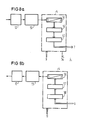
- FIGS. 6 and 7 show the mode of operation of the line connection units 5.
- FIG. 6a shows how 8-bit groups run from the transmission bus data line 7 to the output connection 3b.
- FIG. 6 b shows how 8-bit groups get from the input connection 3 a to the receive bus data line 8.
- the arrangement of Figure 6a includes a code converter 35, additional memory 37a and 37b, eight input memory 38, a counter 4 is 0, a channel allocation memory 42 and the multiplexer and parallel-serial converter 17 with output terminal 3b.
- 8-bit groups arriving on the transmission bus data line 7 are successively fed into input memory 38.
- the respective input memory 38 is selected via a first output 39 of the counter 40.
- One of the 8-bit groups is not in one of the input memories 38 but entered in the additional memory 37a.
- the counter 40 thus sequentially selects one of twenty-eight DS1 input ports 2a for outgoing transmission to the DS3 output port 3b.
- the twenty-ninth time slot enables distribution, monitoring and branching of 8-bit groups by means of the additional memory 37a.
- the counter 40 actuates the additional memory 37a for the transmission of 8-bit groups in this time slot.
- each 8-bit group contains a data byte of a 24-channel PCM signal.
- the counter 40 is now extended by a (1 to 24) counter which continues to count after each passage through the (1 to 29) counter.
- the second output 41 of the counter 40 addresses the channel allocation memory 42 in which 12-bit target addresses are stored in twenty-nine locations for DS1 operation or in six hundred and ninety-six locations for DSO operation. After addressing, the channel allocation memory 42 feeds the selected destination address into the send bus address line 9.
- Each 12-bit destination address is used for transmission from the channel allocation memory 42 via the transmission bus Address line 9 processed by the code converter 35.
- one of sixteen lines is provided in the address lines 9 and 10 for selection of one of sixteen line connection units 4.
- Three further lines identify one of eight connections 2.
- Each line connection unit 5 can then address one of up to one hundred and twenty-eight possible DS1 locations.
- the order of transmission via the bus system 6 is controlled by writing destination addresses into the channel allocation memory 42.
- the contents of its memory locations are regularly applied to the send bus address line 9 via the code converter 35 for the duration of a time slot. It is thus determined for each time slot which 8-bit group is transmitted by a line connection unit 4 via the associated send bus data line 7a, 7b, 7c or 7d. Because this send bus data line is constantly allocated to a specific learning connection unit 5, the destination addresses in the memory locations determine the destination line connection unit 5 and the output connection 3b.
- Each transmit bus data line 7a to 7d transmits at least twenty-eight and preferably twenty-nine DS 1 signals interleaved in time.
- a DS1C signal is divided into two DS1 signals and then connected through in the manner described above.
- FIG. 6b contains a parallel-serial converter and demultiplexer 25 with input connection 3a, twenty-eight output memories 43, a counter 44, a channel assignment memory 45, an additional memory 37b and a code converter 36.
- a DS3 signal applied to the input terminal 3a is broken down in the parallel-serial converter and demultiplexer 25 and supplied to the output memories 43. These are selected by counter 44.
- An 8-bit group is not input into one of the output memories 43 but into the additional memory 37b.
- the counter 44 thus sequentially selects one of twenty-eight DS1 output ports 2b for outgoing transmission. In contrast, in DSO mode, counter 44 sequentially selects one of twenty-four DSO channels.
- the output memories 43 feed the receive bus data line 8 and the channel assignment memory 45 the receive bus address line 10.
- FIG. 7 shows more clearly than FIG. 6a how each DS3 frame is generated by the parallel-serial converter and multipexer 17.
- This receives 8-bit groups of the input memories 38 and inserts the individual bits of the 8-bit groups one after the other. controlled by the DS3 frame synchronizing circuit 46 into a DS3 frame.
- Each of the input memories 38 consists of two sections: an input flip-flop 47 (latch), which is activated by a signal from a decoder 49, and an output flip-flop 48 (latch). It behaves like a buffer memory as used in conventional multiplexers.
- the part of the line connection units 4 which is responsible for the incoming DS3 signals according to FIG. 6b is in principle identical and works in the opposite way to the part just described.
- FIGS. 8a and 8b show the mode of operation of a line connection unit 4.
- the line connection unit 4 receives a destination address with the aid of the send bus address line 9. This causes the line connection unit 4 to put an 8-bit group on the transmission bus data line 7.
- This 8-bit group is a parallel representation of the serial DS1 data which reach the line connection unit 4 through the interface 13.
- a DS1 demultiplexer 50 identifies the individual DSO bytes (8 bits) in the DS1 signal. Since the line connection unit 5 is often presented with a destination address than DSO bytes are available from the line connection unit 4, a "buffer empty" indicator L must keep the line connection unit 5 up to date on the validity of the data on the transmission bus data line 7.
- the line connection unit 4 contains a parallel-to-serial converter 56, buffer memories 57 and 58, in DSO operation additionally a Muftiplexer 55 and an interface 19.
- FIG. 9 shows a Muldex according to the invention with a line connection unit 4 for low bit rate, with a bus system 6 for DSO operation and with a line connection unit 5 for high bit rate.
- the line connection unit 4 contains eight DS 1 demultiplexers and serial-parallel converters 65, only one of which is shown, an addressable read / write memory 59, a data bus interface or data bus driver 61 and an address bus receiver 63 in the transmission direction and in the receive direction a data bus receiver 62, an address bus receiver 64, an addressable read-write memory 60, a logic circuit 67 and eight DS1 multiplexers and parallel-serial converters 66, only one of which is shown.
- the line connection unit 5 contains a parallel-to-serial converter and multiplexer 17, input memory 38, addressable read-write memories 73 and 74, a bus receiver 69, bus drivers 70 to 72, channel assignment memories 42 and 45, serial-to-parallel converter and demuitiplexer 25 and Output storage 43.
- Input storage 38 and output storage 43 are capable of storing six hundred and seventy-two DSO channel data values.
- the line connection unit 4 has already been explained in more detail with reference to FIGS. 8a and 8b and the line connection unit 5 with reference to FIGS. 6a and 6b. Numbers in parentheses indicate the number of parallel wires.
- the line connection unit 4 contains in the addressable read-write memory 59 in addition to the already recommended buffer memory with sufficient elastic storage capacity for storing samples from all demultiplexed DSO channels from all eight DS1 demultiplexers and serial-to-parallel converters 65 or other DSO connections .
- the DSO channel reception is discussed, which is retransmitted to an outgoing DSO channel in the same DS1 signal or another DS1 signal. It is assumed that the DS1 multiplexer / demultiplexer combination shown is assigned to the same DS1 line.
- the line connection unit 5 has stored in its channel assignment memory 42 an address which is assigned to a specific DSO channel (for example one of twenty-four) in a specific DS1 signal in the line connection unit 4. Furthermore, the line connection unit 5 preprogrammed to transfer data from the input memories 38 in such a way that the DSO channel addressed in a specific time slot of the bus system 6 is inserted into specific time slots of the DS3 signal at the output connection 3b.
- the 12-bit destination address is essentially given to the send bus address line 9 via the bus driver 70. While it is being sent to all line connection units 4, only a preselected line connection unit 4 passes the transmitted address to the address bus receiver 63. For this purpose, 4 bits select one of sixteen learning connection units 4, which is carried out with the aid of a module selection line, not shown.
- a specific DS1 signal is identified from eight DS1 signals (from twenty-four DSO channels) by a further 3 bits of information. A further 5 bits are used to select a DSO channel from a specific DS1 signal.
- the DS1 demultiplexer at 65 continuously breaks down a serial data stream into its twenty-four DSO data bytes.
- the serial-to-parallel converter in 65 then converts them into parallel DSO data bytes and adds a parity bit and a stuff bit.
- the twenty-four DSO data bytes with the parity bits and stuff bits are stored in successive address locations in the addressable read-write memory 64.
- the parallel data transmission for a particular DSO channel can contain 14 bits: 8 bits represent a DSO data byte, 4 bit marking bits Sa, Sb, Sc and Sd for extended superframe operation, 1 bit a parity bit and 1 bit a stuff bit.
- the data bus driver 61 outputs 14-bit data which are transmitted by the bus system 6. This data is expected from the bus receiver 69 of the transmission bus data line 7 during the above-mentioned time slot.
- the bus receiver 69 receives these 14 bits in parallel, the 10 bits of data including the parity bit and the stuff bit are supplied by input memories 38 in parallel to the parallel-to-serial converter in FIG. 17 and in series to the multiplexer in FIG. 17.
- A, B, C and D signaling bits (switching technology identifier) in the DSO bytes marked by the marking bits Sa, Sb, Sc and Sd are extracted and into the addressable read-write memory 73 for temporary storage for output delivered in the sixth, twelfth, eighteenth, and twenty-fourth frames of serial data transmission.
- Serial data of a DS3 signal received in the receiving direction at the input terminal 3a are received by the demultiplexer in FIG. 25.
- the serial-to-parallel converter in 25 extracts the DSO data bytes and supplies them, as well as the parity bit and the stuff bit, to the bus driver 72 via the output memories 43.
- the A, B, C and D signaling bits of the sixth, twelfth, eighteenth and Twenty-fourth frames are provided to an A, B, C, and D memory location in addressable random access memory 74 for temporary storage.
- the bus driver 72 supplies the combined 14-bit signal parallel to the receive bus data line 8.
- a 12-bit destination address is sent from the channel allocation memory 4 5 via the bus driver 71 to the receive bus address line 10 and to the individual module selection line already mentioned the fourteen data bits sent which are received by the address bus receiver 64 and the data bus receiver 62.
- the destination address data identify exactly for which DSO channel of the DS1 line the data is intended. These are loaded into the individually addressed memory location of the addressable read-write memory 69.
- the addressable read-write memory 60 outputs the ten data bits and the A, B, C and D signaling bits in parallel when a continuous counter (not shown) in the line connection unit 4 reaches this address. They are first routed to logic shaft 67, the operation of which is controlled by the DS1 multiplexer in 66. This signals logic circuit 67 when the A, B, C and D signaling bits are to be inserted in the sixth, twelfth, eighteenth and twenty-fourth frames at the input of the parallel-to-serial converter in 66. Finally, the DSO data value is provided in the preselected one of twenty-four DSO channel outputs of the DS1 multiplexer at 66.
- a means of connecting, for example, DSO channel # 8 out of twenty-four channels in a single DS1 signal has been presented.
- data of this channel are switched through and multiplexed, for example to DSO channel no. 97 from six hundred and seventy-two channels of a single DS3 signal.
- channel # 8 of twenty-four channels in a DS1 signal can be connected to channel # 3 of twenty-four channels of the same or a different DS1 signal. It is important to recognize that the process is controlled via a line connection unit 5.
- the channels in the direction from channel No. 3 to channel No. 8 and vice versa are controlled by 12-bit destination addresses which are sent out by the line connection unit 5.
- the data are transmitted via the transmission bus data line 7 to the line connection unit 5, stored in the additional memories 37a in FIGS. 6a and 6b and transmitted back to the line connection 4 in a total of two address / data transmission cycles.
- one of the twenty-nine DS1 transmission and reception bus time slots on either the transmission bus data line 7 or the reception bus data line 8 can be routed to a predetermined line connection unit 4 for monitoring, testing or other purposes.
- a signal coming from any line connection unit 4 can be used in any of the twenty-nine DS1 time slots.
- DS1 data can be redirected from a serial-to-parallel converter in 2 5 directly to the parallel-to-serial converter in FIG. 17.
- the sequence of the entire data transmission is determined by the destination addresses stored in the channel allocation memories 42 and 45.
- every component or every unit can be implemented using CMOS technology.
- a line connection unit 4 for low bit rate without DSO operation can be constructed from only two integrated circuit chips for each DS1 signal: one for parallel-serial and serial-parallel conversion, the other for encoder / decoder functions and monitoring .
- the line connection unit 5 for high bit rate can consist of two more fundamental chip chips, while a module with low bit rate requires a different design in DSO operation, but can be constructed from a similar pair of chip chips.
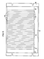
- FIG. 11 shows a device frame 86 for holding several Muldex according to the invention.
- An operating power supply 87, a reserve power supply 88, protective relays 92 upstream of connections 2 and 3 and a printed circuit board are installed in the rear of the device frame 86 in the device frame 86.
- the device frame 86 contains plug-in sockets into which plug-in modules can be inserted which have plug-in contact with the printed circuit board on which the bus system 6 is arranged, among other things.
- the plug-in units 90 belonging to a Muldex with line connecting units 4 , plug-in units 89 with line connecting units 5 and measuring plug-in units 91 are first inserted into the plug-in sockets. In the still free plug-in sockets can be inserted associated with a plug-in 89 bus expansion module 85.
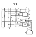
- FIG. 10 shows that a bus expansion module 85 is required for the cooperation of more than four Muldex for each line connection unit 5.
- This contains a DS3 transmitter extension part 80 in the form of an addressable read-write memory and a DS3 receiver extension part 82 also in the form of an addressable read-write memory in order to enable storage of data for two transmission directions of a line connection unit 5 .
- Each of these addressable read-write memories 80 and 82 is used to store six hundred and seventy-two DSO channel data values for each direction of transmission.
- the bus expansion module 85 can be directly addressed by the line connection unit 5 shown.
- the bus expansion module 85 also extends the bus system 6 to other Muldex either via the bus matrix control device 84 or with the aid of direct connections.
- the conductors 81 and 83 can be used to complete the connections. In this way, the capacity of the system described can be greatly expanded and its properties can be increased.
- the bus expansion module 85 comprises a connection 77 to the bus system 6, connections 78 to a transmitter 75 and a receiver 76 in the line connection unit 5, and control line connections 79 from the controlling line connection unit 5.
- FIG. 1 four bus expansion modules 85 are shown, which complement the four plug-in units 89 with line connection units 5 or three plug-in units 89 and a reserve insert 89.
- data is transmitted from the transmission bus data line 7 through a transmitter 76 to the DS3 transmission part 33 and received DS3 data via the receiver 76 to the reception bus data line 8 - in the case of superframe operation which is normally not expanded.
- the transmitter 75 and the receiver 76 are summaries of the bus acceptance, data storage, counting, etc. functions previously described in detail.
- data are introduced in the transmission direction from a line connection unit 4 into the addressable read-write memory 80 via the transmission bus data line 7; in an analogous manner as they are introduced into the line connection unit 5 during normal operation.
- the line connection unit 5 assigned to the bus expansion module 85 is not affected, since the destination of the data is another Muldex.
- the bus matrix control device 84 transmits the data to this device. If data from another Muldex is intended for an output of the line connection unit 5, the data is passed through the DS3 transmission expansion part 80 via a direct connection to the transmitter 75 and to the DS3 transmission part 33.
- the data received in the DS3 receiving part 34 which are normally switched through by the receiver 76 to the receiving bus data line 8, can now be passed on through a direct connection to the DS3 receiver extension part 82 and then to the bus matrix control device 84.
- Data received in the DS3 receiver extension part 82 via the line 83 is output to the receive bus data line 8.
- a line connection unit 4 is unable to determine any difference between this data and that from the receiver 76.
Landscapes
- Engineering & Computer Science (AREA)
- Computer Networks & Wireless Communication (AREA)
- Signal Processing (AREA)
- Computer Hardware Design (AREA)
- Time-Division Multiplex Systems (AREA)
- Amplifiers (AREA)
Priority Applications (1)
| Application Number | Priority Date | Filing Date | Title |
|---|---|---|---|
| AT85116257T ATE67361T1 (de) | 1984-12-20 | 1985-12-19 | Muldex mit kanalverteiler fuer digitalsignale verschiedener hierachiestufen. |
Applications Claiming Priority (4)
| Application Number | Priority Date | Filing Date | Title |
|---|---|---|---|
| US683901 | 1984-12-20 | ||
| US06/683,901 US4685101A (en) | 1984-12-20 | 1984-12-20 | Digital multiplexer for PCM voice channels having a cross-connect capability |
| US758990 | 1985-07-25 | ||
| US06/758,990 US4697262A (en) | 1984-12-20 | 1985-07-25 | Digital carrier channel bus interface module for a multiplexer having a cross-connect bus system |
Publications (3)
| Publication Number | Publication Date |
|---|---|
| EP0186141A2 true EP0186141A2 (fr) | 1986-07-02 |
| EP0186141A3 EP0186141A3 (en) | 1988-08-17 |
| EP0186141B1 EP0186141B1 (fr) | 1991-09-11 |
Family
ID=27103222
Family Applications (1)
| Application Number | Title | Priority Date | Filing Date |
|---|---|---|---|
| EP85116257A Expired - Lifetime EP0186141B1 (fr) | 1984-12-20 | 1985-12-19 | Multiplexeur démultiplexeur avec répartiteur de canaux pour signaux numériques de différents niveaux de hiérarchie |
Country Status (7)
| Country | Link |
|---|---|
| US (1) | US4697262A (fr) |
| EP (1) | EP0186141B1 (fr) |
| AU (1) | AU579543B2 (fr) |
| BR (1) | BR8506380A (fr) |
| CA (1) | CA1289668C (fr) |
| DE (1) | DE3584085D1 (fr) |
| NO (1) | NO172618C (fr) |
Cited By (11)
| Publication number | Priority date | Publication date | Assignee | Title |
|---|---|---|---|---|
| EP0231630A2 (fr) * | 1986-01-22 | 1987-08-12 | Nortel Networks Corporation | Equipement de transmission |
| EP0255255A2 (fr) * | 1986-08-01 | 1988-02-03 | General DataComm, Inc. | Multiplexeur grande vitesse à bits entrelacés et à répartition temporelle pour systèmes de communication multinodaux |
| DE3901557A1 (de) * | 1989-01-20 | 1989-08-10 | Ant Nachrichtentech | Vermittlungseinrichtung fuer digitale multiplexsignale |
| EP0353610A2 (fr) * | 1988-08-05 | 1990-02-07 | Mitsubishi Denki Kabushiki Kaisha | Dispositif de multiplexage |
| DE3901867C1 (en) * | 1989-01-23 | 1990-03-15 | Siemens Ag, 1000 Berlin Und 8000 Muenchen, De | Channel distributor for plesiochronous signals |
| DE3901868C1 (en) * | 1989-01-23 | 1990-03-22 | Siemens Ag, 1000 Berlin Und 8000 Muenchen, De | Channel distributor for plesiochronous signals |
| WO1990016121A1 (fr) * | 1989-06-16 | 1990-12-27 | British Telecommunications Public Limited Company | Noeuds de commutation de donnees |
| EP0425731A1 (fr) * | 1989-11-03 | 1991-05-08 | Siemens Aktiengesellschaft | Dispositif de commande d'un système à bus pour un multiplexeur programmable et flexible de signaux numériques |
| WO1991014320A1 (fr) * | 1990-03-06 | 1991-09-19 | Siemens-Albis Ag | Multiplexeur de signaux numeriques |
| FR2681998A1 (fr) * | 1991-09-26 | 1993-04-02 | Alcatel Telspace | Procede et dispositif pour l'elaboration des signaux synchronises necessaires au traitement de la justification et/ou de la dejustification dans une transmission numerique d'affluent secondaire. |
| US5425022A (en) * | 1989-06-16 | 1995-06-13 | British Telecommunications Public Limited Company | Data switching nodes |
Families Citing this family (16)
| Publication number | Priority date | Publication date | Assignee | Title |
|---|---|---|---|---|
| JPS6128235A (ja) * | 1984-07-18 | 1986-02-07 | Nec Corp | 表示付無線選択呼出受信機 |
| NL8503476A (nl) * | 1985-12-18 | 1987-07-16 | Philips Nv | Bussysteem. |
| US5033064A (en) * | 1988-12-09 | 1991-07-16 | Transwitch Corporation | Clock dejitter circuit for regenerating DS1 signal |
| US5040170A (en) * | 1988-12-09 | 1991-08-13 | Transwitch Corporation | System for cross-connecting high speed digital signals |
| US4967405A (en) * | 1988-12-09 | 1990-10-30 | Transwitch Corporation | System for cross-connecting high speed digital SONET signals |
| US5142529A (en) * | 1988-12-09 | 1992-08-25 | Transwitch Corporation | Method and means for transferring a data payload from a first SONET signal to a SONET signal of different frequency |
| US5423021A (en) * | 1989-11-03 | 1995-06-06 | Compaq Computer Corporation | Auxiliary control signal decode using high performance address lines |
| JPH07123067A (ja) * | 1993-10-20 | 1995-05-12 | Hitachi Ltd | 多重化装置 |
| JP3408720B2 (ja) * | 1996-06-13 | 2003-05-19 | 富士通株式会社 | 高速同期多重化装置 |
| US5951659A (en) * | 1997-04-07 | 1999-09-14 | Ncr Corporation | Communications-oriented computer system backplane including a PCI input/output bus for transmission of address, data, and control information, and a time-domain multiplexed signal bus (TDMSB) for transmission of high-speed digitized signal information |
| US6425041B1 (en) * | 1998-06-05 | 2002-07-23 | Micron Technology, Inc. | Time-multiplexed multi-speed bus |
| US6292463B1 (en) * | 1998-07-06 | 2001-09-18 | Alcatel Canada Inc. | Method and apparatus for recovering from a signalling failure in a switched connection data transmission network |
| US6654822B1 (en) * | 2000-06-28 | 2003-11-25 | Intel Corporation | Cascadable cross connect architecture |
| US6707816B1 (en) | 2000-06-29 | 2004-03-16 | Intel Corporation | Integrated signaling / payload cross connect architecture |
| US7436954B2 (en) | 2001-02-28 | 2008-10-14 | Cavium Networks, Inc. | Security system with an intelligent DMA controller |
| JP5659910B2 (ja) * | 2011-03-29 | 2015-01-28 | 富士通株式会社 | フレームマッピング装置及びフレームマッピング方法 |
Citations (1)
| Publication number | Priority date | Publication date | Assignee | Title |
|---|---|---|---|---|
| DE3228518A1 (de) * | 1982-07-29 | 1984-02-09 | Heinrich-Hertz-Institut für Nachrichtentechnik Berlin GmbH, 1000 Berlin | Schaltungsanordnung zur aufbereitung von pcm-systemen zum zwecke der vermittlung |
Family Cites Families (5)
| Publication number | Priority date | Publication date | Assignee | Title |
|---|---|---|---|---|
| US4383315A (en) * | 1981-07-20 | 1983-05-10 | Bell Telephone Laboratories, Incorporated | Idle time slot seizure and transmission facilities for loop communication system |
| SE430288B (sv) * | 1982-02-24 | 1983-10-31 | Ellemtel Utvecklings Ab | Telekommunikationssystem for overforing av datainformation medelst en digital vexel |
| JPS5913443A (ja) * | 1982-07-14 | 1984-01-24 | Fuji Xerox Co Ltd | 非同期接続装置 |
| FR2538984A1 (fr) * | 1982-12-30 | 1984-07-06 | Devault Michel | Commutateur pour reseau numerique multidebit a commutation temporelle asynchrone adapte aux videocommutations |
| US5436872A (en) * | 1994-06-27 | 1995-07-25 | Westinghouse Elec Corp | Time delay-phase shift combination beamformer |
-
1985
- 1985-07-25 US US06/758,990 patent/US4697262A/en not_active Expired - Fee Related
- 1985-12-18 CA CA000497970A patent/CA1289668C/fr not_active Expired - Fee Related
- 1985-12-19 BR BR8506380A patent/BR8506380A/pt not_active IP Right Cessation
- 1985-12-19 DE DE8585116257T patent/DE3584085D1/de not_active Expired - Fee Related
- 1985-12-19 EP EP85116257A patent/EP0186141B1/fr not_active Expired - Lifetime
- 1985-12-19 AU AU51467/85A patent/AU579543B2/en not_active Ceased
- 1985-12-20 NO NO855193A patent/NO172618C/no unknown
Patent Citations (1)
| Publication number | Priority date | Publication date | Assignee | Title |
|---|---|---|---|---|
| DE3228518A1 (de) * | 1982-07-29 | 1984-02-09 | Heinrich-Hertz-Institut für Nachrichtentechnik Berlin GmbH, 1000 Berlin | Schaltungsanordnung zur aufbereitung von pcm-systemen zum zwecke der vermittlung |
Non-Patent Citations (2)
| Title |
|---|
| NATIONAL TELECOMMUNICATIONS CONFERENCE, New Orleans, 29. November - 3. Dezember 1981, Seiten B1.2.1 - B1.2.7, IEEE; R.P. ABBOTT et al.: "Digital access and cross-connect system - system architecture" * |
| PROSPEKT VON SIEMENS AG, Bestell.-Nr. S42023-A750-A1-1-29; "Digitalsignal-Kanalverteiler DKVt2" * |
Cited By (16)
| Publication number | Priority date | Publication date | Assignee | Title |
|---|---|---|---|---|
| EP0231630A3 (en) * | 1986-01-22 | 1989-06-14 | Stc Plc | Data transmission equipment |
| EP0231630A2 (fr) * | 1986-01-22 | 1987-08-12 | Nortel Networks Corporation | Equipement de transmission |
| EP0255255A2 (fr) * | 1986-08-01 | 1988-02-03 | General DataComm, Inc. | Multiplexeur grande vitesse à bits entrelacés et à répartition temporelle pour systèmes de communication multinodaux |
| EP0255255A3 (en) * | 1986-08-01 | 1990-01-17 | General Datacomm, Inc. | High speed bit interleaved time division multiplexer for multinode communication systems |
| EP0353610A3 (fr) * | 1988-08-05 | 1991-07-17 | Mitsubishi Denki Kabushiki Kaisha | Dispositif de multiplexage |
| EP0353610A2 (fr) * | 1988-08-05 | 1990-02-07 | Mitsubishi Denki Kabushiki Kaisha | Dispositif de multiplexage |
| DE3901557A1 (de) * | 1989-01-20 | 1989-08-10 | Ant Nachrichtentech | Vermittlungseinrichtung fuer digitale multiplexsignale |
| DE3901867C1 (en) * | 1989-01-23 | 1990-03-15 | Siemens Ag, 1000 Berlin Und 8000 Muenchen, De | Channel distributor for plesiochronous signals |
| DE3901868C1 (en) * | 1989-01-23 | 1990-03-22 | Siemens Ag, 1000 Berlin Und 8000 Muenchen, De | Channel distributor for plesiochronous signals |
| WO1990016121A1 (fr) * | 1989-06-16 | 1990-12-27 | British Telecommunications Public Limited Company | Noeuds de commutation de donnees |
| US5425022A (en) * | 1989-06-16 | 1995-06-13 | British Telecommunications Public Limited Company | Data switching nodes |
| WO1991007031A1 (fr) * | 1989-11-03 | 1991-05-16 | Siemens Aktiengesellschaft | Bus controleur pour un multiplexeur de signaux numeriques souple et programmable |
| EP0425731A1 (fr) * | 1989-11-03 | 1991-05-08 | Siemens Aktiengesellschaft | Dispositif de commande d'un système à bus pour un multiplexeur programmable et flexible de signaux numériques |
| WO1991014320A1 (fr) * | 1990-03-06 | 1991-09-19 | Siemens-Albis Ag | Multiplexeur de signaux numeriques |
| CH679820A5 (fr) * | 1990-03-06 | 1992-04-15 | Siemens Ag Albis | |
| FR2681998A1 (fr) * | 1991-09-26 | 1993-04-02 | Alcatel Telspace | Procede et dispositif pour l'elaboration des signaux synchronises necessaires au traitement de la justification et/ou de la dejustification dans une transmission numerique d'affluent secondaire. |
Also Published As
| Publication number | Publication date |
|---|---|
| AU579543B2 (en) | 1988-11-24 |
| AU5146785A (en) | 1986-06-26 |
| DE3584085D1 (de) | 1991-10-17 |
| NO172618B (no) | 1993-05-03 |
| BR8506380A (pt) | 1986-09-02 |
| CA1289668C (fr) | 1991-09-24 |
| NO855193L (no) | 1986-06-23 |
| EP0186141A3 (en) | 1988-08-17 |
| US4697262A (en) | 1987-09-29 |
| NO172618C (no) | 1993-08-11 |
| EP0186141B1 (fr) | 1991-09-11 |
Similar Documents
| Publication | Publication Date | Title |
|---|---|---|
| EP0186141B1 (fr) | Multiplexeur démultiplexeur avec répartiteur de canaux pour signaux numériques de différents niveaux de hiérarchie | |
| DE69028863T2 (de) | Formatumsetzer | |
| EP0320772A3 (fr) | Procédé pour la commutation hybride de paquets et dispositifs à cet effet | |
| EP0024708B1 (fr) | Multiple de canaux temporels pour un système à multiplexage temporel pour la commutation de signaux numériques, en particulier de messages à modulation en delta | |
| EP0514856B1 (fr) | Réseau de commutation pour commuter des canaux | |
| DE2848249A1 (de) | Digitale vermittlungsanordnung | |
| DE68924191T2 (de) | Für integrierte Schaltungsausführung geeignete Paketvermittlung. | |
| EP0598455B1 (fr) | Système de transmission pour la hiérarchie numérique synchrone | |
| DE69220402T2 (de) | ATM-Zellenmultiplexeinrichtung zur Reduzierung der Zugriffsgeschwindigkeit für einen FIFO-Speicher | |
| EP0705507B1 (fr) | Procede permettant de convertir des flux de donnees numeriques avec une structure a cellules a mode de transfert asynchrone (mta) | |
| DE2148994C2 (de) | Verfahren zur Vermittlung von PCM Si gnalen eines PCM Zeitmultiplex Fernmeldenetzes | |
| EP0005157A2 (fr) | Réseau de couplage à groupage à rebroussement avec plusieurs étages pour un central de commutation MIC | |
| DE19627728A1 (de) | Netzelement und Ein-/Ausgabeeinheit für ein synchrones Übertragungssystem | |
| EP0185936A2 (fr) | Montage de circuit d'interface pour la connexion de sources de données avec récepteurs de données et systèmes de commutation avec de tels montages de circuit d'interface | |
| DE3816747A1 (de) | Leistungsvermittelnde paket-vermittlungseinrichtung | |
| EP0110360B1 (fr) | Montage de circuit pour rassembler et séparer des signaux de parole et des données lors de la transmission à travers un réseau de commutation numérique | |
| EP0434629B1 (fr) | Méthode et circuit de traitement d'information de signalisation dans des multiplexeurs | |
| DE2512047A1 (de) | Anordnung zur serienparallelwandlung, insbesondere fuer zeitvielfachvermittlungsanlagen | |
| EP0395780A1 (fr) | Multiplexeur flexible | |
| EP1217867A2 (fr) | Dispositif de brassage pour commutation arbitraire des signaux de communication entre des planes de multiplexage différentes | |
| EP1217869A2 (fr) | Dispositif de brassage pour commutation arbitraire des signaux de communication entre des planes de multiplexage différentes | |
| DE2451837A1 (de) | Verfahren zur bildung und aufloesung eines multiplexes aus mehreren datenkanaelen in einer durchschalteeinheit einer pcm-zeitmultiplex-fernmeldevermittlungsanlage | |
| DE3783149T2 (de) | Tst-typ-vermittlungssystem fuer breitbandvermittlung. | |
| EP1217868A2 (fr) | Dispositif de brassage pour commutation arbitraire des signaux de commutation entre des planes de multiplexage différentes | |
| CH624806A5 (en) | Arrangement for central generation of an envelope-interleaved time division multiplex signal |
Legal Events
| Date | Code | Title | Description |
|---|---|---|---|
| PUAI | Public reference made under article 153(3) epc to a published international application that has entered the european phase |
Free format text: ORIGINAL CODE: 0009012 |
|
| AK | Designated contracting states |
Kind code of ref document: A2 Designated state(s): AT BE CH DE FR GB IT LI NL SE |
|
| PUAL | Search report despatched |
Free format text: ORIGINAL CODE: 0009013 |
|
| AK | Designated contracting states |
Kind code of ref document: A3 Designated state(s): AT BE CH DE FR GB IT LI NL SE |
|
| 17P | Request for examination filed |
Effective date: 19890208 |
|
| 17Q | First examination report despatched |
Effective date: 19910121 |
|
| GRAA | (expected) grant |
Free format text: ORIGINAL CODE: 0009210 |
|
| AK | Designated contracting states |
Kind code of ref document: B1 Designated state(s): AT BE CH DE FR GB IT LI NL SE |
|
| REF | Corresponds to: |
Ref document number: 67361 Country of ref document: AT Date of ref document: 19910915 Kind code of ref document: T |
|
| REF | Corresponds to: |
Ref document number: 3584085 Country of ref document: DE Date of ref document: 19911017 |
|
| ET | Fr: translation filed | ||
| ITF | It: translation for a ep patent filed | ||
| GBT | Gb: translation of ep patent filed (gb section 77(6)(a)/1977) | ||
| PLBE | No opposition filed within time limit |
Free format text: ORIGINAL CODE: 0009261 |
|
| STAA | Information on the status of an ep patent application or granted ep patent |
Free format text: STATUS: NO OPPOSITION FILED WITHIN TIME LIMIT |
|
| 26N | No opposition filed | ||
| PGFP | Annual fee paid to national office [announced via postgrant information from national office to epo] |
Ref country code: AT Payment date: 19941123 Year of fee payment: 10 |
|
| PGFP | Annual fee paid to national office [announced via postgrant information from national office to epo] |
Ref country code: BE Payment date: 19941213 Year of fee payment: 10 |
|
| EAL | Se: european patent in force in sweden |
Ref document number: 85116257.8 |
|
| PGFP | Annual fee paid to national office [announced via postgrant information from national office to epo] |
Ref country code: CH Payment date: 19950317 Year of fee payment: 10 |
|
| PG25 | Lapsed in a contracting state [announced via postgrant information from national office to epo] |
Ref country code: AT Effective date: 19951219 |
|
| PG25 | Lapsed in a contracting state [announced via postgrant information from national office to epo] |
Ref country code: LI Effective date: 19951231 Ref country code: CH Effective date: 19951231 Ref country code: BE Effective date: 19951231 |
|
| PGFP | Annual fee paid to national office [announced via postgrant information from national office to epo] |
Ref country code: DE Payment date: 19960219 Year of fee payment: 11 |
|
| BERE | Be: lapsed |
Owner name: SIEMENS A.G. Effective date: 19951231 |
|
| REG | Reference to a national code |
Ref country code: CH Ref legal event code: PL |
|
| PGFP | Annual fee paid to national office [announced via postgrant information from national office to epo] |
Ref country code: GB Payment date: 19961118 Year of fee payment: 12 |
|
| PGFP | Annual fee paid to national office [announced via postgrant information from national office to epo] |
Ref country code: SE Payment date: 19961210 Year of fee payment: 12 |
|
| PGFP | Annual fee paid to national office [announced via postgrant information from national office to epo] |
Ref country code: NL Payment date: 19961217 Year of fee payment: 12 |
|
| PGFP | Annual fee paid to national office [announced via postgrant information from national office to epo] |
Ref country code: FR Payment date: 19961223 Year of fee payment: 12 |
|
| PG25 | Lapsed in a contracting state [announced via postgrant information from national office to epo] |
Ref country code: DE Effective date: 19970902 |
|
| PG25 | Lapsed in a contracting state [announced via postgrant information from national office to epo] |
Ref country code: GB Free format text: LAPSE BECAUSE OF NON-PAYMENT OF DUE FEES Effective date: 19971219 |
|
| PG25 | Lapsed in a contracting state [announced via postgrant information from national office to epo] |
Ref country code: SE Free format text: LAPSE BECAUSE OF NON-PAYMENT OF DUE FEES Effective date: 19971220 |
|
| PG25 | Lapsed in a contracting state [announced via postgrant information from national office to epo] |
Ref country code: FR Free format text: THE PATENT HAS BEEN ANNULLED BY A DECISION OF A NATIONAL AUTHORITY Effective date: 19971231 |
|
| PG25 | Lapsed in a contracting state [announced via postgrant information from national office to epo] |
Ref country code: NL Free format text: LAPSE BECAUSE OF NON-PAYMENT OF DUE FEES Effective date: 19980701 |
|
| GBPC | Gb: european patent ceased through non-payment of renewal fee |
Effective date: 19971219 |
|
| NLV4 | Nl: lapsed or anulled due to non-payment of the annual fee |
Effective date: 19980701 |
|
| EUG | Se: european patent has lapsed |
Ref document number: 85116257.8 |
|
| REG | Reference to a national code |
Ref country code: FR Ref legal event code: ST |