EP0186141A2 - Multiplexer demultiplexer with a channel distributor for digital signals of different hierarchical levels - Google Patents
Multiplexer demultiplexer with a channel distributor for digital signals of different hierarchical levels Download PDFInfo
- Publication number
- EP0186141A2 EP0186141A2 EP85116257A EP85116257A EP0186141A2 EP 0186141 A2 EP0186141 A2 EP 0186141A2 EP 85116257 A EP85116257 A EP 85116257A EP 85116257 A EP85116257 A EP 85116257A EP 0186141 A2 EP0186141 A2 EP 0186141A2
- Authority
- EP
- European Patent Office
- Prior art keywords
- bus
- address
- data
- muldex
- bit rate
- Prior art date
- Legal status (The legal status is an assumption and is not a legal conclusion. Google has not performed a legal analysis and makes no representation as to the accuracy of the status listed.)
- Granted
Links
Images


Classifications
-
- H—ELECTRICITY
- H04—ELECTRIC COMMUNICATION TECHNIQUE
- H04J—MULTIPLEX COMMUNICATION
- H04J3/00—Time-division multiplex systems
- H04J3/16—Time-division multiplex systems in which the time allocation to individual channels within a transmission cycle is variable, e.g. to accommodate varying complexity of signals, to vary number of channels transmitted
- H04J3/1605—Fixed allocated frame structures
- H04J3/1623—Plesiochronous digital hierarchy [PDH]
- H04J3/1641—Hierarchical systems
-
- H—ELECTRICITY
- H04—ELECTRIC COMMUNICATION TECHNIQUE
- H04J—MULTIPLEX COMMUNICATION
- H04J3/00—Time-division multiplex systems
- H04J3/02—Details
- H04J3/06—Synchronising arrangements
- H04J3/062—Synchronisation of signals having the same nominal but fluctuating bit rates, e.g. using buffers
- H04J3/0626—Synchronisation of signals having the same nominal but fluctuating bit rates, e.g. using buffers plesiochronous multiplexing systems, e.g. plesiochronous digital hierarchy [PDH], jitter attenuators
- H04J3/0629—Synchronisation of signals having the same nominal but fluctuating bit rates, e.g. using buffers plesiochronous multiplexing systems, e.g. plesiochronous digital hierarchy [PDH], jitter attenuators in a network, e.g. in combination with switching or multiplexing, slip buffers
Landscapes
- Engineering & Computer Science (AREA)
- Computer Networks & Wireless Communication (AREA)
- Signal Processing (AREA)
- Computer Hardware Design (AREA)
- Time-Division Multiplex Systems (AREA)
- Amplifiers (AREA)
Abstract
Muldex mit mehreren Leitungsanschlußeinheiten (4) niedriger Bitrate und wenigstens einer Leitungsanschlußeinheit (5) hoher Bitrate, die durch ein Koppelfeld in Form eines Bussystems (6) miteinander verbunden sind. Da alle Leitungsanschlußeinheiten (4,5) Multiplexer (17,66) und Demulti-plexer (25,65) enthalten, können Kanäle von Digitalsignalen (DS0,DS1,DS1C,DS2,DS3) verschiedener Hierarchiestufen beliebig durchgeschaltet und umverteilt werden. Eine Zusammenschaltung und ein Zusammenwirken verschiedener Muldex ist möglich.Muldex with several line connection units (4) of low bit rate and at least one line connection unit (5) of high bit rate, which are interconnected by a switching matrix in the form of a bus system (6). Since all line connection units (4, 5) contain multiplexers (17, 66) and demultiplexers (25, 65), channels of digital signals (DS0, DS1, DS1C, DS2, DS3) of different hierarchical levels can be switched through and redistributed as desired. Interconnection and interaction of different Muldex is possible.
Description
Die Erfindung bezieht sich auf ein Muldex mit ersten Anschlüssen für ankommende und abgehende Digitalsignale niedriger Bitrate, mit zweiten Anschlüssen für ankommende und abgehende Digitalsignale hoher Bitrate, mit einem zwischen den ersten und den zweiten Anschlüssen angeordneten MultiplexerlDemultiplexer, mit ersten Schnittstellen zwischen den ersten Anschlüssen und den Anschlüssen niedriger Bitrate des Multiplexer/Demultiplexers und mit zweiten Schnittstellen zwischen den Anschlüssen hoher Bitrate des Multiplexers/Demultiplexers und den zweiten Anschlüssen..The invention relates to a Muldex with first connections for incoming and outgoing digital signals of low bit rate, with second connections for incoming and outgoing digital signals of high bit rate, with a multiplexer demultiplexer arranged between the first and the second connections, with first interfaces between the first connections and the Low bit rate connections of the multiplexer / demultiplexer and with second interfaces between the high bit rate connections of the multiplexer / demultiplexer and the second connections.
Muldex ist die Kurzbezeichnung für ein Multiplexer und Demultiplexer enthaltendes Gerät Unter niedriger und hoher Bitrate sind Bitraten unterschiedlicher Hierarchiestufen zu verstehen.Muldex is the short name for a device containing multiplexers and demultiplexers. Low and high bit rates are understood to mean bit rates of different hierarchical levels.
Die infragekommenden Digitalsignale gehören insbesondere zu den verschiedenen Hierarchiesystemen, die in der Zeitschrift "telcom report", 2 (1979) Beiheft Digital- Übertragungstechnik, Seiten 16 - 20, insbesondere Tabelle 1 dargestellt sind. Multiplexer und Demultiplexer sind in derselben Druckschrift auf den Seiten 59 - 64 beschrieben.The digital signals that come into question belong in particular to the various hierarchy systems which are shown in the journal "telcom report", 2 (1979) supplement digital transmission technology, pages 16-20, especially Table 1. Multiplexers and demultiplexers are described in the same publication on pages 59-64.
Die nordamerikanischen Normen für Digitalsignal-Multiplexer, die DS1-, DS1C- und DS2-Signale in DS3-Signale umsetzen, sind in der Bell-Druckschrift "Digital Multiplexers Requirements and Objectivs", Direktor - Exchange Systems Design, AT&T, 1982, dargestellt und besprochen. Die nachfolgende Tabelle zeigt diese Signale mit ihrer Sprachkanalzahl und ihrer Übertragungs-Bitrate.

Ein DSO-Kanal kann in jeder Übertragungsrichtung achttausend 8-bit-Gruppen von Sprache oder Daten pro Sekunde senden und empfangen. Vierundzwanzig DSO-Kanäle können wiederum zu einem DS1-Kanal zusammengefaßt werden. Dabei werden je eine 8-bit-Gruppe der vierundzwanzig DSO-Kanäle und ein einzelnes Rahmenkennungsbit in einen 193-bit-Rahmen eingefügt.A DSO channel can send and receive eight thousand 8-bit groups of voice or data per second in each direction of transmission. Twenty-four DSO channels can in turn be combined into one DS1 channel. An 8-bit group of the twenty-four DSO channels and a single frame identifier bit are inserted into a 193-bit frame.
Zur nordamerikanischen Hierarchie gehören M13-Multiplexer, die achtundzwanzig DS1-Signale in ein DS3-Signal umsetzen. Dies wird mittels sieben M12-Multiplexem erreicht, von denen jeder vier DS1-Signale in ein DS2-Signal überführt. Ein M23-Multiplexer setzt die sieben DS2-Signale wiederum in ein DS3-Signal um.The North American hierarchy includes M13 multiplexers that convert twenty-eight DS1 signals into a DS3 signal. This is achieved by means of seven M12 multiplexers, each of which converts four DS1 signals into one DS2 signal. An M23 multiplexer converts the seven DS2 signals into a DS3 signal.
Zusätzliche Flexibilität wird durch einen sogenannten MX3-Multiplexer erreicht, der eine verschiedene Anzahl von DS1-, DS1C- und DS2-Signale in ein einziges DS3-Signal umsetzen kann. Beispielsweise können an die Eingänge eines M23-Multiplexers entweder vier zusammengefaßte DS1-Signale, zwei zusammengefaßte DS1C-Signale oder DS2-Signale angelegt werden.Additional flexibility is achieved by a so-called MX3 multiplexer, which can convert a different number of DS 1 , DS 1 C and DS2 signals into a single DS3 signal. For example, either four combined DS1 signals, two combined DS1C signals or DS2 signals can be applied to the inputs of an M23 multiplexer.
Unter der Bezeichnung "DACS" (Digital Access and Cross Connect System) der Firma AT&T Technologies Inc. ist ein digitales Verteilersystem bekanntgeworden, welches zwischen eine veränderbare Anzahl von DS1- und DS1C-Leitungen über Eingänge und Ausgänge geschaltet ist und jeden Sprachkanal einer Leitung mit einem Sprachkanal auf einer anderen Leitung zu verbinden vermag. Dieses System arbeitet in der Art einer Telefonvermittlung. Es enthält einen Koppelpunktbereich, um eine beliebige DS1-oder DS1C-Leitung mit einer anderen DS1- oder DSlC-Leitung zu verbinden. Das System kann kein Multiplexen auf der DS2-oder DS3-Ebene ausführen.A digital distribution system has become known under the name "DACS" (Digital Access and Cross Connect System) from AT&T Technologies Inc., which is connected between a variable number of DS 1 and DS1C lines via inputs and outputs and each voice channel of a line can connect to a voice channel on another line. This system works like a telephone exchange. It contains a cross-point region to any DS1 or DS1C line with another DS1 or DS l C-line to be connected. The system cannot perform multiplexing at the DS2 or DS3 level.
Eine einzelne Umsetzung von einer Bitrate auf eine andere kann durch eine Mehrzahl einzelner MX3-Multiplexer bewirkt werden. Außerdem können auch M12- und MC2- Multiplexer zur Umsetzung auf eineA single conversion from one bit rate to another can be effected by a plurality of individual MX3 multiplexers. In addition, M12 and MC2 multiplexers can also be converted to one
DS2-Bitrate dienen. Während Multfplexgeräte dieser Art auf Sprachübertragungs-Netzknoten besonderer Konfiguration zugeschnitten werden können, sind sie nicht leicht zu programmieren, so daß Änderungen in der Knotenkonfiguration teuer und zeitraubend sind. Das bekannte Gerät beinhaltet eine bestimmte Multiplexer-Hardware, die jedesmal in das System ein- und aus diesem wieder ausgebaut werden muß, wenn eine Änderung durchzuführen ist.Serve DS2 bit rate. While multiplexing devices of this type can be tailored to special configuration voice transmission network nodes, they are not easy to program, so changes in the node configuration are expensive and time consuming. The known device contains a certain multiplexer hardware, which must be installed in and removed from the system each time a change is to be made.
Aufgabe der Erfindung ist es, ein Muldex zu realisieren, in dem eine Kanalverteilung auf verschiedene Hierarchiestufen vorgenommen werden kann.The object of the invention is to implement a Muldex in which a channel distribution can be carried out on different hierarchical levels.
Ausgehend von einem Muldex der einleitend geschilderten Art wird diese Aufgabe erfindungsgemäß dadurch gelöst, daß zwischen den ersten Schnittstellen und dem Multiplexer/Demultiplexer ein Koppelfeld mit einer Koppelfeldsteuerung für eine Kanalverteilung vorgesehen sind.Starting from a Muldex of the type described in the introduction, this object is achieved according to the invention in that a switching matrix with a switching matrix control for a channel distribution is provided between the first interfaces and the multiplexer / demultiplexer.
Bei einer vorteilhaften Ausführungsform sind Sendebus-Datenleitungen, Empfangsbus-Datenleitungen, Sendebus-Adressenleitungen, Empfangsbus-Adressenleitungen und Busanschlußeinrichtungen mit Speicher und Speichersteuerung vorgesehen.In an advantageous embodiment, send bus data lines, receive bus data lines, send bus address lines, receive bus address lines and bus connection devices with memory and memory controller are provided.
Vorteilhaft ist es dabei, wenn in den ersten Busanschlußeinrichtungen ein Demultiplexer und ein Seriell-Parallel-Umsetzer und ein diesem nachgeschalteter erster adressierbarer Schreib-Lese-Speicher (RAM) zur Aufnahme von Daten aus einem Digitalsignal niederer Bitrate und von Adressen vorgesehen sind und wenn in den zweiten Busanschlußeinrichtungen ein zweiter adressierbarer Schreib-Lese-Speicher (RAM) zur Aufnahme von Daten aus einem Digitalsignal hoher Bitrate und von Adressen sowie ein diesem nachgeschalteter Parallel-Seriell-Umsetzer und Multiplexer vorgesehen sind.It is advantageous if a demultiplexer and a serial-to-parallel converter and a downstream first addressable read-write memory (RAM) for receiving data from a low bit rate digital signal and addresses are provided in the first bus connection devices and if in the second bus connection devices are provided with a second addressable read-write memory (RAM) for receiving data from a high bit rate digital signal and addresses, and a parallel-serial converter and multiplexer connected downstream of the latter.
Dabei ist es wiederum vorteilhaft, wenn im ersten adressierbaren Schreib-Lese-Speicher (RAM) eine bestimmte Adresse wenigstens ein bestimmtes Byte aus einem bestimmten Zeitkanal enthält und wenn im zweiten adressierbaren Schreib-Lese-Speicher (RAM) ein bestimmtes Byte für eine Übertragung zu einem bestimmten Zeitkanal gemäß der Adressensignalisierung bereitgestellt wird.It is again advantageous if in the first addressable read / write memory (RAM) a certain address contains at least one certain byte from a certain time channel and if in the second addressable read / write memory (RAM) a certain byte for transmission a certain time channel is provided according to the address signaling.
In den ersten Busanschlußeinrichtungen sind vorteilhafterweise ein Bustreiber an den Sendebus-Datenleitungen und ein erster Adressenbusempfänger und in den zweiten Busanschlußeinrichtungen ein zweiter Adressenbusempfänger und ein Datenbusempfänger vorgesehen, der Bytes in den zweiten adressierbaren Schreib-Lese-Speicher (RAM) in Plätze einspeist, die vom zweiten Adressenbusempfänger angegeben wurden.In the first bus connection devices, a bus driver is advantageously provided on the transmission bus data lines and a first address bus receiver, and in the second bus connection devices a second address bus receiver and a data bus receiver are provided, which feeds bytes into the second addressable read-write memory (RAM) into locations which are provided by the second address bus receiver were specified.
Vorteilhaft ist es weiterhin, wenn in der zweiten Busanschlußeinrichtung zwischen dem zweiten adressierbaren Schreib-Lese-Speicher (RAM) und dem Parallel-Seriell-Umsetzer und Multiplexer eine logische Schaltung vorgesehen ist, die einem rahmensynchronen Einsetzen von Signalisierungsbits in den Datenstrom dient.It is furthermore advantageous if a logic circuit is provided in the second bus connection device between the second addressable read / write memory (RAM) and the parallel-serial converter and multiplexer, which serves for the frame-synchronous insertion of signaling bits in the data stream.
Für den praktischen Betrieb ist es vorteilhaft, wenn ein Gehäuse für einsteckbare Baugruppen vorgesehen ist, wenn an der Gehäuserückwand eine Leiterplatte mit wenigstens Sende- und Empfangbusleitungen vorgesehen ist und wenn Steckverbindungen zur elektrischen und mechanischen Verbindung der Baugruppen mit der Leiterplatte vorgesehen sind.For practical operation, it is advantageous if a housing is provided for plug-in modules, if a printed circuit board with at least transmit and receive bus lines is provided on the rear wall of the housing and if plug connections are provided for the electrical and mechanical connection of the modules to the printed circuit board.
In Weiterbildung der Erfindung ist es vorteilhaft, wenn das Gehäuse für die Aufnahme mehrerer Muldex vorgesehen ist. wenn jeder Leitungsanschlußeinheit für hohe Bitrate eine Buserweiterungs-Baugruppe zugeordnet ist, wenn in der Buserweiterungs-Baugruppe ein mit der Sendebus-Datenleitung und der Sendebus-Adressenleitung verbundener Sender-Erweiterungsteil für hohe Bitrate vorgesehen ist, wenn in der Buserweiterungs-Baugruppe ein mit der Empfangsbus-Datenleitung und der Empfangsbus-Adressenleitung verbundener Empfänger-Erweiterungsteil für hohe Bitrate vorgesehen ist, wenn eine mit dem Sender-Erweiterungsteil und dem Empfänger-Erweiterungsteil verbundene Busmatrix-Kontrolleinrichtung vorgesehen ist und wenn Schalter vorgesehen sind, über die die Busmatrix-Kontrollschaltung die Zuleitung zu den Sende- und Empfangsbusleitungen schließen oder öffnen kann.In a further development of the invention, it is advantageous if the housing is intended to accommodate several Muldex. if a bus expansion module is assigned to each line connection unit for high bit rate, if a transmitter expansion part for high bit rate connected to the send bus data line and the send bus address line is provided in the bus expansion module, if one to the receive bus in the bus expansion module -Datenleitung and the receiving bus address line connected receiver extension part is provided for high bit rate when connected to the transmitter-Erwe i esterification part and the receiver extension part bus matrix control device is provided and if switches are provided via which the bus matrix control circuit, the Can close or open supply line to the send and receive bus lines.
Wenn bisher insbesondere von den nordamerikanischen DS-Signalen die Rede war, so gilt das Gesagte entsprechend für Signale mit europäischer Bitrate und europäische Multiplexer und Demultiplexer sowie sonstige Bitraten und Geräte.If previously there was talk of the North American DS signals in particular, what has been said applies accordingly to signals with a European bit rate and European multiplexers and demultiplexers as well as other bit rates and devices.
Anhand von Ausführungsbeispielen wird die Erfindung nachstehend näher erläutert.The invention is explained in more detail below on the basis of exemplary embodiments.
- Figur 1 zeigt das Blockschaltbild einer Anordnung, die mehrere erfindungsgemäße Muldex umfaßt,FIG. 1 shows the block diagram of an arrangement which comprises several Muldex according to the invention,
- Figur 2 zeigt die Anordnung nach Figur 1 mit einer detaillierten Darstellung des zum Koppelfeld gehörenden Bussystems,FIG. 2 shows the arrangement according to FIG. 1 with a detailed illustration of the bus system belonging to the switching matrix,
- Figur 3 zeigt eine Anordnung zum Multiplexen von vier DS1-Signalen zu bis zu vier DS3-Signalen,FIG. 3 shows an arrangement for multiplexing four DS 1 signals to up to four DS3 signals,
- Figur 4 zeigt eine Anordnung zum Demultiplexen von vier DSt-Signalen aus bis zu vier DS3-Signalen,FIG. 4 shows an arrangement for demultiplexing four DSt signals from up to four DS3 signals,
- Figur 5 zeigt detailliert den Anschluß von Leitungsanschlußeinheiten für hohe und niedrige Bitrate an das Bussystem,FIG. 5 shows in detail the connection of line connection units for high and low bit rate to the bus system,
- Figur 6a und 6b zeigen detailliert eine Leitungsanschlußeinheit für hohe Bitrate,FIGS. 6a and 6b show a line connection unit for high bit rate in detail,
- Figur 7 zeigt ein Blockschaltbild zur Erläuterung der Wirkungsweise der Leitungsanschlußeinheit nach den Figuren 6a und 6b,FIG. 7 shows a block diagram to explain the mode of operation of the line connection unit according to FIGS. 6a and 6b,
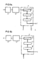
- Figur 8a und 8b zeigen eine Leitungsanschlußeinheit für niedrige Bitrate,FIGS. 8a and 8b show a line connection unit for low bit rate,
- Figur 9 zeigt ein erfindungsgemäßes Muldex mit einer DSO-Kanalverteilung,FIG. 9 shows a Muldex according to the invention with a DSO channel distribution,
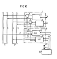
- Figur 10 zeigt das Prinzip einer Zusammenschaltung von mehr als vier erfindungsgemäßen Muldex undFIG. 10 shows the principle of an interconnection of more than four Muldex and
- Figur 11 zeigt einen Geräterahmen zur Aufnahme mehrerer erfindungsgemäßer Muldex.FIG. 11 shows a device frame for holding several Muldex according to the invention.
-
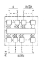
Figur 1 zeigt ein Blockschaltbild einer Anordnung 1 mit mehreren erfindungsgemäßen Muldex. Sie enthält mehrere Leitungsanschlußeinheiten 4 für niedrige Bitrate mit einem Anschluß 2, mehrere Leitungsanschlußeinheiten 5 für hohe Bitrate mit Anschluß 3 und ein Bussystem 6. Dieses ist mit allen Leitungsanschlußeinheiten 4 und 5 über Sendebus-Datenleitungen 7, Empfangsbus-Datenleitungen 8, Sendebus-Adressenleitungen 9 und Empfangsbus-Adressenleitungen 10 verbunden. An die Anschlüsse 2 können DSO-, DS1-, DS1C- oder DS2-Signale und an die Anschlüsse 3 können DS3-Signale angelegt oder an diesen entnommen werden.Figure 1 shows a block diagram of an
arrangement 1 with several Muldex according to the invention. It contains severalline connection units 4 for low bit rate with oneconnection 2, severalline connection units 5 for high bit rate with connection 3 and abus system 6. This is with allline connection units bus data lines 7, receivebus data lines 8, sendbus address lines 9 and receivebus address lines 10 connected. DSO, DS1, DS1C or DS2 signals can be connected toconnections 2 and DS3 signals can be applied to or taken from connections 3.
Bei Einsatz in der europäischen Digitalsignalhierarchie können beispielsweise an die Anschlüsse 2 2-Mbit/s-und/oder 8-Mbitls-Signale und an die Anschlüsse 3 34-Mbit/s-Signale angelegt werden.When used in the European digital signal hierarchy, 2 2 Mbit / s and / or 8 Mbitls signals can be applied to the connections and 3 34 Mbit / s signals can be applied to the connections.
Die Leitungsanschlußeinheiten 4 zerlegen ankommende Signale in 8-brt-Gruppen, die Datenbytes von einzelnen PCM-Kanälen sein können, und übertragen jede 8-bit-Gruppe zusammen mit einer Zieladresse (5) bzw. gesteuert von einer Zieladresse (4) an das Bussystem 6. Weil alle Leitungsanschlußeinheiten 4 und 5 mit dem Bussystem 6 verbunden sind und alle auf diesem ankommenden Signale überwachen, wird die gesendete 8-bit-Gruppe von der Leitungsanschlußeinheit empfangen und übernommen, die die Zieladresse verarbeitet. Diese fügt die 8-bit-Gruppe wiederum in einen geeigneten Zeitschlitz eines zu bildenden Digitalsignals ein. Die Adresse für jede 8-bit-Gruppe enthält sowohl eine Raum- als auch eine Zeitinformation, die von allen Leitungsanschlußeinheiten 4 und 5 verstanden wird, um diese 8-bit-Gruppe in den richtigen Anschluß 2 oder 3 und in den richtigen Zeitschlitz einzuspeisen.The
Im Vergleich mit dem relativ starren Durchschaltefeld und einzelnen fest verdrahteten Multiplexern nach dem Stand der Technik weist diese Erfindung sowohl eine flexiblere Verteil- als auch Muftiplexmöglichkeit auf.In comparison with the relatively rigid switching field and individual hard-wired multiplexers according to the state of the art, this invention has both a more flexible distribution and a multiplexing option.
Figur 2 zeigt die Anordnung nach Figur 1 mit einem detaillierter dargestellten Bussystem 6. Dieses enthält Sende-Busleitungen 11 und Empfangs-Busleitungen 12. Als Verbindungselemente zwischen den Leitungsanschlußeinherten 4 und 5 und dem Bussystem 6 sind Sendebus-Datenleitungen 7 und -Adressenleitungen 9 sowie Empfangsbus-Datenleitungen 8 und - Adressenleitungen 10 dargestellt. Der Anschluß 2 ist hier in einen Eingangsanschluß 2a und einen Ausgangsanschluß 2b aufgespaltet; entsprechend sind anstelle des Anschlusses 3 Eingangsanschlüsse 3a und Asgangsanschlüsse 3b gezeigt.FIG. 2 shows the arrangement according to FIG. 1 with a
Es gibt vier Sende-Busleitungen 11 und vier Empfangsbusleitungen 12, weil vier Leitungsanschlußeinheiten 5 für hohe Bitrate, also vier Muldex anzuschließen sind. Jede Sende-Busleitung 11 und jede Empfangs-Busleitung 12 umfaßt zwei Busleitungsbündel, eines für 8-bit-Gruppen und eines für Adresseninformationen.There are four transmit
Bei der Erläuterung der Figuren 6a und 6b wird nochmals auf die Figur 2 zurückgekommen.6a and 6b, reference is made again to FIG.
Die Figuren 3 und 4 zeigen die Busverbindungen zwischen einer Leitungsanschlußeinheit 4 für niedrige Bitrate und einer von vier Leitungsanschlußeinheiten 5 für hohe Bitrate. In Figur 3 werden vier DS1-Signale in ein DS3-Signal umgesetzt In Figur 4 ist die Rückumsetzung dargestellt.FIGS. 3 and 4 show the bus connections between a
Die Anordnung nach Figur 3 enthält die Eingangsanschlüsse 2a für niedrige Bitrate, Schnittstellen 13 für niedrige Bitrate, eine Decodier- und Überwachungsschaltung 14, Busanschalteeinrichtungen 15a bis 15d, Eingangsspeicher 16a und 16b, einen Parallel-Seriell-Umsetzer 17, einen DS3-Rahmenbildner 18, eine Schnittstelle 19 für hohe Bitrate, einen Ausgangsanschluß 3b, eine Buskontrollschaltung 20, Sendebus-Datenleitungen 7a bis 7d und Sendebus-Adressenleitungen 9a-9d.The arrangement according to FIG. 3 contains the
Die DS1-Signale gelangen über die Schnittstellen 13 und die Decodier- und Überwachungsschaltung 14 zu den Busanschafteeinrichtungen 15a - 15d. Von diesen reagiert jede auf eine Ursprungsadresse, die sie auf der zugehörigen Sendebus-Adressenleitung 9a, 9b, 9c oder 9d erhält, und liefert eine 8-bit-Gruppe - einen 8-bit-Abtastwert oder ein Datenbyte - an die ihr zugeordnete Sendebus-Datenleitung 7a, 7b, 7c oder 7d. Die Buskontrollschaftung 20, die die Adressen für eine Leitungsanschlußeinheit 5 für hohe Bitrate erzeugt, benennt auch einen der Eingangsspeicher 16a oder 16b für einen Empfang des Abtastwertes. Sowie dort Daten gesammelt werden, werden sie durch den Parallel-Seriell-Umsetzer und Multiplexer 17 verfügbar gemacht, was durch den DS3-Rahmenbildner 18 kontrolliert wird. Vom Parallel-Seriell-Umsetzer und Multiplexer 17 wird das Signal über die Schnittstelle 19 dem Ausgangsanschluß 3b zugeführt.The DS1 signals arrive via the
Die Anordnung nach Figur 4 enthält Ausgangsanschlüsse 2b, Schnittstellen 21 für niedrige Bitrate, einen Phasendiskriminator und Codierer 22, Busanschafteeinrichtungen 23a bis 23d, Busschnittstellen und Pufferschaltungen 24a und 24b, einen Seriell-Parallel-Umsetzer und Demultiplexer 25, eine Schnittstelle 26 für hohe Bitrate, einen Eingangsanschluß 3a, eine DS3-Synchronisierschaftung 27, eine Buskontrollschaltung 28, Empfangsbus-Datenleitungen 8a bis 8d und Empfangsbus-Adressenleitungen 10a bis 10d.The arrangement according to FIG. 4 contains
Ein am Eingangsanschluß 3a anliegendes DS3-Signal gelangt über die Schnittstelle 26 zum Seriell-Parallel-Umsetzer und Demultiplexer 25. Dieser liefert Signale an die DS3-Synchronisierschaftung 27, die den Parallel-Seriell-Umsetzer und Demultiplexer 25 auf den Rahmen des DS3-Signals synchronisiert. Die zeitlich durch die DS3-Synchronisierschaltung 27 eingestellte Buskontrollschaltung 28 steuert die Übertragung der 8-bit-Gruppen durch die Busschnittstellen und Pufferschaltungen 24a und 24b auf die Empfangsbus-Datenleitungen 8a bis 8d. Gleichzeitig liefert die Buskontrollschaltung 28 an die Busanschalteeinrichtungen 23a bis 23d eine Zieladresse für die Leitungsanschlußeinheiten 4. Durch diese wird bewirkt, daß die jeweilige 8-bit-Gruppe den passenden DS1-Ausgangsanschluß 2b erreicht. Dabei passiert die 8-bit-Gruppe den Phasendiskriminator und Codierer 22 und eine Schnittstelle 21.A DS3 signal present at the
Figur 5 ist ein Blockdiagramm, das darstellt, wie eine Leitungseinheit 4 für niedrige Bitrate und eine Leitungsanschlußeinheit 5 für hohe Bitrate über das Bussystem 6 verbunden sind. Wie bereits erwähnt, gibt es vier getrennte Sende-Busleitungen 11, von denen jede Sendebus-Datenleitungen 7 und Sendebus-Adressenleitungen 9 enthält, und vier getrennte Empfangs-Busleitungen 12. von denen jede Empfangsbus-Datenieitungen 8 und Empfangsbus-Adressenleitungen 10 umfaßt. Jede Leitungsanschlußeinheit 5 ist an eine Sende-Busleitung 11 und eine Empfangs-Busleitung 12 angeschlossen. Jede Leitungsanschlußeinheit 4 ist andererseits an alle Sende-Busteitungen 11 und an alle Empfangs-Busleitungen 12 angeschlossen. Empfangene 8-bit-Gruppen eines DS1-Signals werden in den Pufferspeicher 29 eingespeist, von denen aus sie zu bestimmten Zeiten an die Sendebus-Datenleitungen 7 abgegeben werden, nachdem sie durch vom Adressen-Decoder 30 empfangene Zieladressen ausgewählt wurden. Ähnlich werden von der Leitungsanschlußeinheit 5 empfangene 8-bit-Gruppen in Pufferspeicher 31 der Leitungsanschlußeinheit 4 in Reaktion auf die von den Adressen-Decodern 32 empfangenen Zieladressen eingegeben.FIG. 5 is a block diagram illustrating how a
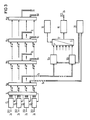
Die Figuren 6 und 7 zeigen die Wirkungsweise der Leitungsanschlußeinheiten 5. Die Figur 6a zeigt, wie 8-bit-Gruppen von der Sendebus-Datenleitung 7 zum Ausgangsanschluß 3b laufen. Figur 6b zeigt, wie 8-bit-Gruppen vom Eingangsanschluß 3a zur Empfangsbus-Datenleitung 8 gelangen.FIGS. 6 and 7 show the mode of operation of the
Die Anordnung nach Figur 6a enthält einen Codeumsetzer 35, Zusatzspeicher 37a und 37b, achtundzwanzig Eingangsspeicher 38, einen Zähler 40, einen Kanalzuordnungsspeicher 42 und den Multiplexer und Parallel-Seriell-Umsetzer 17 mit Ausgangsanschluß 3b. Auf der Sendebus-Datenleitung 7 eintreffende 8-bit-Gruppen werden in Eingangsspeicher 38 aufeinanderfolgend eingespeist Die Auswahl des jeweiligen Eingangsspeichers 38 erfolgt über einen ersten Ausgang 39 des Zählers 40. Eine der 8-bit-Gruppen wird nicht in einen der Eingangsspeicher 38, sondern in den Zusatzspeicher 37a eingegeben. Der Zähler 40 wählt so aufeinanderfolgend einen von achtundzwanzig DS1-Eingangsanschlüssen 2a für abgehende Übertragung zu dem DS3-Ausgangsanschluß 3b. Der neunundzwanzigste Zeitschlitz ermöglicht eine Verteilung, eine Überwachung sowie ein Abzweigen von 8-bit-Gruppen mittels des Zusatzspeichers 37a. Der Zähler 40 betätigt den Zusatzspeicher 37a für die Übertragung von 8-bit-Gruppen in diesen Zeitschlitz.The arrangement of Figure 6a includes a
Im DSO-Betrieb enthält jede 8-bit-Gruppe ein Datenbyte eines 24-Kanal-PCM-Signals. Der Zähler 40 ist jetzt um einen (1 bis 24)-Zähler erweitert, der nach jedem Durchlauf des (1 bis 29)-Zählers weiterzählt.In DSO mode, each 8-bit group contains a data byte of a 24-channel PCM signal. The counter 40 is now extended by a (1 to 24) counter which continues to count after each passage through the (1 to 29) counter.
Der zweite Ausgang 41 des Zählers 40 adressiert den Kanalzuordnungsspeicher 42 in dem 12-bit-Zieladressen auf neunundzwanzig Plätzen für DS1-Betrieb oder auf sechshundertsechsundneunzig Plätzen für DSO-Betrieb gespeichert sind. Nach Adressierung speist der Kanalzuordnungsspeicher 42 die ausgewählte Zieladresse in die Sendebus-Adressenleitung 9 ein.The
Die 8-bit-Gruppen auf jeder Sendebus-Datenleitung 7 und jeder Empfangsbus-Datenleitung 8 - wie sie bereits in Figur 2 vorgestellt wurden - erfordern acht parallele Drähte. Jede 12-bit-Zieladresse wird für eine Übertragung vom Kanalzuordnungsspeicher 42 über die Sendebus-Adressenleitung 9 durch den Codeumsetzer 35 aufbereitet. in den Adressenleitungen 9 und 10 ist je eine von sechszehn Leitungen für eine Auswahl einer von sechzehn Leitungsanschlußeinheiten 4 vorgesehen. Drei weitere Leitungen identifizieren eine von acht Anschlüssen 2. Jede Leitungsanschlußeinheit 5 kann dann einen aus bis zu einhundertachtundzwanzig möglichen DS1-Plätzen adressieren.The 8-bit groups on each send
Bei Übertragung der zugehörigen Zieladressen auf einer der Sendebus-Adressenleitungen 9 sind 8-bit-Gruppen eines bestimmten DS1-Signals (eines aus acht) der adressierten Leitungsanschlußeinheit 4 (einer aus sechzehn) an die Sendebus-Datenleitung 7 angelegt. Beim Senden der bestimmten Zieladresse auf einer der vier Sendebus-Adressenleitungen 9a bis 9d aktiviert in dem infragekommenden Zeitschlitz die Leitungsanschlußeinheit 5 die Übertragung der Zieladressen über die zugeordnete Sendebus-Datenleitung 7a, 7b, 7c oder 7d zu dem bestimmten Eingangsspeicher 38 der Leitungsanschlußeinheit 5.When the associated destination addresses are transmitted on one of the send
Die Reihenfolge der Übertragung über das Bussystem 6 wird durch Einschreiben von Zieladressen in den Kanalzuordnungsspeicher 42 gesteuert. Die Inhalte von dessen Speicherplätzen werden regelmäßig für die Zeitdauer eines Zeitschlitzes über den Codeumsetzer 35 an die Sendebus-Adressenleitung 9 angelegt. So wird für jeden Zeitschlitz .festgelegt, welche 8-bit-Gruppe von einer Leitungsanschlußeinheit 4 über die zugeordnete Sendebus-Datenleitung 7a, 7b, 7c oder 7d übertragen wird. Weil diese Sendebus-Datenleitung ständig einer bestimmten Lertungsanschlußeinheit 5 zugeteilt ist, bestimmen die Zieladressen in den Speicherplätzen die Ziel-Leitungsanschlußeinheit 5 und den Ausgangsanschluß 3b. Jede Sendebus-Datenleitung 7a bis 7d überträgt zeitverschachtelt wenigstens achtundzwanzig und vorzugsweise neunundzwanzig DS1-Signale. Die Taktfrequenz des Bussystems 6 muß infolgedessen wenigstens 1,544 MHz x 29 = 45 MHz betragen. Weil jedoch eine 8-bit-Gruppe über acht Leitungen parallel übertragen wird, beträgt die Taktfrequenz des Bussystems 6 nur etwa 6 MHz.The order of transmission via the
Ein DS1C-Signal wird in zwei DS1-Signale aufgeteilt und anschließend in der oben beschriebenen Art durchverbunden.A DS1C signal is divided into two DS1 signals and then connected through in the manner described above.
Die Anordnung in Figur 6b enthält einen Parallel-Seriell-Umsetzer und Demultiplexer 25 mit Eingangsanschluß 3a, achtundzwanzig Ausgangsspeicher 43, einen Zähler 44, einen Kanalzuordnungsspeicher 45, einen Zusatzspeicher 37b und einen Codeumsetzer 36.The arrangement in FIG. 6b contains a parallel-serial converter and
Ein an den Eingangsanschluß 3a angelegtes DS3-Signal wird im Parallel-Seriell-Umsetzer und Demultiplexer 25 zerlegt und den Ausgangsspeichern 43 zugeführt. Diese werden durch den Zähler 44 ausgewählt. Eine 8-bit-Gruppe wird nicht in einen der Ausgangsspeicher 43 sondern in den Zusatzspeicher 37b eingegeben. Der Zähler 44 wählt so aufeinanderfolgend einen von achtundzwanzig DS1-Ausgangsanschlüssen 2b für abgehende Übertragung. Bei DSO-Betrieb wählt der Zähler 44 dagegen aufeinanderfolgend einen von vierundzwanzig DSO-Kanälen. Die Ausgangsspeicher 43 speisen die Empfangsbus-Datenleitung 8 und der Kanalzuordnungsspeicher 45 die Empfangsbus-Adressenleitung 10.A DS3 signal applied to the
Figur 7 zeigt deutlicher als Figur 6a, wie jeder DS3-Rahmen durch den Parallel-Seriell-Umsetzer und Multipexer 17 erzeugt wird. Dieser empfängt 8-bit-Gruppen der Eingangsspeicher 38 und fügt hintereinander die einzelnen Bits der 8-bit-Gruppen. gesteuert durch die DS3-Rahmensynchronisierschaltung 46 in einen DS3-Rahmen. Jeder der Eingangsspeicher 38 besteht aus zwei Abschnitten: Einer Eingangskippstufe 47 (latch), die durch ein Signal von einem Decoder 49 aktiviert wird, und einer Ausgangskippstufe 48 (latch). Er verhält sich wie ein Pufferspeicher, wie er in konventionellen Multiplexern Verwendung findet.FIG. 7 shows more clearly than FIG. 6a how each DS3 frame is generated by the parallel-serial converter and
Der Teil der Leitungsanschlußeinheiten 4, welcher für die ankommenden DS3-Signale gemäß Figur 6b zuständig ist, ist im Prinzip identisch und arbeitet in umgekehrter Weise auf den abgehenden gerade beschriebenen Teil.The part of the
Die Figuren 8a und 8b zeigen die Arbeitsweise einer Leitungsanschlußeinheit 4.FIGS. 8a and 8b show the mode of operation of a
Wie Figur 8a zeigt, empfängt die Leitungsanschlußeinheit 4 mit Hilfe der Sendebus-Adressenleitung 9 eine Zieladresse. Diese veranlaßt die Leitungsanschlußeinheit 4, eine 8-bit-Gruppe auf die Sendebus-Datenleitung 7 zu geben. Diese 8-bit-Gruppe ist eine parallele Darstellung der seriellen DS1-Daten, die in die Leitungsanschlußeinheit 4 durch die Schnittstelle 13 gelangen. Im DSO-Betrieb identifiziert ein DS1-Demultiplexer 50 die einzelnen DSO-Bytes (8 bit) im DS1-Signal. Da der Leitungsanschlußeinheit 5 öfters eine Zieladresse präsentiert wird als DSO-Bytes von der Leitungsanschlußeinheit 4 verfügbar sind, muß eine "Pufferspeicher-Leer"-Anzeige L die Leitungsanschlußeinheit 5 über die Gültigkeit der Daten auf der Sendebus-Datenleitung 7 auf dem laufenden halten.As FIG. 8 a shows, the
Wie Figur 8b zeigt, ist die Struktur der Leitungsanschlußeinheit 4 in Empfangsrichtung komplementär. Die Leitungsanschlußeinheit 4 enthält einen Parallel-Seriellumsetzer 56, Pufferspeicher 57 und 58, im DSO-Betrieb zusätzlich einen Muftiplexer 55 und eine Schnittstelle 19.As FIG. 8b shows, the structure of the
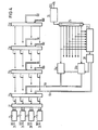
Figur 9 zeigt ein erfindungsgemäßes Muldex mit einer Leitungsanschlußeinheit 4 für niedrige Bitrate, mit einem Bussystem 6 für DSO-Betrieb und mit einer Leitungsanschlußeinheit 5 für hohe Bitrate.FIG. 9 shows a Muldex according to the invention with a
Die Leitungsanschlußeinheit 4 enthält in Senderichtung acht DS1-Demultiplexer und Seriell-Parallel-Umsetzer 65, von denen nur einer gezeigt ist, einen adressierbaren Schreib-Lese-Speicher 59, eine Datenbus-Schnittstelle oder Datenbus-Treiber 61 sowie einen Adressenbus-Empfänger 63 und in Empfangsrichtung einen Datenbus-Empfänger 62, einen Adressenbus-Empfänger 64, einen adressierbaren Schreib-Lese-Speicher 60, eine logische Schaltung 67 und acht DS1 -Muitipiexer und Parallel-Seriell-Umsetzer 66, von denen nur einer gezeigt ist.The
Die Leitungsanschlußeinheit 5 enthält einen Parallel-Seriell-Umsetzer und Multiplexer 17, Eingangsspeicher 38, adressierbare Schreib-Lese-Speicher 73 und 74, einen Busempfänger 69, Bustreiber 70 bis 72, Kanalzuordnungsspeicher 42 und 45, Seriell-Parallel-Umsetzer und Demuitiplexer 25 und Ausgangsspeicher 43. Die Eingangsspeicher 38 und die Ausgangsspeicher 43 vermögen sechshundertzweiundsiebzig DSO-Kanal-Datenwerte zu speichern.The
Die Leitungsanschlußeinheit 4 wurde bereits anhand der Figuren 8a und 8b und die Leitungsanschlußeinheit 5 anhand der Figuren 6a und 6b näher erläutert. In Klammern gesetzte Zahlen geben die Anzahl paralleler Drähte an. Die Leitungsanschlußeinheit 4 enthält in den adressierbaren Schreib-Lese-Speicher 59 zusätzlich zum bereits empfohlenen Pufferspeicher mit ausreichender elastischer Speicherkapazität zum Speichern von Abtastwerten aus allen gedemultiplexten DSO-Kanälen von allen acht DS1-Demultiplexem und Seriell-Parallel-Umsetzern 65 oder sonstigen DSO-Anschlüssen.The
Zur Erläuterung der Prinzipien der vorliegenden Erfindung werden nachfolgend einzelne hypothetische Situationen diskutiert. Zuerst wird die Selektion eines DSO-Kanals in einer Leitungsanschlußeinheit 4 besprochen. Diese ist derart gestaltet, daß der selektierte DSO-Kanal durchgeschaltet und in einen bestimmten Zeitschlitz am Ausgangsanschluß 3b gemultiplext wird.To explain the principles of the present invention, individual hypothetical situations are discussed below. First, the selection of a DSO channel in a
Anschließend wird der DSO-Kanal-Empfang diskutiert, der zu einem abgehenden DSO-Kanal in demselben DS1-Signal oder einem anderen DS1-Signal rückübertragen wird. Es wird dabei angenommen, daß die gezeigte DS1-Multiplexer/Demultiplexer-Kombination derselben DS1-Leitung zugeordnet ist.Then the DSO channel reception is discussed, which is retransmitted to an outgoing DSO channel in the same DS1 signal or another DS1 signal. It is assumed that the DS1 multiplexer / demultiplexer combination shown is assigned to the same DS1 line.
In dem DSO/DS3-Beispiel hat in der Senderichtung die Leitungsanschlußeinheit 5 in ihrem Kanalzuordnungsspeicher 42 eine Adresse gespeichert, die einem bestimmten DSO-Kanal (beispielsweise einem von vierundzwanzig) in einem bestimmten DS1-Signal in der Leitungsanschlußeinheit 4 zugeordnet ist Ferner ist die Leitungsanschlußeinheit 5 vorprogrammiert, um Daten von den Eingangsspeichem 38 derart zu übergeben, daß der in einem bestimmten Zeitschlitz des Bussystems 6 adressierte DSO-Kanal in bestimmte Zeitschlitze des DS3-Signals am Ausgangsanschluß 3b eingefügt wird.In the DSO / DS3 example, in the transmission direction, the
Während der in Figur 6a gezeigte Zähler 40 durch die Kanäle und damit durch die des DS3-Signais zugeordneten Zieladressen läuft, zählt er schließlich bis zu der Zieladresse im Kanalzuordnungsspeicher 42 von dem betrachteten DSO-Kanal des betrachten DS1-Signals. Die 12-bit-Zieladresse wird im wesentlichen zur Sendebus-Adressenleitung 9 über den Bustreiber 70 gegeben. Während sie zu allen Leitungsanschlußeinheiten 4 gesendet wird, läßt lediglich eine vorgewählte Leitungsanschlußeinheit 4 die übertragene Adresse zum Adressenbusempfänger 63 durch. Dazu wählen 4 bit eine von sechzehn Lertungsanschlußeinheiten 4, was mit Hilfe einer nicht gezeigten Baugruppen-Auswahlleitung durchgeführt wird. Ein bestimmtes DS1-Signal wird aus acht DS1 Signalen (von vierundzwanzig DSO-Kanälen) durch weitere 3 bit einer Information identifiziert Weitere 5 bit werden verwendet, um einen DSO-Kanal aus einem bestimmten DS1-Signal auszuwählen.While the counter 40 shown in FIG. 6a runs through the channels and thus through the target addresses assigned to the DS3 signal, it finally counts up to the target address in the
Der DS1-Demultiplexer in 65 zerlegt kontinuierlich einen seriellen Datenstrom in seine vierundzwanzig DSO-Datenbytes. Der Seriell-Parallel-Umsetzer in 65 übernimmt dann deren Umsetzung in parallele DSO-Datenbytes und fügt ein Paritätsbit und ein Stopfbit hinzu. Die vierundzwanzig DSO-Datenbytes mit den Paritätsbits und Stopfbits werden in aufeinanderfolgenden Adressenplätzen im adressierbaren Schreib-Lese-Speicher 64 gespeichert.The DS1 demultiplexer at 65 continuously breaks down a serial data stream into its twenty-four DSO data bytes. The serial-to-parallel converter in 65 then converts them into parallel DSO data bytes and adds a parity bit and a stuff bit. The twenty-four DSO data bytes with the parity bits and stuff bits are stored in successive address locations in the addressable read-write memory 64.
Zur selben Zeit, während der der serielle Datenstrom zerlegt wird, werden vier Markierungsbits Sa,Sb,Sc und 5d, die den sechsten, zwölften, achtzehnten und vierundzwanzigsten Rahmen des DS1-Signals anzeigen, zum adressierbaren Schreib-Lese-Speicher 64 für eine erweiterte Überrahmenbildung (extended frame) übertragen. Insgesamt kann die parallele Datenübertragung für einen bestimmten DSO-Kanal 14 bit enthalten: 8 bit repräsentieren ein DSO-Datenbyte, 4 bit Markierungsbits Sa, Sb, Sc und Sd für den erweiterten Überrahmenbetrieb, 1 bit ein Paritätsbit und 1 bit ein Stopfbit.At the same time that the serial data stream is being decomposed, four marker bits Sa, Sb, Sc and 5d, which indicate the sixth, twelfth, eighteenth and twenty-fourth frames of the DS1 signal, become the addressable read-write memory 64 for an expanded one Transfer extended frame. Overall, the parallel data transmission for a particular DSO channel can contain 14 bits: 8 bits represent a DSO data byte, 4 bit marking bits Sa, Sb, Sc and Sd for extended superframe operation, 1 bit a parity bit and 1 bit a stuff bit.
Bei Adressierung über die Sendebus-Adressenleitung 9 sendet ein bestimmter Speicherplatz für DSO-Signale die 14 bit parallel zur Busschnittstelle oder Datenbustreiber 61.When addressing via the send
Der Datenbustreiber 61 gibt während eines Zeitschlitzes des Bussystems 6 14-bit-Daten ab, die vom Bussystem 6 übertragen werden. Diese Daten werden während des obengenannten Zeitschlitzes vom Busempfänger 69 der Sendebus-Datenleitung 7 erwartet. Wenn der Busempfänger 69 diese 14 bit parallel empfängt, werden die 10 bit der Daten einschließlich des Paritätsbits und des Stopfbits durch die Eingangsspeicher 38 parallel zum Parallel-Seriell-Umsetzer in 17 und seriell zum Multiplexer in 17 geliefert. A-, B-, C-und D-Signalisierungsbits (vermittlungstechnische Kennzeichen) in den durch die Markierungsbits Sa, Sb, Sc und Sd markierten DSO-Bytes werden extrahiert und in den adressierbaren Schreib-Lese-Speicher 73 für eine zeitweilige Speicherung zur Ausgabe in den sechsten, zwölften, achtzehnten und vierundzwanzigsten Rahmen der seriellen Datenübertragung geliefert.During a time slot of the
In Empfangsrichtung am Eingangsanschluß 3a empfangene serielle Daten eines DS3-Signals werden vom Demultiplexer in 25 empfangen. Der Seriell-Parallel-Umsetzer in 25 extrahiert die DSO-Datenbytes und liefert diese sowie das Paritätsbit und das Stopfbit über die Ausgangsspeicher 43 zum Bustreiber 72. Die A-, B-, C-und D-Signalisierungsbits der sechsten, zwölften, achzehnten und vierundzwanzigsten Rahmen werden zu einem A-, B-, C-und D-Speicherplatz im adressierbaren Schreib-Lese-Speicher 74 zur zeitweiligen Speicherung geliefert. Der Bustreiber 72 liefert das kombinierte 14-bit-Signai parallel zur Empfangsbus-Datenleitung 8. Eine 12-bit-Zieladresse wird vom Kanalzuordnungsspeicher 45 über den Bustreiber 71 auf die Empfangsbus-Adressenleitung 10 und auf die bereits erwähnte individuelle Baugruppen-Auswahlleitung gleichzeitig mit den vierzehn Datenbits gesendet, die durch den Adressenbus-Empfänger 64 und den Datenbus-Empfänger 62 empfangen werden. Die Zieladressendaten identifizieren genau, für welchen DSO-Kanal der DS1 -Leitung die Daten bestimmt sind. Diese werden in den individuell adressierten Speicherplatz des adressierbaren Schreib-Lese-Speichers 69 geladen.Serial data of a DS3 signal received in the receiving direction at the
Der adressierbare Schreib-Lese-Speicher 60 gibt die zehn Datenbits und die A-, B-, C- und D-Signalisierungsbits parallel ab, wenn ein nicht gezeigter kontinuierlich fortlaufender Zähler in der Leitungsanschlußeinheit 4 diese Adresse erreicht. Sie werden zuerst zur Logikschaftung 67 geleitet, deren Betrieb durch den DS1-Multiplexer in 66 kontrolliert wird. Dieser signalisiert der Logikschaltung 67, wenn die A-, B-, C- und D-Signalisierungsbits in den sechsten, zwölften, achzehnten und vierundzwanzigsten Rahmen am Eingang des Parallel-Seriell-Umsetzers in 66 einzufügen sind. Zuletzt wird der DSO-Datenwert in den vorausgewählten einen von vierundzwanzig DSO-Kanalausgängen des DS1-Multiplexers in 66 geliefert.The addressable read-
So wurde ein Mittel zum Anschließen von beispielsweise DSO-Kanal Nr. 8 aus vierundzwanzig Kanäien in einem einzelnen DS1-Signal dargestellt. Daten dieses Kanals sind im dargestellten Beispiel durchgeschaltet und gemultiplext, beispielsweise zum DSO-Kanal Nr. 97 aus sechshundertzweiundsiebzig Kanälen eines einzelnen DS3-signals.For example, a means of connecting, for example,
Jetzt wird die Durchschaltung in der DSO-Ebene für den Fall beschrieben, daß die Durchschaltung in demselben oder einem anderen DS1-Signal bewirkt wird. Zum Beispiel kann der Kanal Nr. 8 aus vierundzwanzig Kanälen in einem DS1-Signal mit dem Kanal Nr. 3 aus vierundzwanzig Kanälen desselben oder eines anderen DS1-Signals verbunden werden. Es ist wichtig zu erkennen, daß eine Kontrolle des Prozesses Über eine Leitungsanschlußeinheit 5 erfolgt. Die Kanäle in der Richtung von Kanal Nr. 3 zum Kanal Nr. 8 und umgekehrt werden durch 12-bit-Zieladressen kontrolliert, die durch die Leitungsanschlußeinheit 5 ausgesendet werden.The switching in the DSO level in the event that the switching is effected in the same or a different DS1 signal will now be described. For example,
Für eine Übertragung zwischen verschiedenen DS1-Signalen werden die Daten über die Sendebus-Datenleitung 7 zur Leitungsanschlußeinheit 5 übertragen, in dem Zusatzspeichern 37a in den Figuren 6a und 6b gespeichert und zur Leitungsanschlußheit 4 in insgesamt zwei Adressen-/Datenübertragungszyklen zurückübertragen.For a transmission between different DS1 signals, the data are transmitted via the transmission
In dem Muldex nach Figur 9 können unter der Kontrolle der Leitungsanschlußeinheit 5 in Übereinstimmung mit der vorangegangenen Diskussion folgende besondere Funktionen ausgeführt werden: Eine sogenannte Überwachungsfunktion, eine sogenannte Verteilfunktion und eine sogenannte Abzweigfunktion.The following special functions can be carried out in the Muldex according to FIG. 9 under the control of the
In der Überwachungsfunktion ist insbesondere einer der neunundzwanzig DS1-Sende- und Empfangsbuszeitschlitze auf entweder der Sendebus-Datenleitung 7 oder der Empfangsbus-Datenleitung 8 zu einer vorbestimmten Leitungsanschlußeinheit 4 für Überwachung, Test oder andere Zwecke leitbar.In the monitoring function, in particular one of the twenty-nine DS1 transmission and reception bus time slots on either the transmission
In der Verteilfunktion kann ein von irgendeiner Leitungsanschlußeinheit 4 kommendes Signal in irgendeinen der neunundzwanzig DS1-Zeitschlitze eingesetzt werden.In the distribution function, a signal coming from any
In der Abzweigfunktion können DS1-Daten von einem Seriell-Parallel-Umsetzer in 25 direkt zu dem Parallel-Seriell-Umsetzer in 17 umgeleitet werden.In the branch function, DS1 data can be redirected from a serial-to-parallel converter in 2 5 directly to the parallel-to-serial converter in FIG. 17.
Die Folge der gesamten Datenübertragung ist durch die in den Kanalzuordnungsspeichem 42 und 45 eingespeicherten Zieladressen bestimmt.The sequence of the entire data transmission is determined by the destination addresses stored in the
Mit Bezug auf die Figuren 10 und 11 wird weiter vorgeschlagen, die vorliegende Erfindung in Einschübe zu unterteilen. Jede einzelne Komponente, jeder Baustein oder jede Baueinheit kann mittels CMOS-Technologie ausgeführt werden. Beispielsweise kann eine Leitungsanschlußeinheit 4 für niedrige Bitrate ohne DSO-Betrieb aus lediglich zwei integrierten Schaltungschips für jedes DS1-Signal aufgebaut werden: einer für Parallel-Seriell- und Seriell-Parallel-Umsetzung, der andere für Coder- /Decoder-Funktionen und die Überwachung. Die Leitungsanschlußeinheit 5 für hohe Bitrate kann aus zwei fundamentaleren Bausteinchips bestehen, während eine Baugruppe niederer Bitrate bei DSO-Betrieb eine abweichende Gestaltung erfordert, aber aus einem ähnlichen Paar von Bausteinchips aufgebaut werden kann.With reference to FIGS. 10 and 11, it is further proposed to divide the present invention into inserts. Every single component, every component or every unit can be implemented using CMOS technology. For example, a
Figur 11 zeigt einen Geräterahmen 86 für die Aufnahme mehrerer erfindungsgemäßer Muldex. Im Geräterahmen 86 sind eine Betriebsstromversorgung 87, eine Reservestromversorgung 88, den Anschlüssen 2 und 3 vorgeschaltete Schutzrelais 92 und eine Leiterplatte an der Rückseite des Geräterahmens 86 eingebaut. Weiter enthält der Geräterahmen 86 Einschubfassungen, in die Einschübe einführbar sind, die über Steckverbindungen Kontakt zur Leiterplatte haben, auf der unter anderem das Bussystem 6 angeordnet ist. In die Einschubfassungen werden zuerst die zu einem Muldex gehörenden Einschübe 90 mit Leitungsanschiußeinheiten 4, Einschübe 89 mit Leitungsanschlußeinheiten 5 und Meßeinschübe 91 eingesteckt. In die noch freien Einschubfassungen können jeweils assoziiert mit einem Einschub 89 Buserweiterungs-Baugruppe 85 eingesteckt werden.FIG. 11 shows a
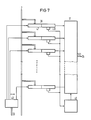
Figur 10 zeigt, daß für eine Zusammenarbeit von mehr als vier Muldex zu jeder Leitungsanschlußeinheit 5 eine Buserweiterungs-Baugruppe 85 gebraucht wird. Diese enthält einen DS3-Sender-Erweiterungsteil 80 in Form eines adressierbaren Schreib-Lese-Speichers und einen DS3-Empfänger-Erweiterungsteil 82 ebenfalls in Form eines adressierbaren Schreib-Lese-Speichers, um eine Speicherung von Daten für zwei Übertragungsrichtungen einer Leitungsanschlußeinheit 5 zu ermöglichen. Jeder dieser adressierbaren Schreib-Lese-Speicher 80 und 82 dient zur Speicherung von sechshundertzweiundsiebzig DSO-Kanal-Datenwerten für jede Übertragungsrichtung. Ferner ist die Buserweiterungs-Baugruppe 85 durch die gezeigte Leitungsanschlußeinheit 5 direkt adressierbar. Die Buserweiterungs-Baugruppe 85 erweitert außerdem das Bussystem 6 zu anderen Muldex entweder über die Busmatrix-Kontrolleinrichtung 84 oder mit Hilfe direkter Verbindungen. Die Leiter 81 und 83 können für eine Komplettierung der Verbindungen gebraucht werden. Auf diese Weise kann die Kapazität des beschriebenen Systems sehr erweitert und können seine Eigenschaften gesteigert werden. Im einzelnen umfaßt die Buserweiterungs-Baugruppe 85 einen Anschluß 77 zum Bussystem 6, Anschlüssen 78 zu einem Sender 75 und einen Empfänger 76 in der Leitungsanschlußeinheit 5 sowie Kontrolleitungsanschlüsse 79 von der kontrollierenden Leitungsanschlußeinheit 5.FIG. 10 shows that a
In Figur 11 sind vier Buserweiterungs-Baugruppen 85 gezeigt, welche die vier Einschübe 89 mit Leitungsanschlußeinheiten 5 oder drei Einschübe 89 und einen Reserveeinschub 89 ergänzen.In Figure 1 1 four
Gemäß Figur 10- werden - bei normalerweise nicht erweitertem Überrahmenbetrieb - Daten von der Sendebus-Datenleitung 7 durch einen Sender 76 zum DS3-Sendeteil 33 und empfangene DS3-Daten über den Empfänger 76 zur Empfangsbus-Datenleitung 8 geleitet. Der Sender 75 bzw. der Empfänger 76 sind Zusammenfassungen der vorher im Detail beschriebenen Busannahme-, Datenspeicherungs-, Zähl- usw. Funktionen.According to FIG. 10, data is transmitted from the transmission
Im erweiterten Busbetrieb für mehr als vier Leitungsanschlußeinheiten 5 werden in der Senderichtung Daten von einer Leitungsanschlußeinheit 4 über die Sendebus-Datenleitung 7 in den adressierbaren Schreib-Lese-Speicher 80 eingeführt; in analoger Weise wie sie bei normalem Betrieb in die Leitungsanschlußeinheit 5 eingeführt werden. Die der Buserweiterungs-Baugruppe 85 zugeordnete Leitungsanschlußeinheit 5 wird dabei nicht tangiert, da das Ziel der Daten ein anderer Muldex ist. Die Busmatrix-Kontrolleinrichtung 84 überträgt die Daten zu dieser Einrichtung. Wenn Daten aus einem anderen Muldex für einen Ausgang der Leitungsanschlußeinheit 5 bestimmt sind, werden die Daten durch den DS3-Sende-Erweiterungsteil 80 über eine direkte Verbindung zum Sender 75 und zum DS3-Sendeteil 33 geleitet.In extended bus operation for more than four
Im erweiterten Busbetrieb können die im DS3-Empfangsteil 34 empfangenen Daten, die normalerweise durch den Empfänger 76 zur Empfangsbus-Datenleitung 8 durchgeschaltet werden, jetzt durch eine direkte Verbindung zum DS3-Empfänger-Erweiterungsteil 82 und anschließend zur Busmatrix-Kontrolleinrichtung 84 weitergegeben werden. Im DS3-Empfänger-Erweiterungsteil 82 über die Leitung 83 empfangene Daten werden zur Empfangsbus-Datenleitung 8 ausgegeben. Eine Leitungsanschiußeinheil 4 vermag keinen Unterschied zwischen diesen Daten und den vom Empfänger 76 festzustellen.In the extended bus mode, the data received in the DS3 receiving part 34, which are normally switched through by the
Claims (8)
dadurch gekennzeichnet,
daß Sendebus-Datenleitungen (7,7a,7b), Empfangsbus-Datenleitungen (8,8a-8d), Sendebus-Adressenleitungen (9,9a-9d), Empfangsbus-Adressenleitungen (10,10a-10d) und Busanschlußeinrichtungen (15a-15d,23a-23d) mit Speicher (16a,16b,24a,24b,52,53,57,58) und Speichersteuerung in Form eines Adressenbusempfängers (63,64) vorgesehen sind.2. Muldex according to claim 1,
characterized,
that transmission bus data lines (7,7a, 7b), reception bus data lines (8,8a-8d), transmission bus address lines (9,9a-9d), reception bus address lines (10,10a-10d) and bus connection devices (15a-15d , 23a-23d) with memory (16a, 16b, 24a, 24b, 52, 53, 57, 58) and memory control in the form of an address bus receiver (63, 64) are provided.
dadurch gekennzeichnet,
characterized,
dadurch gekennzeichnet,
daß im ersten adressierbaren Schreib-Lese-Speicher (52,53,59) eine bestimmte Adresse wenigstens ein bestimmtes Byte aus einem bestimmten Zeitkanal enthält und daß im zweiten adressierbaren Schreib-Lese-Speicher (57,58,60) ein bestimmtes Byte für eine Übertragung zu einem bestimmten Zeitkanal gemäß der Adressensignalisierung bereitgestellt wird.4. Muldex according to claim 3,
characterized,
that in the first addressable read-write memory (52,53,59) a certain address contains at least a certain byte from a certain time channel and that in the second addressable read-write memory (57,58,60) a certain byte for one Transmission to a specific time channel is provided according to the address signaling.
dadurch gekennzeichnet,
characterized,
dadurch gekennzeichnet,
daß in der zweiten Busanschlußeinrichtung (23a-23d) zwichen dem zweiten adressierbaren Schreib-Lese-Speicher (60) und dem Multiplexer und Parallel-Seriell-Umsetzer (66) eine logische Schaltung (67) vorgesehen ist, die einem rahmensynchronen Einsetzen von Signalisierungsbits in den Datenstrom dient.6. Muldex according to one of claims 3 to 5,
characterized,
that a logic circuit (67) is provided in the second bus connection device (23a-23d) between the second addressable read-write memory (60) and the multiplexer and parallel-serial converter (66), which enables frame-synchronous insertion of signaling bits in serves the data stream.
dadurch gekennzeichnet,
characterized,
dadurch gekennzeichnet,
characterized,
Priority Applications (1)
| Application Number | Priority Date | Filing Date | Title |
|---|---|---|---|
| AT85116257T ATE67361T1 (en) | 1984-12-20 | 1985-12-19 | MULDEX WITH CHANNEL DISTRIBUTOR FOR DIGITAL SIGNALS OF DIFFERENT HIERARCHY LEVELS. |
Applications Claiming Priority (4)
| Application Number | Priority Date | Filing Date | Title |
|---|---|---|---|
| US683901 | 1984-12-20 | ||
| US06/683,901 US4685101A (en) | 1984-12-20 | 1984-12-20 | Digital multiplexer for PCM voice channels having a cross-connect capability |
| US06/758,990 US4697262A (en) | 1984-12-20 | 1985-07-25 | Digital carrier channel bus interface module for a multiplexer having a cross-connect bus system |
| US758990 | 1985-07-25 |
Publications (3)
| Publication Number | Publication Date |
|---|---|
| EP0186141A2 true EP0186141A2 (en) | 1986-07-02 |
| EP0186141A3 EP0186141A3 (en) | 1988-08-17 |
| EP0186141B1 EP0186141B1 (en) | 1991-09-11 |
Family
ID=27103222
Family Applications (1)
| Application Number | Title | Priority Date | Filing Date |
|---|---|---|---|
| EP85116257A Expired - Lifetime EP0186141B1 (en) | 1984-12-20 | 1985-12-19 | Multiplexer demultiplexer with a channel distributor for digital signals of different hierarchical levels |
Country Status (7)
| Country | Link |
|---|---|
| US (1) | US4697262A (en) |
| EP (1) | EP0186141B1 (en) |
| AU (1) | AU579543B2 (en) |
| BR (1) | BR8506380A (en) |
| CA (1) | CA1289668C (en) |
| DE (1) | DE3584085D1 (en) |
| NO (1) | NO172618C (en) |
Cited By (11)
| Publication number | Priority date | Publication date | Assignee | Title |
|---|---|---|---|---|
| EP0231630A2 (en) * | 1986-01-22 | 1987-08-12 | Nortel Networks Corporation | Transmission equipment |
| EP0255255A2 (en) * | 1986-08-01 | 1988-02-03 | General DataComm, Inc. | High speed bit interleaved time division multiplexer for multinode communication systems |
| DE3901557A1 (en) * | 1989-01-20 | 1989-08-10 | Ant Nachrichtentech | Switching device for digital multiplex signals |
| EP0353610A2 (en) * | 1988-08-05 | 1990-02-07 | Mitsubishi Denki Kabushiki Kaisha | Multiplexing apparatus |
| DE3901867C1 (en) * | 1989-01-23 | 1990-03-15 | Siemens Ag, 1000 Berlin Und 8000 Muenchen, De | Channel distributor for plesiochronous signals |
| DE3901868C1 (en) * | 1989-01-23 | 1990-03-22 | Siemens Ag, 1000 Berlin Und 8000 Muenchen, De | Channel distributor for plesiochronous signals |
| WO1990016121A1 (en) * | 1989-06-16 | 1990-12-27 | British Telecommunications Public Limited Company | Data switching nodes |
| EP0425731A1 (en) * | 1989-11-03 | 1991-05-08 | Siemens Aktiengesellschaft | Controller-bus system for a programmable, flexible digital signal multiplexer |
| WO1991014320A1 (en) * | 1990-03-06 | 1991-09-19 | Siemens-Albis Ag | Digital signal multiplexer |
| FR2681998A1 (en) * | 1991-09-26 | 1993-04-02 | Alcatel Telspace | Method and device for deriving synchronised signals which are necessary for processing the justification and/or the dejustification in a digital transmission of a secondary tributary |
| US5425022A (en) * | 1989-06-16 | 1995-06-13 | British Telecommunications Public Limited Company | Data switching nodes |
Families Citing this family (16)
| Publication number | Priority date | Publication date | Assignee | Title |
|---|---|---|---|---|
| JPS6128235A (en) * | 1984-07-18 | 1986-02-07 | Nec Corp | Radio selective call receiver with display |
| NL8503476A (en) * | 1985-12-18 | 1987-07-16 | Philips Nv | BUS SYSTEM. |
| US5142529A (en) * | 1988-12-09 | 1992-08-25 | Transwitch Corporation | Method and means for transferring a data payload from a first SONET signal to a SONET signal of different frequency |
| US5040170A (en) * | 1988-12-09 | 1991-08-13 | Transwitch Corporation | System for cross-connecting high speed digital signals |
| US5033064A (en) * | 1988-12-09 | 1991-07-16 | Transwitch Corporation | Clock dejitter circuit for regenerating DS1 signal |
| US4967405A (en) * | 1988-12-09 | 1990-10-30 | Transwitch Corporation | System for cross-connecting high speed digital SONET signals |
| US5423021A (en) * | 1989-11-03 | 1995-06-06 | Compaq Computer Corporation | Auxiliary control signal decode using high performance address lines |
| JPH07123067A (en) * | 1993-10-20 | 1995-05-12 | Hitachi Ltd | Multiplexer |
| JP3408720B2 (en) * | 1996-06-13 | 2003-05-19 | 富士通株式会社 | High-speed synchronous multiplexer |
| US5951659A (en) * | 1997-04-07 | 1999-09-14 | Ncr Corporation | Communications-oriented computer system backplane including a PCI input/output bus for transmission of address, data, and control information, and a time-domain multiplexed signal bus (TDMSB) for transmission of high-speed digitized signal information |
| US6425041B1 (en) * | 1998-06-05 | 2002-07-23 | Micron Technology, Inc. | Time-multiplexed multi-speed bus |
| US6292463B1 (en) * | 1998-07-06 | 2001-09-18 | Alcatel Canada Inc. | Method and apparatus for recovering from a signalling failure in a switched connection data transmission network |
| US6654822B1 (en) * | 2000-06-28 | 2003-11-25 | Intel Corporation | Cascadable cross connect architecture |
| US6707816B1 (en) | 2000-06-29 | 2004-03-16 | Intel Corporation | Integrated signaling / payload cross connect architecture |
| US20020161978A1 (en) * | 2001-02-28 | 2002-10-31 | George Apostol | Multi-service system-on-chip including on-chip memory with multiple access path |
| JP5659910B2 (en) * | 2011-03-29 | 2015-01-28 | 富士通株式会社 | Frame mapping apparatus and frame mapping method |
Citations (1)
| Publication number | Priority date | Publication date | Assignee | Title |
|---|---|---|---|---|
| DE3228518A1 (en) * | 1982-07-29 | 1984-02-09 | Heinrich-Hertz-Institut für Nachrichtentechnik Berlin GmbH, 1000 Berlin | Circuit arrangement for preparing PCM systems for switching purposes |
Family Cites Families (5)
| Publication number | Priority date | Publication date | Assignee | Title |
|---|---|---|---|---|
| US4383315A (en) * | 1981-07-20 | 1983-05-10 | Bell Telephone Laboratories, Incorporated | Idle time slot seizure and transmission facilities for loop communication system |
| SE430288B (en) * | 1982-02-24 | 1983-10-31 | Ellemtel Utvecklings Ab | TELECOMMUNICATION SYSTEM FOR TRANSFER OF DATA INFORMATION BY A DIGITAL EXCHANGE |
| JPS5913443A (en) * | 1982-07-14 | 1984-01-24 | Fuji Xerox Co Ltd | Asynchronous connection device |
| FR2538984A1 (en) * | 1982-12-30 | 1984-07-06 | Devault Michel | SWITCH FOR MULTIDEBIT DIGITAL NETWORK WITH ASYNCHRONOUS TIME SWITCH ADAPTED TO VIDEOCOMMUTATIONS |
| US5436872A (en) * | 1994-06-27 | 1995-07-25 | Westinghouse Elec Corp | Time delay-phase shift combination beamformer |
-
1985
- 1985-07-25 US US06/758,990 patent/US4697262A/en not_active Expired - Fee Related
- 1985-12-18 CA CA000497970A patent/CA1289668C/en not_active Expired - Fee Related
- 1985-12-19 AU AU51467/85A patent/AU579543B2/en not_active Ceased
- 1985-12-19 BR BR8506380A patent/BR8506380A/en not_active IP Right Cessation
- 1985-12-19 EP EP85116257A patent/EP0186141B1/en not_active Expired - Lifetime
- 1985-12-19 DE DE8585116257T patent/DE3584085D1/en not_active Expired - Fee Related
- 1985-12-20 NO NO855193A patent/NO172618C/en unknown
Patent Citations (1)
| Publication number | Priority date | Publication date | Assignee | Title |
|---|---|---|---|---|
| DE3228518A1 (en) * | 1982-07-29 | 1984-02-09 | Heinrich-Hertz-Institut für Nachrichtentechnik Berlin GmbH, 1000 Berlin | Circuit arrangement for preparing PCM systems for switching purposes |
Non-Patent Citations (2)
| Title |
|---|
| NATIONAL TELECOMMUNICATIONS CONFERENCE, New Orleans, 29. November - 3. Dezember 1981, Seiten B1.2.1 - B1.2.7, IEEE; R.P. ABBOTT et al.: "Digital access and cross-connect system - system architecture" * |
| PROSPEKT VON SIEMENS AG, Bestell.-Nr. S42023-A750-A1-1-29; "Digitalsignal-Kanalverteiler DKVt2" * |
Cited By (16)
| Publication number | Priority date | Publication date | Assignee | Title |
|---|---|---|---|---|
| EP0231630A3 (en) * | 1986-01-22 | 1989-06-14 | Stc Plc | Data transmission equipment |
| EP0231630A2 (en) * | 1986-01-22 | 1987-08-12 | Nortel Networks Corporation | Transmission equipment |
| EP0255255A2 (en) * | 1986-08-01 | 1988-02-03 | General DataComm, Inc. | High speed bit interleaved time division multiplexer for multinode communication systems |
| EP0255255A3 (en) * | 1986-08-01 | 1990-01-17 | General Datacomm, Inc. | High speed bit interleaved time division multiplexer for multinode communication systems |
| EP0353610A3 (en) * | 1988-08-05 | 1991-07-17 | Mitsubishi Denki Kabushiki Kaisha | Multiplexing apparatus |
| EP0353610A2 (en) * | 1988-08-05 | 1990-02-07 | Mitsubishi Denki Kabushiki Kaisha | Multiplexing apparatus |
| DE3901557A1 (en) * | 1989-01-20 | 1989-08-10 | Ant Nachrichtentech | Switching device for digital multiplex signals |
| DE3901867C1 (en) * | 1989-01-23 | 1990-03-15 | Siemens Ag, 1000 Berlin Und 8000 Muenchen, De | Channel distributor for plesiochronous signals |
| DE3901868C1 (en) * | 1989-01-23 | 1990-03-22 | Siemens Ag, 1000 Berlin Und 8000 Muenchen, De | Channel distributor for plesiochronous signals |
| WO1990016121A1 (en) * | 1989-06-16 | 1990-12-27 | British Telecommunications Public Limited Company | Data switching nodes |
| US5425022A (en) * | 1989-06-16 | 1995-06-13 | British Telecommunications Public Limited Company | Data switching nodes |
| WO1991007031A1 (en) * | 1989-11-03 | 1991-05-16 | Siemens Aktiengesellschaft | Controller bus system for a programmable flexible digital signal multiplexer |
| EP0425731A1 (en) * | 1989-11-03 | 1991-05-08 | Siemens Aktiengesellschaft | Controller-bus system for a programmable, flexible digital signal multiplexer |
| WO1991014320A1 (en) * | 1990-03-06 | 1991-09-19 | Siemens-Albis Ag | Digital signal multiplexer |
| CH679820A5 (en) * | 1990-03-06 | 1992-04-15 | Siemens Ag Albis | |
| FR2681998A1 (en) * | 1991-09-26 | 1993-04-02 | Alcatel Telspace | Method and device for deriving synchronised signals which are necessary for processing the justification and/or the dejustification in a digital transmission of a secondary tributary |
Also Published As
| Publication number | Publication date |
|---|---|
| CA1289668C (en) | 1991-09-24 |
| NO172618B (en) | 1993-05-03 |
| AU5146785A (en) | 1986-06-26 |
| NO855193L (en) | 1986-06-23 |
| AU579543B2 (en) | 1988-11-24 |
| NO172618C (en) | 1993-08-11 |
| EP0186141A3 (en) | 1988-08-17 |
| EP0186141B1 (en) | 1991-09-11 |
| US4697262A (en) | 1987-09-29 |
| DE3584085D1 (en) | 1991-10-17 |
| BR8506380A (en) | 1986-09-02 |
Similar Documents
| Publication | Publication Date | Title |
|---|---|---|
| EP0186141B1 (en) | Multiplexer demultiplexer with a channel distributor for digital signals of different hierarchical levels | |
| EP0320772A3 (en) | Method of hybrid packet switching and devices therefor | |
| EP0024708B1 (en) | Time-slot multiple for a time division multiplex system for switching digital signals, in particular delta modulated messages | |
| EP0514856B1 (en) | Channel switching network | |
| DE2848249A1 (en) | DIGITAL MEDIATION ARRANGEMENT | |
| EP0598455B1 (en) | Transmission system for synchronous digital hierarchy | |
| EP0705507B1 (en) | Process for converting digital data flows with atm cell structure | |
| DE4117869A1 (en) | SPACE AND TIME COUPLING ELEMENT | |
| DE2148994C2 (en) | Process for the transmission of PCM signals of a PCM time division multiplex telecommunications network | |
| EP0005157A2 (en) | Multistage folded switching network for a PCM switching unit | |
| DE19627728A1 (en) | Network element and input / output unit for a synchronous transmission system | |
| EP0185936A2 (en) | Interface circuit arrangement for connecting data sources with data sinks, and switching systems with such an interface circuit arrangement | |
| DE3816747A1 (en) | Circuit-switching packet switching device | |
| EP0110360B1 (en) | Circuit arrangement for composing and separating speech and data during the transmission in a digital switching network | |
| EP0434629B1 (en) | Method and apparatus for processing the signalling information within configurable multiplexers | |
| DE2512047A1 (en) | ARRANGEMENT FOR SERIES PARALLEL CONVERSION, IN PARTICULAR FOR MULTIPLE TIME SWITCHING SYSTEMS | |
| DE3431579A1 (en) | METHOD AND CIRCUIT FOR THE PRODUCTION AND OPERATION OF A TIME-MULTIPLE BROADBAND CONNECTION | |
| EP0395780A1 (en) | Flexible multiplexer | |
| EP1217867A2 (en) | Optical cross connect for arbitrary switching of communication signals from different multiplex planes | |
| EP1217869A2 (en) | Optical cross connect for arbitrary switching of communication signals from different multiplex planes | |
| DE2451837A1 (en) | Signal multiplexing and demultiplexing - designed for switching panel of PCM time multiplex telecommunication exchange | |
| EP1217868A2 (en) | Optical cross connect for arbitrary switching of communication signals from different multiplex planes | |
| CH624806A5 (en) | Arrangement for central generation of an envelope-interleaved time division multiplex signal | |
| DE2508323C3 (en) | Method and circuit arrangement for the program-controlled transmission of data | |
| DE19737528A1 (en) | Method and device for data transmission in mobile radio systems |
Legal Events
| Date | Code | Title | Description |
|---|---|---|---|
| PUAI | Public reference made under article 153(3) epc to a published international application that has entered the european phase |
Free format text: ORIGINAL CODE: 0009012 |
|
| AK | Designated contracting states |
Kind code of ref document: A2 Designated state(s): AT BE CH DE FR GB IT LI NL SE |
|
| PUAL | Search report despatched |
Free format text: ORIGINAL CODE: 0009013 |
|
| AK | Designated contracting states |
Kind code of ref document: A3 Designated state(s): AT BE CH DE FR GB IT LI NL SE |
|
| 17P | Request for examination filed |
Effective date: 19890208 |
|
| 17Q | First examination report despatched |
Effective date: 19910121 |
|
| GRAA | (expected) grant |
Free format text: ORIGINAL CODE: 0009210 |
|
| AK | Designated contracting states |
Kind code of ref document: B1 Designated state(s): AT BE CH DE FR GB IT LI NL SE |
|
| REF | Corresponds to: |
Ref document number: 67361 Country of ref document: AT Date of ref document: 19910915 Kind code of ref document: T |
|
| REF | Corresponds to: |
Ref document number: 3584085 Country of ref document: DE Date of ref document: 19911017 |
|
| ET | Fr: translation filed | ||
| ITF | It: translation for a ep patent filed |
Owner name: STUDIO JAUMANN |
|
| GBT | Gb: translation of ep patent filed (gb section 77(6)(a)/1977) | ||
| PLBE | No opposition filed within time limit |
Free format text: ORIGINAL CODE: 0009261 |
|
| STAA | Information on the status of an ep patent application or granted ep patent |
Free format text: STATUS: NO OPPOSITION FILED WITHIN TIME LIMIT |
|
| 26N | No opposition filed | ||
| PGFP | Annual fee paid to national office [announced via postgrant information from national office to epo] |
Ref country code: AT Payment date: 19941123 Year of fee payment: 10 |
|
| PGFP | Annual fee paid to national office [announced via postgrant information from national office to epo] |
Ref country code: BE Payment date: 19941213 Year of fee payment: 10 |
|
| EAL | Se: european patent in force in sweden |
Ref document number: 85116257.8 |
|
| PGFP | Annual fee paid to national office [announced via postgrant information from national office to epo] |
Ref country code: CH Payment date: 19950317 Year of fee payment: 10 |
|
| PG25 | Lapsed in a contracting state [announced via postgrant information from national office to epo] |
Ref country code: AT Effective date: 19951219 |
|
| PG25 | Lapsed in a contracting state [announced via postgrant information from national office to epo] |
Ref country code: LI Effective date: 19951231 Ref country code: CH Effective date: 19951231 Ref country code: BE Effective date: 19951231 |
|
| PGFP | Annual fee paid to national office [announced via postgrant information from national office to epo] |
Ref country code: DE Payment date: 19960219 Year of fee payment: 11 |
|
| BERE | Be: lapsed |
Owner name: SIEMENS A.G. Effective date: 19951231 |
|
| REG | Reference to a national code |
Ref country code: CH Ref legal event code: PL |
|
| PGFP | Annual fee paid to national office [announced via postgrant information from national office to epo] |
Ref country code: GB Payment date: 19961118 Year of fee payment: 12 |
|
| PGFP | Annual fee paid to national office [announced via postgrant information from national office to epo] |
Ref country code: SE Payment date: 19961210 Year of fee payment: 12 |
|
| PGFP | Annual fee paid to national office [announced via postgrant information from national office to epo] |
Ref country code: NL Payment date: 19961217 Year of fee payment: 12 |
|
| PGFP | Annual fee paid to national office [announced via postgrant information from national office to epo] |
Ref country code: FR Payment date: 19961223 Year of fee payment: 12 |
|
| PG25 | Lapsed in a contracting state [announced via postgrant information from national office to epo] |
Ref country code: DE Effective date: 19970902 |
|
| PG25 | Lapsed in a contracting state [announced via postgrant information from national office to epo] |
Ref country code: GB Free format text: LAPSE BECAUSE OF NON-PAYMENT OF DUE FEES Effective date: 19971219 |
|
| PG25 | Lapsed in a contracting state [announced via postgrant information from national office to epo] |
Ref country code: SE Free format text: LAPSE BECAUSE OF NON-PAYMENT OF DUE FEES Effective date: 19971220 |
|
| PG25 | Lapsed in a contracting state [announced via postgrant information from national office to epo] |
Ref country code: FR Free format text: THE PATENT HAS BEEN ANNULLED BY A DECISION OF A NATIONAL AUTHORITY Effective date: 19971231 |
|
| PG25 | Lapsed in a contracting state [announced via postgrant information from national office to epo] |
Ref country code: NL Free format text: LAPSE BECAUSE OF NON-PAYMENT OF DUE FEES Effective date: 19980701 |
|
| GBPC | Gb: european patent ceased through non-payment of renewal fee |
Effective date: 19971219 |
|
| NLV4 | Nl: lapsed or anulled due to non-payment of the annual fee |
Effective date: 19980701 |
|
| EUG | Se: european patent has lapsed |
Ref document number: 85116257.8 |
|
| REG | Reference to a national code |
Ref country code: FR Ref legal event code: ST |