EP0185936A2 - Montage de circuit d'interface pour la connexion de sources de données avec récepteurs de données et systèmes de commutation avec de tels montages de circuit d'interface - Google Patents
Montage de circuit d'interface pour la connexion de sources de données avec récepteurs de données et systèmes de commutation avec de tels montages de circuit d'interface Download PDFInfo
- Publication number
- EP0185936A2 EP0185936A2 EP85114811A EP85114811A EP0185936A2 EP 0185936 A2 EP0185936 A2 EP 0185936A2 EP 85114811 A EP85114811 A EP 85114811A EP 85114811 A EP85114811 A EP 85114811A EP 0185936 A2 EP0185936 A2 EP 0185936A2
- Authority
- EP
- European Patent Office
- Prior art keywords
- interface module
- data
- outputs
- memory
- inputs
- Prior art date
- Legal status (The legal status is an assumption and is not a legal conclusion. Google has not performed a legal analysis and makes no representation as to the accuracy of the status listed.)
- Granted
Links
Images


Classifications
-
- H—ELECTRICITY
- H04—ELECTRIC COMMUNICATION TECHNIQUE
- H04Q—SELECTING
- H04Q11/00—Selecting arrangements for multiplex systems
- H04Q11/04—Selecting arrangements for multiplex systems for time-division multiplexing
- H04Q11/0407—Selecting arrangements for multiplex systems for time-division multiplexing using a stored programme control
-
- H—ELECTRICITY
- H04—ELECTRIC COMMUNICATION TECHNIQUE
- H04L—TRANSMISSION OF DIGITAL INFORMATION, e.g. TELEGRAPHIC COMMUNICATION
- H04L12/00—Data switching networks
- H04L12/50—Circuit switching systems, i.e. systems in which the path is physically permanent during the communication
- H04L12/52—Circuit switching systems, i.e. systems in which the path is physically permanent during the communication using time division techniques
Definitions
- the invention relates to an interface module for connecting data sources with data sinks. It also relates to a switching system with a Digrtal switching network and a large number of module control units connected to it, via which access to the digital switching network takes place. It also relates to a switching system with a digital switching network and at least one module control unit via which access to the digital switching network is possible
- Such a link should make it unnecessary to graft on a completely separate data switching system in an existing switching center with switch-through connections.
- the interface module according to the teaching of the main claim establishes such a link. Such an interface module is able to serve all current and foreseeable future data terminals.
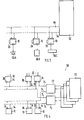
- the interface module 10 contains an assembly 12 for connection to a plurality of connection parts (not shown in FIG. 1), an assembly 14 for producing a multiplicity of connection paths, an assembly 20 for controlling the flow of information on an internal bus 22 and an interface assembly 24 via which is connected to at least one microcomputer 26 (also not shown in FIG. 1).
- the assembly 14 contains a coupling device 16 and a control device 18.
- the module 12 contains a number of serial inputs / outputs (ports) 28 for connection to a plurality of connection parts.
- Each serial input / output 28 contains a converter 30 and a buffer memory 32.
- the converter 30 consists of an input-side series-parallel converter and an output-side parallel-series converter.
- the buffer memory 32 is used to adapt the clock to the internal bus 22.
- a special embodiment shown in FIG. 2 has seven serial inputs / outputs. Among them are a first and a second full duplex input / output 34 or 36. These are provided for standard PCM signals according to CCITT. They work asynchronously with each other. For reasons of reliability, two identical full-duplex inputs / outputs 34 and 36 are present. Each of the two input outputs 34 and 36 has a clock input CLKA or CLKB. In module 20, one of the clocks present at these two clock inputs is selected. Each of the two full-duplex inputs / outputs 34 and 36 has a large number of bidirectional transmission channels. For example, there can be 32 transmission channels per input / output, which can be used to transmit at a transmission speed of more than 4 Mbit / s.
- a third and a fourth full duplex input / output 38 or 40 as well as a simplex output 4 2 (fifth input / output) are also present in the interface module 10. These are used for the direct connection of subscriber devices, such as telephone subscriber devices or computer terminals. They can be set to a variety of transmission speeds and each have a number of independent channels. The interface module 10 is thus able to communicate with almost all current and future digital devices.
- sixth and seventh full duplex inputs / outputs 44 and 46 respectively.
- One channel per data frame leads over both.
- the number of devices that can be connected to the interface module 10 is thus expanded to include devices with a different word length. For example, devices with 64 KBd and 128 KBd can be connected to it.
- These inputs / outputs can be used to transmit data to the relatively slow terminals connected to them in a manner that corresponds to a continuous data stream, ie either with 8 or with 16 bits in a 125 ps data frame.
- the serial inputs / outputs 28 are connected to the internal bus 22, which takes care of the data transport within the interface module 10 in time division multiplexing (TDM).
- TDM time division multiplexing
- the internal bus 22 is divided into 512 time slots per data frame by the clock input via the clock input CLKA or CLKB
- Data frame is divided into 32 channels with 16 time slots each.
- One embodiment provides for a number of time slots per channel, for example five to use for tax purposes. Each time slot can contain 16 bits of information.
- the interface module 10 can be controlled by in-channel signaling in such a way that a large number of message paths can be set up without special control lines to external modules.
- the microcomputer 26 is either an 8-bit or a 16-bit type.
- the interface module 24 includes a silo memory (FIFO) 48 or a module 50 for direct memory access (DMA) or both. Both are available in the example shown.
- a selector switch 51 can be used to switch between them, resulting in two different operating modes.
- the silo memory 48 is selected by a predetermined control signal.
- the notepad memory 52 contains an associative memory (CAM) 56 for the destination, a read-write memory (RAM) 58 in which the data to be transferred are stored and an associative memory (CAM) 60 for the source.
- the control device 54 has a multiplicity of command registers which store commands which precede any information coming in via one of the inputs / outputs 28 or the interface module 24. This means that any channel that leads through any input / output and that delivers a correct command query signal can become the command source. He can then enter or extract data into notepad memory 52 or the various command registers associated therewith.
- Module 20 which controls the flow of information on internal bus 22, includes a master clock for bit-by-bit transmission of data frames on internal bus 22 and synchronizes traffic between controller 54 and notepad memory 52.
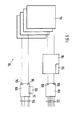
- FIG. 3 shows an application of an interface module 10.
- a transmission system 62 has a number of intermediate lines 64 to which a number of interface modules 10 are connected.
- Each interface module 10 serves one or more peripheral devices 66, for example a plurality of telephone devices 66A, a private branch exchange 66B or a plurality of data terminals 66C.
- the first and second full duplex Inputs / outputs 34 and 36 are each connected to one of the intermediate lines 64.
- the remaining serial inputs / outputs are connected to subscriber terminals.
- the arrangement can be operated such that only certain channels are assigned to each interface module 10 on each intermediate line 64.
- an intermediate line 64 can be provided for transmission purposes and only connected to the first full-duplex inputs / outputs 34 and the other intermediate line 64 can be provided for reception purposes and only connected to the second full-duplex inputs / outputs 36.
- Microcomputers 26 and other digital devices may also be connected.
- data collisions on the intermediate lines 64 can also be avoided by using other methods, for example arbitration methods.
- FIG. 4 shows a switching system 68, which is shown here in one embodiment as a digital switching center with distributed control. It has a digital switching network 70 and a plurality of module control units 72 connected to it. Each module control unit 72 is connected to two intermediate lines 74, which are each designed for 32 PCM channels. In addition, for example, if the switching system 68 is a system 12 switching center of the ITT, the module control unit 72 can deliver signals for clock and frame synchronization to the connected interface modules 10. The data exchange is controlled by the module control unit 72, which establishes the message paths according to their own command and control structure
- each interface module 10 is connected via the first full duplex input / output 34 to the module control unit 72 assigned to it and via the second full duplex input / output 36 to another module control unit 72, if one of the two module control units 72 is excluded Is put into operation, for example in order to bring the program up to date, the subscribers connected to it are connected to the digital switching network 70 via the other module control unit 72. This ensures full redundancy of the module control units for each participant.
- FIG. 5 shows a further messaging system 76. It contains a number of interface modules, as described with reference to FIGS. 1 and 2. They are used here partly as mother (master), partly as daughter (slave).
- a first mother interface module 78 is connected to a transmission section 80.
- a typical transmission section 80 as shown, contains line drivers 81 and various connection lines 83.
- a series of daughter interface modules 84 are connected to the first full-duplex input / output 82 of the first mother interface module 78 via a time-division multiplex PCM line although also via their first full-duplex inputs / outputs 86.
- a second mother interface module 88 is also connected to the transmission section 80, and a number of daughter interface modules 92 are in turn connected to their first full-duplex input / output 90 via their first full-duplex Inputs / outputs 94 are connected.
- a channel is permanently assigned to each daughter interface module 84 and 92.
- the number of daughter interface modules 84 and 92 which can be connected to a mother interface module 78 and 88 is thus limited to the number of channels which can be transmitted via a full duplex input / output.
- the second full-duplex inputs / outputs 96 and 98 of the daughter interface modules 84 and 92 are connected to the first full-duplex inputs / outputs 90 and 82 of the other mother interface module 88 and 78 for reasons of reliability.
- the second full-duplex inputs / outputs 100 and 102 of the mother interface modules 78 and 88 can be connected to further daughter interface modules, switching centers or the like.
- the transmission section 80 can further have third and fourth mother interface modules 104 and 106, respectively.
- these mother interface modules 104 and 106 are connected to local exchanges 108 and 110, respectively, to which a large number of subscribers are connected.
- FIG. 6 shows another switching system 112, the digital switching network 114, a module control unit 116, a first interface module 118, which is connected to the digital switching network 114 via the module control unit 116, and a second interface module 120, which is connected directly to the digital switching network 114 is connected.
- the first interface module 118 establishes connections to a group of participants via a group of lines 122.
- the second interface module 120 establishes further connections to a part of these subscribers via lines 124. Lines 124 are provided for the transmission of packet data.
- the connection between the first interface module 118 and the module control unit 116 preferably takes place via the first and second voliduplex input / output 126 or 128 of the first interface module 118.
- the module control unit 116 contains a first microcomputer 130, from which switch-through connections through the digital Coupling network 114 are built and separated again.
- the second interface module 120 preferably contains a second microcomputer 132, which serves to transmit data packets through the digital switching network 114.
- the second microcomputer 132 is connected to the second interface module 120, preferably via its parallel interface module 2 4 .
- the second interface module 120 is connected to the digital switching network 114 via its first and second full-duplex input / output 134 or 136.
- the switching system 112 described last connects a group of subscribers which are connected to a digital switching network to a packet data network.
Priority Applications (1)
| Application Number | Priority Date | Filing Date | Title |
|---|---|---|---|
| AT85114811T ATE84652T1 (de) | 1984-12-14 | 1985-11-21 | Schnittstellenbaustein zur verbindung von datenquellen mit datensenken und vermittlungssysteme mit solchen schnittstellenbausteinen. |
Applications Claiming Priority (4)
| Application Number | Priority Date | Filing Date | Title |
|---|---|---|---|
| US682038 | 1984-12-14 | ||
| US06/682,228 US4639910A (en) | 1984-12-14 | 1984-12-14 | Apparatus for establishing communication paths |
| US06/682,038 US4638474A (en) | 1984-12-14 | 1984-12-14 | Communication system |
| US682228 | 1984-12-14 |
Publications (3)
| Publication Number | Publication Date |
|---|---|
| EP0185936A2 true EP0185936A2 (fr) | 1986-07-02 |
| EP0185936A3 EP0185936A3 (en) | 1989-04-26 |
| EP0185936B1 EP0185936B1 (fr) | 1993-01-13 |
Family
ID=27102800
Family Applications (1)
| Application Number | Title | Priority Date | Filing Date |
|---|---|---|---|
| EP85114811A Expired - Lifetime EP0185936B1 (fr) | 1984-12-14 | 1985-11-21 | Montage de circuit d'interface pour la connexion de sources de données avec récepteurs de données et systèmes de commutation avec de tels montages de circuit d'interface |
Country Status (3)
| Country | Link |
|---|---|
| EP (1) | EP0185936B1 (fr) |
| AT (1) | ATE84652T1 (fr) |
| DE (1) | DE3586988D1 (fr) |
Cited By (6)
| Publication number | Priority date | Publication date | Assignee | Title |
|---|---|---|---|---|
| EP0193134A2 (fr) * | 1985-02-25 | 1986-09-03 | Alcatel N.V. | Système de commutation avec un réseau de commutation numérique et interface d'abonné pour ce réseau |
| EP0197695A2 (fr) * | 1985-04-03 | 1986-10-15 | Siemens Plessey Electronic Systems Limited | Montages de commutation pour centraux de télécommunication numériques |
| EP0291382A1 (fr) * | 1987-05-15 | 1988-11-17 | Thomson-Csf | Système de commutation numérique |
| EP0325220A1 (fr) * | 1988-01-22 | 1989-07-26 | Alcatel Business Systems | Système de commutation temporelle |
| WO1993012622A1 (fr) * | 1991-12-09 | 1993-06-24 | The Post Office | Equipement terminal de transmission |
| GB2409370A (en) * | 2003-12-20 | 2005-06-22 | Hewlett Packard Development Co | A storage switch and plurality of data sinks |
Families Citing this family (1)
| Publication number | Priority date | Publication date | Assignee | Title |
|---|---|---|---|---|
| DE10202480A1 (de) * | 2001-01-30 | 2002-08-14 | Infineon Technologies Ag | Verfahren und Vorrichtung zur Übertragung eines Signals von einer Signalquelle zu einer Signalsenke in einem System |
Citations (8)
| Publication number | Priority date | Publication date | Assignee | Title |
|---|---|---|---|---|
| CH517419A (de) * | 1970-12-24 | 1971-12-31 | Ibm | Zeitmultiplex-Vermittlungseinrichtung |
| FR2400301A1 (fr) * | 1977-08-08 | 1979-03-09 | Nippon Telegraph & Telephone | Commutateur de voies notamment pour centraux telephoniques numeriques a commutation temporelle |
| GB2006623A (en) * | 1977-10-31 | 1979-05-10 | Straumann Inst Ag | Implant for an artificial tooth |
| GB2016866A (en) * | 1978-03-17 | 1979-09-26 | Int Standard Electric Corp | Multiport digital switching element |
| GB2066623A (en) * | 1979-12-26 | 1981-07-08 | Western Electric Co | Combined data and speech transmission arrangement |
| EP0045066A1 (fr) * | 1980-07-25 | 1982-02-03 | Western Electric Company, Incorporated | Système de commutation à division temporelle |
| GB2097634A (en) * | 1981-04-23 | 1982-11-03 | Western Electric Co | Digital communication system |
| WO1984005003A1 (fr) * | 1983-06-09 | 1984-12-20 | American Telephone & Telegraph | Systeme de commutation de signaux numerises de voix et de donnees a debit multiple |
-
1985
- 1985-11-21 EP EP85114811A patent/EP0185936B1/fr not_active Expired - Lifetime
- 1985-11-21 DE DE8585114811T patent/DE3586988D1/de not_active Expired - Fee Related
- 1985-11-21 AT AT85114811T patent/ATE84652T1/de not_active IP Right Cessation
Patent Citations (8)
| Publication number | Priority date | Publication date | Assignee | Title |
|---|---|---|---|---|
| CH517419A (de) * | 1970-12-24 | 1971-12-31 | Ibm | Zeitmultiplex-Vermittlungseinrichtung |
| FR2400301A1 (fr) * | 1977-08-08 | 1979-03-09 | Nippon Telegraph & Telephone | Commutateur de voies notamment pour centraux telephoniques numeriques a commutation temporelle |
| GB2006623A (en) * | 1977-10-31 | 1979-05-10 | Straumann Inst Ag | Implant for an artificial tooth |
| GB2016866A (en) * | 1978-03-17 | 1979-09-26 | Int Standard Electric Corp | Multiport digital switching element |
| GB2066623A (en) * | 1979-12-26 | 1981-07-08 | Western Electric Co | Combined data and speech transmission arrangement |
| EP0045066A1 (fr) * | 1980-07-25 | 1982-02-03 | Western Electric Company, Incorporated | Système de commutation à division temporelle |
| GB2097634A (en) * | 1981-04-23 | 1982-11-03 | Western Electric Co | Digital communication system |
| WO1984005003A1 (fr) * | 1983-06-09 | 1984-12-20 | American Telephone & Telegraph | Systeme de commutation de signaux numerises de voix et de donnees a debit multiple |
Non-Patent Citations (3)
| Title |
|---|
| ELECTRICAL COMMUNICATION, Band 56, Nr. 1, 1981, Seiten 44-56, Harlow, GB; G. TOLUSSO et al.: "Application of distributed control to handling non-voice services". * |
| ELECTRICAL COMMUNICATION, Band 59, Nr. 1/2, 1985, Seiten 112-119; Harlow, GB; A. CHALET et al.: "System 12: Data module architecture including packet operation". * |
| ELEKTRONICA, Band 32, Nr. 5, März 1984, Seiten 23-32, Deventer, NL, F.M. VAN DER VOORT: "System 12: Opmars van digitale centrales; Deel 2: Systeemarchitecture en technologie". * |
Cited By (12)
| Publication number | Priority date | Publication date | Assignee | Title |
|---|---|---|---|---|
| EP0193134A2 (fr) * | 1985-02-25 | 1986-09-03 | Alcatel N.V. | Système de commutation avec un réseau de commutation numérique et interface d'abonné pour ce réseau |
| EP0193134A3 (fr) * | 1985-02-25 | 1989-03-15 | Alcatel N.V. | Système de commutation avec un réseau de commutation numérique et interface d'abonné pour ce réseau |
| EP0197695A2 (fr) * | 1985-04-03 | 1986-10-15 | Siemens Plessey Electronic Systems Limited | Montages de commutation pour centraux de télécommunication numériques |
| EP0197695A3 (en) * | 1985-04-03 | 1989-04-26 | Plessey Overseas Limited | Switching arrangements for digital telecommunications exchange systems |
| EP0291382A1 (fr) * | 1987-05-15 | 1988-11-17 | Thomson-Csf | Système de commutation numérique |
| FR2615341A1 (fr) * | 1987-05-15 | 1988-11-18 | Thomson Csf | Systeme de commutation numerique |
| US4866700A (en) * | 1987-05-15 | 1989-09-12 | Thomson-Csf | Digital switching system |
| EP0325220A1 (fr) * | 1988-01-22 | 1989-07-26 | Alcatel Business Systems | Système de commutation temporelle |
| FR2626426A1 (fr) * | 1988-01-22 | 1989-07-28 | Telephonie Ind Commerciale | Systeme de commutation temporelle |
| WO1993012622A1 (fr) * | 1991-12-09 | 1993-06-24 | The Post Office | Equipement terminal de transmission |
| US5550913A (en) * | 1991-12-09 | 1996-08-27 | The Post Office | Network terminating unit for connecting analog and digital communication systems to a digital network |
| GB2409370A (en) * | 2003-12-20 | 2005-06-22 | Hewlett Packard Development Co | A storage switch and plurality of data sinks |
Also Published As
| Publication number | Publication date |
|---|---|
| EP0185936A3 (en) | 1989-04-26 |
| EP0185936B1 (fr) | 1993-01-13 |
| ATE84652T1 (de) | 1993-01-15 |
| DE3586988D1 (de) | 1993-02-25 |
Similar Documents
| Publication | Publication Date | Title |
|---|---|---|
| DE2848255C2 (fr) | ||
| EP0156339A2 (fr) | Méthode et dispositif pour la réalisation et l'opération d'une liaison multiplex temporelle à large bande dans un central de commutation à division dans le temps | |
| DE3344140A1 (de) | Nachrichtenuebertragungsanlage mit zwei sammelleitungen | |
| DE3232600C2 (fr) | ||
| DE2249371C2 (de) | Zeitvielfachvermittlungsanlage | |
| EP0186141A2 (fr) | Multiplexeur démultiplexeur avec répartiteur de canaux pour signaux numériques de différents niveaux de hiérarchie | |
| EP0692893A1 (fr) | Dispositif de commutation dans un réseau de commutation numérique à mode de transfer asynchrone | |
| EP0515980B1 (fr) | Etage de commutation temps-espace | |
| EP0185936B1 (fr) | Montage de circuit d'interface pour la connexion de sources de données avec récepteurs de données et systèmes de commutation avec de tels montages de circuit d'interface | |
| EP0193134A2 (fr) | Système de commutation avec un réseau de commutation numérique et interface d'abonné pour ce réseau | |
| DE3336641C2 (de) | Schaltungsanordnung zur steuerbaren Verbindungsherstellung in einer PCM-Vermittlungsanlage | |
| DE2306253B2 (de) | Verfahren zur Durchschaltung von Koppelpunkten in einer PCM-Vermittlungsstelle | |
| DE69734864T2 (de) | Verfahren zur Zuordnung von Zeitsschlitzen in einer Zeitmultiplex-Kommunikationsanlage | |
| EP0264890B1 (fr) | Montage de circuit pour une installation de télécommunication, en particulier un central téléphonique privé avec des ensembles d'interfaces | |
| DE2431256A1 (de) | Zeitvielfachvermittlungsstelle | |
| CH656276A5 (de) | Verfahren und schaltungsanordnung zum uebertragen von datensignalen zwischen datenvermittlungseinrichtungen einer datenvermittlungsanlage. | |
| EP0173274A2 (fr) | Méthode et montage pour la réalisation et la maintenance d'une liaison à division temporelle à large bande | |
| DE4221187A1 (de) | Raum- und Zeit-Vermittlungselement und dessen Verwendung | |
| EP0110360B1 (fr) | Montage de circuit pour rassembler et séparer des signaux de parole et des données lors de la transmission à travers un réseau de commutation numérique | |
| EP0343319B1 (fr) | Procédé de transmission d'informations numériques pour systèmes de commutation de communications | |
| DE2652920A1 (de) | Mehrstufige koppeleinrichtung fuer zeitvielfachbetrieb | |
| DE2909762C2 (de) | PCM-Fernmeldevermittlungsanlage | |
| DE60211823T2 (de) | Master-Slave-Kommunikationssystem und -verfahren für ein Netzwerkelement | |
| DE3937737C2 (de) | Anschlußschaltung an das Netzwerk eines digitalen Nachrichtenübertragungssystems mit Vielfachzugriff im Zeitmultiplex | |
| DE3121774C2 (fr) |
Legal Events
| Date | Code | Title | Description |
|---|---|---|---|
| PUAI | Public reference made under article 153(3) epc to a published international application that has entered the european phase |
Free format text: ORIGINAL CODE: 0009012 |
|
| AK | Designated contracting states |
Kind code of ref document: A2 Designated state(s): AT DE FR GB IT LU NL SE |
|
| RBV | Designated contracting states (corrected) |
Designated state(s): AT DE FR GB IT NL SE |
|
| RAP1 | Party data changed (applicant data changed or rights of an application transferred) |
Owner name: ALCATEL N.V. |
|
| RAP3 | Party data changed (applicant data changed or rights of an application transferred) |
Owner name: ALCATEL N.V. |
|
| PUAL | Search report despatched |
Free format text: ORIGINAL CODE: 0009013 |
|
| AK | Designated contracting states |
Kind code of ref document: A3 Designated state(s): AT DE FR GB IT NL SE |
|
| 17P | Request for examination filed |
Effective date: 19891013 |
|
| 17Q | First examination report despatched |
Effective date: 19910131 |
|
| GRAA | (expected) grant |
Free format text: ORIGINAL CODE: 0009210 |
|
| AK | Designated contracting states |
Kind code of ref document: B1 Designated state(s): AT DE FR GB IT NL SE |
|
| REF | Corresponds to: |
Ref document number: 84652 Country of ref document: AT Date of ref document: 19930115 Kind code of ref document: T |
|
| REF | Corresponds to: |
Ref document number: 3586988 Country of ref document: DE Date of ref document: 19930225 |
|
| GBT | Gb: translation of ep patent filed (gb section 77(6)(a)/1977) |
Effective date: 19930129 |
|
| ITF | It: translation for a ep patent filed |
Owner name: DOTT. ANTONIO SERGI |
|
| ET | Fr: translation filed | ||
| PLBE | No opposition filed within time limit |
Free format text: ORIGINAL CODE: 0009261 |
|
| STAA | Information on the status of an ep patent application or granted ep patent |
Free format text: STATUS: NO OPPOSITION FILED WITHIN TIME LIMIT |
|
| 26N | No opposition filed | ||
| PGFP | Annual fee paid to national office [announced via postgrant information from national office to epo] |
Ref country code: NL Payment date: 19941130 Year of fee payment: 10 |
|
| EAL | Se: european patent in force in sweden |
Ref document number: 85114811.4 |
|
| PGFP | Annual fee paid to national office [announced via postgrant information from national office to epo] |
Ref country code: AT Payment date: 19951109 Year of fee payment: 11 |
|
| PG25 | Lapsed in a contracting state [announced via postgrant information from national office to epo] |
Ref country code: NL Effective date: 19960601 |
|
| NLV4 | Nl: lapsed or anulled due to non-payment of the annual fee |
Effective date: 19960601 |
|
| PG25 | Lapsed in a contracting state [announced via postgrant information from national office to epo] |
Ref country code: AT Effective date: 19961121 |
|
| PGFP | Annual fee paid to national office [announced via postgrant information from national office to epo] |
Ref country code: GB Payment date: 19981012 Year of fee payment: 14 Ref country code: FR Payment date: 19981012 Year of fee payment: 14 |
|
| PGFP | Annual fee paid to national office [announced via postgrant information from national office to epo] |
Ref country code: SE Payment date: 19981022 Year of fee payment: 14 Ref country code: DE Payment date: 19981022 Year of fee payment: 14 |
|
| PG25 | Lapsed in a contracting state [announced via postgrant information from national office to epo] |
Ref country code: GB Free format text: LAPSE BECAUSE OF NON-PAYMENT OF DUE FEES Effective date: 19991121 |
|
| PG25 | Lapsed in a contracting state [announced via postgrant information from national office to epo] |
Ref country code: SE Free format text: LAPSE BECAUSE OF NON-PAYMENT OF DUE FEES Effective date: 19991122 |
|
| GBPC | Gb: european patent ceased through non-payment of renewal fee |
Effective date: 19991121 |
|
| EUG | Se: european patent has lapsed |
Ref document number: 85114811.4 |
|
| PG25 | Lapsed in a contracting state [announced via postgrant information from national office to epo] |
Ref country code: FR Free format text: LAPSE BECAUSE OF NON-PAYMENT OF DUE FEES Effective date: 20000731 |
|
| PG25 | Lapsed in a contracting state [announced via postgrant information from national office to epo] |
Ref country code: DE Free format text: LAPSE BECAUSE OF NON-PAYMENT OF DUE FEES Effective date: 20000901 |
|
| REG | Reference to a national code |
Ref country code: FR Ref legal event code: ST |