EP0176088B1 - Equal distribution density process - Google Patents
Equal distribution density process Download PDFInfo
- Publication number
- EP0176088B1 EP0176088B1 EP85112136A EP85112136A EP0176088B1 EP 0176088 B1 EP0176088 B1 EP 0176088B1 EP 85112136 A EP85112136 A EP 85112136A EP 85112136 A EP85112136 A EP 85112136A EP 0176088 B1 EP0176088 B1 EP 0176088B1
- Authority
- EP
- European Patent Office
- Prior art keywords
- artwork
- sheet
- generating
- film
- master
- Prior art date
- Legal status (The legal status is an assumption and is not a legal conclusion. Google has not performed a legal analysis and makes no representation as to the accuracy of the status listed.)
- Expired - Lifetime
Links
Images


Classifications
-
- H—ELECTRICITY
- H05—ELECTRIC TECHNIQUES NOT OTHERWISE PROVIDED FOR
- H05K—PRINTED CIRCUITS; CASINGS OR CONSTRUCTIONAL DETAILS OF ELECTRIC APPARATUS; MANUFACTURE OF ASSEMBLAGES OF ELECTRICAL COMPONENTS
- H05K3/00—Apparatus or processes for manufacturing printed circuits
-
- H—ELECTRICITY
- H05—ELECTRIC TECHNIQUES NOT OTHERWISE PROVIDED FOR
- H05K—PRINTED CIRCUITS; CASINGS OR CONSTRUCTIONAL DETAILS OF ELECTRIC APPARATUS; MANUFACTURE OF ASSEMBLAGES OF ELECTRICAL COMPONENTS
- H05K3/00—Apparatus or processes for manufacturing printed circuits
- H05K3/0002—Apparatus or processes for manufacturing printed circuits for manufacturing artworks for printed circuits
-
- G—PHYSICS
- G03—PHOTOGRAPHY; CINEMATOGRAPHY; ANALOGOUS TECHNIQUES USING WAVES OTHER THAN OPTICAL WAVES; ELECTROGRAPHY; HOLOGRAPHY
- G03C—PHOTOSENSITIVE MATERIALS FOR PHOTOGRAPHIC PURPOSES; PHOTOGRAPHIC PROCESSES, e.g. CINE, X-RAY, COLOUR, STEREO-PHOTOGRAPHIC PROCESSES; AUXILIARY PROCESSES IN PHOTOGRAPHY
- G03C5/00—Photographic processes or agents therefor; Regeneration of such processing agents
- G03C5/02—Sensitometric processes, e.g. determining sensitivity, colour sensitivity, gradation, graininess, density; Making sensitometric wedges
-
- G—PHYSICS
- G03—PHOTOGRAPHY; CINEMATOGRAPHY; ANALOGOUS TECHNIQUES USING WAVES OTHER THAN OPTICAL WAVES; ELECTROGRAPHY; HOLOGRAPHY
- G03F—PHOTOMECHANICAL PRODUCTION OF TEXTURED OR PATTERNED SURFACES, e.g. FOR PRINTING, FOR PROCESSING OF SEMICONDUCTOR DEVICES; MATERIALS THEREFOR; ORIGINALS THEREFOR; APPARATUS SPECIALLY ADAPTED THEREFOR
- G03F1/00—Originals for photomechanical production of textured or patterned surfaces, e.g., masks, photo-masks, reticles; Mask blanks or pellicles therefor; Containers specially adapted therefor; Preparation thereof
- G03F1/36—Masks having proximity correction features; Preparation thereof, e.g. optical proximity correction [OPC] design processes
-
- H—ELECTRICITY
- H05—ELECTRIC TECHNIQUES NOT OTHERWISE PROVIDED FOR
- H05K—PRINTED CIRCUITS; CASINGS OR CONSTRUCTIONAL DETAILS OF ELECTRIC APPARATUS; MANUFACTURE OF ASSEMBLAGES OF ELECTRICAL COMPONENTS
- H05K1/00—Printed circuits
- H05K1/02—Details
- H05K1/0286—Programmable, customizable or modifiable circuits
- H05K1/0292—Programmable, customizable or modifiable circuits having a modifiable lay-out, i.e. adapted for engineering changes or repair
-
- H—ELECTRICITY
- H05—ELECTRIC TECHNIQUES NOT OTHERWISE PROVIDED FOR
- H05K—PRINTED CIRCUITS; CASINGS OR CONSTRUCTIONAL DETAILS OF ELECTRIC APPARATUS; MANUFACTURE OF ASSEMBLAGES OF ELECTRICAL COMPONENTS
- H05K2203/00—Indexing scheme relating to apparatus or processes for manufacturing printed circuits covered by H05K3/00
- H05K2203/05—Patterning and lithography; Masks; Details of resist
- H05K2203/0548—Masks
- H05K2203/056—Using an artwork, i.e. a photomask for exposing photosensitive layers
-
- H—ELECTRICITY
- H05—ELECTRIC TECHNIQUES NOT OTHERWISE PROVIDED FOR
- H05K—PRINTED CIRCUITS; CASINGS OR CONSTRUCTIONAL DETAILS OF ELECTRIC APPARATUS; MANUFACTURE OF ASSEMBLAGES OF ELECTRICAL COMPONENTS
- H05K2203/00—Indexing scheme relating to apparatus or processes for manufacturing printed circuits covered by H05K3/00
- H05K2203/15—Position of the PCB during processing
- H05K2203/1572—Processing both sides of a PCB by the same process; Providing a similar arrangement of components on both sides; Making interlayer connections from two sides
-
- H—ELECTRICITY
- H05—ELECTRIC TECHNIQUES NOT OTHERWISE PROVIDED FOR
- H05K—PRINTED CIRCUITS; CASINGS OR CONSTRUCTIONAL DETAILS OF ELECTRIC APPARATUS; MANUFACTURE OF ASSEMBLAGES OF ELECTRICAL COMPONENTS
- H05K3/00—Apparatus or processes for manufacturing printed circuits
- H05K3/10—Apparatus or processes for manufacturing printed circuits in which conductive material is applied to the insulating support in such a manner as to form the desired conductive pattern
- H05K3/108—Apparatus or processes for manufacturing printed circuits in which conductive material is applied to the insulating support in such a manner as to form the desired conductive pattern by semi-additive methods; masks therefor
Definitions
- This invention relates to printed wiring boards (PWB) and more particularly to systems and methods for fabricating such boards.
- CAD computer aided design
- Such CAD systems are used to provide a digitized output on a magnetic media.
- the output is in turn applied as an input to photoplotting equipment which generates the PWB artwork.
- the artwork is then used to fabricate the prototype or production version of the printed wiring board by employing well known photography and manufacturing steps.
- circuit board design artworks developed for a panel plate operation to facilitate boards using a pattern plate process
- significant plating unbalances result.
- One technique used to reduce such imbalances has been to take circuit pattern densities into account during the design phase. In addition to restricting the designer, it requires expenditure of extra effort to ensure circuit patterns are uniformly distributed adding to design complexity as well as manually lengthening the design phase.
- a preferred embodiment includes a computer aided design system operative to generate the circuit design patterns for an existing master artwork and an equal density distribution pattern (EDDP).
- the equal density distribution master has a predetermined uniformly distributed repetitive pattern. In the preferred embodiment, it consists of an array or matrix of square spots of a predetermined size (e.g. 1.25 mm) on a grid of a predetermined size (e.g. 2.5 mm).
- the CAD output is in turn applied to photoplotter equipment which produces a photographic master artwork containing the line representations of the existing printed wiring circuit design and a photographic master of the equal density distribution pattern.
- the design master artwork is enlarged or spread by a predetermined amount.
- the method of the present invention provides significant improvements during fabrication, such as marked improvements in two main areas, flow control during lamination and plating control.
- flow control there is a significant reduction in microvoids, uniformity in panel thickness, minimization in panel warp or twist and a large reduction in the potential for delamination.
- the improvements in plating control produce a balanced density of metal from quadrant to quadrant, side to side and from panel to panel.
- the above provides uniformity in board impedance characteristics and improves board reliability in that it is unlikely to have connector failure caused by board warp and twist, since the boards have uniform thickness (i.e., flat rather than tapered). This consistency eliminates the need to subject boards to continuous inspection and testing.
- Figure 1 is a flow diagram of a preferred embodiment of the system of the present invention.
- Figure 2 is a block diagram illustrating the method performed by the system of Figure 1.
- FIGS 3a through 3f illustrate the different photographic artwork masters generated by the various steps shown in Figure 2.
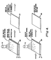
- Figure 4 shows diagrams used to illustrate in greater detail, certain photographic operations performed in Figure 2.
- Figure 5 shows in greater detail, the equal density distribution pattern generated in Figure 2.
- Figure 6 shows a master artwork representative of an existing design used in describing the present invention.
- FIG. 1 is a block diagram of the preferred embodiment of the system which utilizes the method of the present invention.
- the system includes an interactive computer aided design (CAD) system 10.
- CAD computer aided design
- the system 10 is conventional in design and may, for example, take the form of the interactive graphics systems manufactured by Applicon Incorporated.
- the system 10 includes a graphics display terminal unit 12 which includes a keyboard 14 and a tablet 16 with associated electric pen 18.
- a designer can call up an existing source document such as an existing original master artwork. Also, the designer with electronic pen 18 and using the function keys, can generate an array of spots which cover the area of the artwork.
- the system 10 operates to digitize all of the new information pertaining to the EDDP and outputs, the results of the existing design and EDDP separately on magnetic tape. In Figure 1, the separation is illustrated by two magnetic tapes 20 and 22.
- the digitized design and EDDP information, produced on tapes 20 and 22, are applied as an input to a photoplotter 24.
- the photoplotter 24 by activating a photohead element 26 operates to plot the existing design and the EDDP on sheets of an appropriate photographic plastic media.
- the photoplotter 24 is conventional in design and may, for example, take the form of the Model 32B photoplotter manufactured by The Gerber Scientific Instrument Company.
- the master artwork 32 is applied to photographic equipment 42.
- This equipment enlarges or spreads the master artwork image by a predetermined amount as explained herein.
- the equipment can be considered conventional in design and may take the form of the Micro Modifier System, manufactured by Byers Corporation.
- the resulting two masters 30 and 32 are applied to film punch equipment 40 along with the spread master artwork 34.
- the equipment 40 operates to accurately pierce four registration slots in each artwork film in relation to three crosshairs photoplotted on the artworks.
- the equipment 40 includes a surface plate or table onto which a work plate, its pneumatic and electrical components and a manually operated precision X-Y motion system (not shown), are mounted.
- a microscope and camera system (not shown) is mounted on linear bearings above the surface plate on a support. The system microscopes are used to view two orthogonal (alignment) lines on glass plates which are rigidly fixed to the work plate.
- the alignment of artwork on the work plate is accomplished by matching a crosshair plotted on the PWB artwork with a crosshair in a spindle or rotary chuck on the work plate.
- the chuck or spindle is then rotated until the two alignment crosshairs plotted on the PWB artwork coincide with the alignment lines.
- Vaccuum/pneumatic components are used to hold the artwork flat and rigidly in place.
- this equipment is conventional in design and, for example, takes the form of equipment manufactured by Northeastern Tool Company, Inc.
- the punched artworks 30, 32 and 34 are combined photographically in a series of steps on a pinned contact frame table 50.
- the contact frame table 50 is conventional in design and may, for example, take the form of the Model 64A contact printer manufactured by R. W. Borrowdale Company.
- Photoequipment 52 in the form of a light source provides the desired film double exposure required to produce the composite artwork required for the generation of a modified master artwork 36 containing the equal density distribution pattern, as explained herein. Also, the photoequipment 52 includes film developing apparatus conventional in design which is used to process the exposed film.
- the term "artwork” refers to the image or topological layout of the conductor circuit pattern or printed wiring pattern of a printed wiring board on sheet film or glass or other plastic material.
- the upper left quadrant of the board When you have that degree of dissimilarity between quadrants, the upper left quadrant of the board will overplate. That is, during the plating cycle of the fabrication process, the same amount of current is applied to all areas of the entire board. You would need approximately only one-third the amount of current to plate the upper left quadrant as you need for the lower left quadrant. However, this area has two or three time as much current applied to it with the result that etch lines are burned or copper holes are filled. By contrast, the more dense areas of the board are being underplated.
- the process of the present invention not only overcomes these problems, but improves board quality by improving the flow control during lamination and improves plating control.
- microvoids are reduced significantly (i.e., approximately 93 percent)
- the panel thickness is made uniform permitting a reduction in the number of laminate sheets, panel warp is minimized making the boards more reliable and the resulting increase in the amount of metal plated onto the board decreases the potential for delaminations.
- the improved plating control produces a balanced density from quadrant to quadrant, side to side and panel to panel.
- the designer using the CAD system 10 calls up the existing or original master artwork. Also, the designer using CAD system 10 creates the equal density distribution pattern.
- the pattern enlarged and shown in part in Figure 5 consists of a matrix of 1.25 mm x 1.25 mm square spots on a 2.5 mm grid. That is, the designer introduces into the system, X, Y coordinates of all of the pattern. Also, the designer designates the sizes or widths of the lines used to form the spots. The designer creates two separate files, one containing the existing design and the other containing the equal density distribution pattern.
- the CAD system 10 operates to output the manually generated digital information onto two magnetic tapes 20 and 22 of Figure 1. These tapes are applied to the photoplotter 24 of Figure 2 which performs the photographic process of plotting on a first sheet of unexposed photographic film, the lines of the existing design denoted by block 200 of Figure 2. This results in producing the positive master artwork of Figure 3a as denoted by block 202. Also, as part of block 200, photoplotter 24 plots on a second sheet of unexposed photographic film, the equal density distribution pattern (EDDP) according to the present invention. This results in producing the EDDP positive master sheet of Figure 3b, in Figure 2 denoted by block 204.
- EDDP equal density distribution pattern
- a contact copy of the positive master artwork of Figure 3a is made. More specifically, the positive master artwork is placed on contact table 50 over a sheet of unexposed film. Conventional photoequipment exposes film and the master artwork image is developed on the film by the photoequipment.
- the difference between the negative master artwork of Figure 3c and the master artwork of Figure 3a is that the negative master artwork has an opaque background and the circuit pattern is transparent (clear). This produces the negative master artwork (sheet 2 in Figure 2) of Figure 3c.
- the same operation is performed with the EDDP positive master of Figure 3b (sheet 3 in Figure 2). This is denoted by blocks 204 and 207 in Figure 2 and produces the EDDP negative master of Figure 3d (sheet 5 in Figure 2).
- the image on the negative master artwork of Figure 3c is enlarged by 1.25mm (fifty thousandths of an inch) using the photographic equipment 42 of Figure 1. That is, the equipment spreads or expands the line image (etch) of the master artwork which produces the spread positive master artwork of Figure 3e (sheet 4 in Figure 2). This operation is denoted by blocks 210 and 212.
- the positive spread master artwork of Figure 3e (sheet 4), the EDDP negative master of Figure 3d (sheet 5) and a sheet of unexposed photographic plastic media or film (sheet 6 in Figure 2), are punched by the equipment 40 as denoted by block 214. More specifically, in each instance, the sheets of unexposed film and artwork masters are punched so as to include four registration slots. These slots enable the accurate alignment of the artworks and unexposed film during the generation of the required composites pursuant to the steps of blocks 222 through 230 of Figure 2.
- the registration slots are generated by the film punch equipment 40 using the crosshair points appearing on the artworks. The crosshair points are generated by photoplotter 24. Similar registration slots on the sheets of unexposed film are generated by an equivalent fixed punch arrangement (no alignment required for unexposed imageless film).
- a first composite artwork is made by photographically combining the spread positive master artwork of Figure 3e and EDDP negative master of Figure 3d.
- This operation is illustrated diagramatically by block 300 of Figure 4.
- the positive spread master artwork (sheet 4), the negative EDDP master (sheet 5), and the punched unexposed sheet of film (sheet 6) are placed onto pinned contact table 50.
- the film is exposed as denoted by block 224.
- the positive spread master artwork (sheet 4) and the negative EDDP master (sheet 5) are removed while the exposed film (sheet 6) is left as denoted by block 302 in Figure 4.
- a further composite artwork is made by photographically combining the negative master artwork (sheet 2) with the undeveloped exposed film containing the first composite artwork (sheet 6). That is, as shown diagramatically by block 304 of Figure 4, the negative master artwork is placed onto pinned contact frame table 50 over the undeveloped exposed film (sheet 6). The film is then exposed and developed under the control of photoequipment 52. The result is the new positive master artwork of Figure 3f (sheet 7 in Figure 2) which contains the equal density distribution pattern as shown by block 306.
- the resulting modified master artwork contains etch lines of 0.2 mm having 0.525 mm of clearance to any other line, pad or non-functional square spot or pad.
- the double exposure operation places non-functional square spots of the equal density distribution pattern in those areas not covered by circuit line patterns.
- the film (sheet 5) contains a space defined by the spread positive master (sheet 4) cleared from the EDDP negative master (sheet 5) for the actual master artwork circuit line patterns (i.e., 0.2 mm or eight thousandths lines and pads) on the negative master artwork (sheet 2). That is, the combination of a positive image and negative film image eliminated the lines.
- the positive spread master artwork (sheet 4) blocked or restricted the light from being applied to the unexposed film (sheet 6). Thus, it left those areas still sensitive to light (unexposed).
Landscapes
- Engineering & Computer Science (AREA)
- Physics & Mathematics (AREA)
- General Physics & Mathematics (AREA)
- Manufacturing & Machinery (AREA)
- Microelectronics & Electronic Packaging (AREA)
- Exposure And Positioning Against Photoresist Photosensitive Materials (AREA)
- Preparing Plates And Mask In Photomechanical Process (AREA)
- Design And Manufacture Of Integrated Circuits (AREA)
- Manufacture Or Reproduction Of Printing Formes (AREA)
Applications Claiming Priority (2)
| Application Number | Priority Date | Filing Date | Title |
|---|---|---|---|
| US654335 | 1984-09-24 | ||
| US06/654,335 US4627005A (en) | 1984-09-24 | 1984-09-24 | Equal density distribution process |
Publications (3)
| Publication Number | Publication Date |
|---|---|
| EP0176088A2 EP0176088A2 (en) | 1986-04-02 |
| EP0176088A3 EP0176088A3 (en) | 1987-03-18 |
| EP0176088B1 true EP0176088B1 (en) | 1991-07-17 |
Family
ID=24624440
Family Applications (1)
| Application Number | Title | Priority Date | Filing Date |
|---|---|---|---|
| EP85112136A Expired - Lifetime EP0176088B1 (en) | 1984-09-24 | 1985-09-24 | Equal distribution density process |
Country Status (9)
| Country | Link |
|---|---|
| US (1) | US4627005A (enExample) |
| EP (1) | EP0176088B1 (enExample) |
| JP (1) | JPS61105889A (enExample) |
| KR (1) | KR900005307B1 (enExample) |
| AU (1) | AU586640B2 (enExample) |
| CA (1) | CA1232972A (enExample) |
| DE (1) | DE3583475D1 (enExample) |
| FI (1) | FI81690C (enExample) |
| YU (1) | YU172985A (enExample) |
Families Citing this family (3)
| Publication number | Priority date | Publication date | Assignee | Title |
|---|---|---|---|---|
| US4584337A (en) * | 1984-12-18 | 1986-04-22 | Dow Corning Corporation | Aqueous emulsions containing hydrophilic silicone-organic copolymers |
| US7146593B2 (en) * | 2003-11-04 | 2006-12-05 | Freescale Semiconductor, Inc. | Method of implementing polishing uniformity and modifying layout data |
| EP3885961A1 (en) * | 2020-03-26 | 2021-09-29 | Elsyca N.V. | Pcb metal balancing |
Family Cites Families (4)
| Publication number | Priority date | Publication date | Assignee | Title |
|---|---|---|---|---|
| DE2414509C3 (de) * | 1974-03-26 | 1979-02-01 | Siemens Ag, 1000 Berlin Und 8000 Muenchen | Verfahren zur Herstellung von Druckoriginalen für Leiterbahnanordnungen |
| AU2747784A (en) * | 1979-05-24 | 1984-08-16 | Eocom Corp. | Laser image producing system |
| US4336320A (en) * | 1981-03-12 | 1982-06-22 | Honeywell Inc. | Process for dielectric stenciled microcircuits |
| US4571072A (en) * | 1983-09-30 | 1986-02-18 | Honeywell Information Systems Inc. | System and method for making changes to printed wiring boards |
-
1984
- 1984-09-24 US US06/654,335 patent/US4627005A/en not_active Expired - Fee Related
-
1985
- 1985-09-23 AU AU47695/85A patent/AU586640B2/en not_active Ceased
- 1985-09-23 CA CA000491376A patent/CA1232972A/en not_active Expired
- 1985-09-23 FI FI853637A patent/FI81690C/fi not_active IP Right Cessation
- 1985-09-24 EP EP85112136A patent/EP0176088B1/en not_active Expired - Lifetime
- 1985-09-24 JP JP60210908A patent/JPS61105889A/ja active Granted
- 1985-09-24 KR KR1019850007002A patent/KR900005307B1/ko not_active Expired
- 1985-09-24 DE DE8585112136T patent/DE3583475D1/de not_active Expired - Lifetime
- 1985-11-01 YU YU01729/85A patent/YU172985A/xx unknown
Also Published As
| Publication number | Publication date |
|---|---|
| US4627005A (en) | 1986-12-02 |
| CA1232972A (en) | 1988-02-16 |
| KR860002940A (ko) | 1986-04-30 |
| EP0176088A3 (en) | 1987-03-18 |
| FI81690C (fi) | 1990-11-12 |
| FI853637L (fi) | 1986-03-25 |
| YU172985A (en) | 1989-02-28 |
| AU586640B2 (en) | 1989-07-20 |
| KR900005307B1 (ko) | 1990-07-27 |
| AU4769585A (en) | 1986-04-10 |
| FI853637A0 (fi) | 1985-09-23 |
| FI81690B (fi) | 1990-07-31 |
| JPH0431572B2 (enExample) | 1992-05-26 |
| DE3583475D1 (de) | 1991-08-22 |
| JPS61105889A (ja) | 1986-05-23 |
| EP0176088A2 (en) | 1986-04-02 |
Similar Documents
| Publication | Publication Date | Title |
|---|---|---|
| US4897326A (en) | Process to manufacture printed circuit boards | |
| US4571072A (en) | System and method for making changes to printed wiring boards | |
| EP0176088B1 (en) | Equal distribution density process | |
| JPS6142661A (ja) | 露光済フイルムの切断方法 | |
| US3385702A (en) | Photomechanical method of making metallic patterns | |
| US3171741A (en) | Printed wiring layout process | |
| CN85107672A (zh) | 均匀分布密度的加工方法 | |
| DE4007716A1 (de) | Verfahren und vorrichtung zur erstellung einer kopiervorlage | |
| US3782942A (en) | Method for preparing artwork to be used in manufacturing of printed circuits | |
| CA2098844C (en) | Method of cloning printed wiring boards | |
| US3607585A (en) | Printed circuit board artwork pad | |
| US3740225A (en) | Method of making printed circuit boards | |
| JPH04116887A (ja) | 回路パターンの形成方法 | |
| RU2079211C1 (ru) | Способ изготовления печатных плат | |
| Omer | An introduction to laser direct imaging for high density interconnects | |
| US3558312A (en) | Process for fabricating multiple image photographic masters | |
| JP2992081B2 (ja) | パターン作成装置 | |
| SU947976A1 (ru) | Лини дл изготовлени печатных плат | |
| JPH02257696A (ja) | 配線基板の製造方法 | |
| Brody | Large Area Masking Techniques For Thin Film Transistor Arrays | |
| Francis | Profile of the PCB Industry in Scotland | |
| JPS59165494A (ja) | 回路基板の製造方法 | |
| JPS61219954A (ja) | 液晶パネルによるパタ−ン形成方法 | |
| JPH01315749A (ja) | プリント配線基板の原稿原版作成方法 | |
| Zarnow | An introduction to the navy manufacturing technology program for computerized thick-film printing |
Legal Events
| Date | Code | Title | Description |
|---|---|---|---|
| PUAI | Public reference made under article 153(3) epc to a published international application that has entered the european phase |
Free format text: ORIGINAL CODE: 0009012 |
|
| AK | Designated contracting states |
Kind code of ref document: A2 Designated state(s): DE FR GB IT |
|
| PUAL | Search report despatched |
Free format text: ORIGINAL CODE: 0009013 |
|
| AK | Designated contracting states |
Kind code of ref document: A3 Designated state(s): DE FR GB IT |
|
| RAP1 | Party data changed (applicant data changed or rights of an application transferred) |
Owner name: HONEYWELL BULL INC. |
|
| 17P | Request for examination filed |
Effective date: 19870916 |
|
| 17Q | First examination report despatched |
Effective date: 19890224 |
|
| RAP1 | Party data changed (applicant data changed or rights of an application transferred) |
Owner name: BULL HN INFORMATION SYSTEMS INC. |
|
| ITF | It: translation for a ep patent filed | ||
| GRAA | (expected) grant |
Free format text: ORIGINAL CODE: 0009210 |
|
| PGFP | Annual fee paid to national office [announced via postgrant information from national office to epo] |
Ref country code: FR Payment date: 19910712 Year of fee payment: 7 |
|
| AK | Designated contracting states |
Kind code of ref document: B1 Designated state(s): DE FR GB IT |
|
| PGFP | Annual fee paid to national office [announced via postgrant information from national office to epo] |
Ref country code: GB Payment date: 19910725 Year of fee payment: 7 Ref country code: DE Payment date: 19910725 Year of fee payment: 7 |
|
| REF | Corresponds to: |
Ref document number: 3583475 Country of ref document: DE Date of ref document: 19910822 |
|
| ET | Fr: translation filed | ||
| PLBE | No opposition filed within time limit |
Free format text: ORIGINAL CODE: 0009261 |
|
| STAA | Information on the status of an ep patent application or granted ep patent |
Free format text: STATUS: NO OPPOSITION FILED WITHIN TIME LIMIT |
|
| 26N | No opposition filed | ||
| PG25 | Lapsed in a contracting state [announced via postgrant information from national office to epo] |
Ref country code: GB Effective date: 19920924 |
|
| GBPC | Gb: european patent ceased through non-payment of renewal fee |
Effective date: 19920924 |
|
| PG25 | Lapsed in a contracting state [announced via postgrant information from national office to epo] |
Ref country code: FR Effective date: 19930528 |
|
| PG25 | Lapsed in a contracting state [announced via postgrant information from national office to epo] |
Ref country code: DE Effective date: 19930602 |
|
| REG | Reference to a national code |
Ref country code: FR Ref legal event code: ST |