EP0164011B1 - Signalanzeigeeinrichtung, insbesondere für Signalfelder in Gestellen von Digitalsignal- oder Trägerfrequenzsystemen - Google Patents
Signalanzeigeeinrichtung, insbesondere für Signalfelder in Gestellen von Digitalsignal- oder Trägerfrequenzsystemen Download PDFInfo
- Publication number
- EP0164011B1 EP0164011B1 EP85106161A EP85106161A EP0164011B1 EP 0164011 B1 EP0164011 B1 EP 0164011B1 EP 85106161 A EP85106161 A EP 85106161A EP 85106161 A EP85106161 A EP 85106161A EP 0164011 B1 EP0164011 B1 EP 0164011B1
- Authority
- EP
- European Patent Office
- Prior art keywords
- signal
- transistor
- diode
- luminescence
- relay
- Prior art date
- Legal status (The legal status is an assumption and is not a legal conclusion. Google has not performed a legal analysis and makes no representation as to the accuracy of the status listed.)
- Expired
Links
- 230000011664 signaling Effects 0.000 claims abstract description 25
- 238000004020 luminiscence type Methods 0.000 claims abstract 13
- 238000003491 array Methods 0.000 claims abstract 2
- 238000010276 construction Methods 0.000 description 1
- 230000001419 dependent effect Effects 0.000 description 1
- 238000012544 monitoring process Methods 0.000 description 1
- 230000005236 sound signal Effects 0.000 description 1
Images
Classifications
-
- G—PHYSICS
- G08—SIGNALLING
- G08B—SIGNALLING OR CALLING SYSTEMS; ORDER TELEGRAPHS; ALARM SYSTEMS
- G08B5/00—Visible signalling systems, e.g. personal calling systems, remote indication of seats occupied
- G08B5/22—Visible signalling systems, e.g. personal calling systems, remote indication of seats occupied using electric transmission; using electromagnetic transmission
- G08B5/36—Visible signalling systems, e.g. personal calling systems, remote indication of seats occupied using electric transmission; using electromagnetic transmission using visible light sources
-
- G—PHYSICS
- G08—SIGNALLING
- G08B—SIGNALLING OR CALLING SYSTEMS; ORDER TELEGRAPHS; ALARM SYSTEMS
- G08B25/00—Alarm systems in which the location of the alarm condition is signalled to a central station, e.g. fire or police telegraphic systems
- G08B25/14—Central alarm receiver or annunciator arrangements
Definitions
- the invention relates to a signal display device, in particular for signal fields in frames of digital signal or carrier frequency systems, with a series connection of light-emitting diodes for displaying signals and a current source at a signaling voltage, with relays that can be controlled by a signal, with first relay contacts on each Relays, which can cause a short-circuit of the respectively assigned light-emitting diode or a connection to the signaling voltage, and with second relay contacts on each relay as signaling contacts on collecting lines, which lead to a light signaling device, an acoustic signaling device and / or a central operational monitoring.
- Such a signal display device is located in the PCM audio channel system MStD, which is described in the Siemens publication “PCM audio channel system MStD for audio signals with 15 kHz and 7 kHz bandwidth, order no. S42022-A405-A1-2-29.
- error signals are generated as messages from faulty devices and fault signals as messages about the unavailability of message connections. These lead to an urgent alarm (A alarm) or a non-urgent alarm (B alarm), which are displayed in signal fields. Acknowledged lamps are identified by acknowledgment lamps.
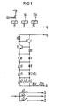
- FIG. 1 shows a signal display device according to the prior art. It contains a relay A, which is excited when there is no A alarm AA, a relay B, which has dropped out when there is no B alarm BA, and a relay C, which has dropped out if there is no reminder signal EA.
- the relays include contacts marked with the corresponding small letter. They are also assigned light-emitting diodes A ', B', C ', which are identified by the same capital letters but with an apostrophe. The light-emitting diode C 'acts as a reminder lamp EL, which only goes out when errors and faults have been eliminated.
- a current source + U s contains transistors T1 and T2 and resistors R1 and R2. Contacts a2, b2 and c2 are signaling contacts via which the states of the A alarm ZA, the B alarm ZB and the reminder signal ZC are signaled.
- a signaling voltage U s between 16 and 72 volts is applied to the series circuit comprising the current source T1, T2, R1, R2, the light-emitting diodes A ', B' and C 'and the contacts a3, b3, c3.
- the transistor T1 then receives a base current through the resistor R1 when one of the contacts a3, b3, c3 is closed.
- the emitter current of this transistor T1 then flows essentially via the resistor R2. If the voltage drop across this resistor R2 reaches a value which is greater than the base-emitter voltage of the transistor T2, then this becomes conductive and reduces the base current of the transistor T1 and thus its emitter current.
- the current flowing through the resistor R2 is therefore essentially dependent on the base-emitter voltage of the transistor T2.
- the current flowing through the resistor R1 depends on the signaling voltage U s and on the number of controlled light-emitting diodes A ', B', C '. As the signaling voltage U s increases, the current through the resistor R1 and thus also the current through the light-emitting diodes A ', B', C ', which is composed of the collector currents of the transistors T1 and T2. Switching on the individual LEDs A ', B' and C 'cause the relay contacts a1, b1, c1, a3, b3, c3.
- the permissible signaling voltage is between 16V and 72V because 24V, 48V and 60V official batteries are available.
- Another signal display device is known from DE-A-2 555 584. This also contains a series connection of LEDs, which can be bridged individually by a switch. A current flows through the series connection both in the display and in the idle state.
- the object of the invention is to extend the permissible range of the signaling voltage U s to 10.5 V to 72 V, to keep the current through the light-emitting diode circuit as constant as possible when it is displayed and to switch it off when it is not displayed, and to make the signal display device cheaper.
- a transistor with an emitter resistor is provided as a current source, that a Zener diode is assigned to the base of the transistor as a reference voltage source, the series resistor of which is connected to a feed input, and that change-over contacts are provided as first relay contacts, which when the in each case associated light-emitting diode directly from the side of the light-emitting diode facing away from the transistor for the light-emitting diode furthest away from the transistor and for the further light-emitting diodes via a decoupling diode to the feed input.
- the expansion of the signaling voltage range has the consequence that the signal display device can also be used in offices with 12V official batteries.
- the current through the light-emitting diodes should remain constant in order to achieve their uniform luminance and in order not to overload the light-emitting diodes due to an impermissibly high increase in the current.
- a relay with a changeover contact is cheaper than one with two individual contacts.
- Zener diode can also be replaced by a series connection of several diodes.
- the zener diode or the series connection of a plurality of diodes it is necessary for the zener diode or the series connection of a plurality of diodes to have a resistor connected in parallel in order to reliably block the transistor when there is no alarm.
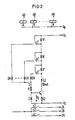
- FIG. 2 shows a signal display device according to the invention for any number of LEDs A '... N'.
- the arrangement contains a corresponding number of relays A ... N, which can be excited via signals AA ... AN.
- the LEDs A '... N' are in series with a current source consisting of a transistor T, the emitter resistor R2 of which consists of a series resistor R1 and a Zener diode Z. This series circuit is connected to a signaling voltage U s .
- the light-emitting diodes A '... N' are bridged in one position by change-over contacts a1 '... n1'. In the other position, they connect the sides of the light-emitting diodes A '...
- the end of the light-emitting diode N 'facing away from the transistor T can either be connected via the diode DN or directly to the feed input S.
- the diodes DA ... D (N - 1) are required, because without them only one LED would light up if several relays responded at the same time.
- the decoupling diodes DA ... DN also ensure that the current through resistor R1 is always the same, regardless of whether one or more relays A ... N have responded.
- the current ILD from the current source T, R2, Z, R1 is equal to zero if no relay A ... N has picked up, since the transistor T then receives no base current via the resistor R1. If one or more relays A ... N have responded, a current flows through the corresponding LED where U z is the Zener voltage and U SE is the base emitter voltage of the transistor T.
- the current I LD is largely independent of the size of the signaling voltage U s , since the Zener voltage U z changes only slightly through the Zener current, which is determined by the value of the resistor R1.
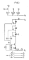
- FIG. 3 shows a signal display device according to the invention, which meets the requirements of the specified specifications of the Irish Bureaupost.
- the arrangement corresponds in principle to that of FIG. 2.
- a zener diode instead of a zener diode, a series connection of three diodes D1 ... D3 is provided, to which a resistor R3 is connected in parallel.
- Resistor R1 has a value of 10 kOhm
- resistor R2 has a value of 121 Ohm
- resistor R3 has a value of 100 kOhm.
- the transistor T is of the type 2N3440.
Landscapes
- Physics & Mathematics (AREA)
- General Physics & Mathematics (AREA)
- Electromagnetism (AREA)
- Business, Economics & Management (AREA)
- Emergency Management (AREA)
- Audible And Visible Signals (AREA)
- Color Television Systems (AREA)
- Control Of El Displays (AREA)
- Led Device Packages (AREA)
- Control Of Indicators Other Than Cathode Ray Tubes (AREA)
- Radar Systems Or Details Thereof (AREA)
- Circuits Of Receivers In General (AREA)
- Electronic Switches (AREA)
- Input Circuits Of Receivers And Coupling Of Receivers And Audio Equipment (AREA)
Priority Applications (1)
| Application Number | Priority Date | Filing Date | Title |
|---|---|---|---|
| AT85106161T ATE36615T1 (de) | 1984-05-22 | 1985-05-20 | Signalanzeigeeinrichtung, insbesondere fuer signalfelder in gestellen von digitalsignaloder traegerfrequenzsystemen. |
Applications Claiming Priority (2)
| Application Number | Priority Date | Filing Date | Title |
|---|---|---|---|
| DE3419041 | 1984-05-22 | ||
| DE3419041 | 1984-05-22 |
Publications (2)
| Publication Number | Publication Date |
|---|---|
| EP0164011A1 EP0164011A1 (de) | 1985-12-11 |
| EP0164011B1 true EP0164011B1 (de) | 1988-08-17 |
Family
ID=6236554
Family Applications (1)
| Application Number | Title | Priority Date | Filing Date |
|---|---|---|---|
| EP85106161A Expired EP0164011B1 (de) | 1984-05-22 | 1985-05-20 | Signalanzeigeeinrichtung, insbesondere für Signalfelder in Gestellen von Digitalsignal- oder Trägerfrequenzsystemen |
Country Status (9)
| Country | Link |
|---|---|
| EP (1) | EP0164011B1 (enExample) |
| JP (1) | JPS60254297A (enExample) |
| AT (1) | ATE36615T1 (enExample) |
| AU (1) | AU553737B2 (enExample) |
| BR (1) | BR8502399A (enExample) |
| DE (1) | DE3564500D1 (enExample) |
| GR (2) | GR80729B (enExample) |
| MX (1) | MX158915A (enExample) |
| NO (1) | NO164267C (enExample) |
Families Citing this family (1)
| Publication number | Priority date | Publication date | Assignee | Title |
|---|---|---|---|---|
| JP6427873B2 (ja) | 2013-12-20 | 2018-11-28 | 株式会社Ihi | 駐車支援装置及びシステム |
Family Cites Families (4)
| Publication number | Priority date | Publication date | Assignee | Title |
|---|---|---|---|---|
| US3643244A (en) * | 1969-05-26 | 1972-02-15 | Marvin J Levy | Fire and smoke monitoring and alarm system |
| DE2555584A1 (de) * | 1975-12-10 | 1977-06-16 | Siemens Ag | Anzeigetafel mit mehreren leuchtdioden |
| JPS5834549Y2 (ja) * | 1977-11-09 | 1983-08-03 | 横河電機株式会社 | 多点表示装置 |
| JPS556687A (en) * | 1978-06-29 | 1980-01-18 | Handotai Kenkyu Shinkokai | Traffic use display |
-
1984
- 1984-10-22 GR GR80729A patent/GR80729B/el unknown
-
1985
- 1985-05-20 GR GR851215A patent/GR851215B/el unknown
- 1985-05-20 DE DE8585106161T patent/DE3564500D1/de not_active Expired
- 1985-05-20 AT AT85106161T patent/ATE36615T1/de not_active IP Right Cessation
- 1985-05-20 MX MX205346A patent/MX158915A/es unknown
- 1985-05-20 EP EP85106161A patent/EP0164011B1/de not_active Expired
- 1985-05-21 AU AU42693/85A patent/AU553737B2/en not_active Ceased
- 1985-05-21 BR BR8502399A patent/BR8502399A/pt not_active IP Right Cessation
- 1985-05-22 JP JP60108486A patent/JPS60254297A/ja active Granted
- 1985-05-22 NO NO852053A patent/NO164267C/no unknown
Also Published As
| Publication number | Publication date |
|---|---|
| NO852053L (no) | 1985-11-25 |
| AU553737B2 (en) | 1986-07-24 |
| JPH0510715B2 (enExample) | 1993-02-10 |
| EP0164011A1 (de) | 1985-12-11 |
| GR80729B (en) | 1985-02-20 |
| GR851215B (enExample) | 1985-11-25 |
| BR8502399A (pt) | 1986-01-21 |
| ATE36615T1 (de) | 1988-09-15 |
| NO164267C (no) | 1990-09-12 |
| JPS60254297A (ja) | 1985-12-14 |
| DE3564500D1 (en) | 1988-09-22 |
| MX158915A (es) | 1989-03-29 |
| NO164267B (no) | 1990-06-05 |
| AU4269385A (en) | 1985-11-28 |
Similar Documents
| Publication | Publication Date | Title |
|---|---|---|
| DE3044203A1 (de) | Automatisches nebenschlusssystem | |
| DE2817121C2 (de) | Gefahrenmeldeanlage | |
| EP2428942B1 (de) | Gefahrenmeldeanlage mit zwei Datenübertragungsgeschwindigkeiten | |
| EP0164011B1 (de) | Signalanzeigeeinrichtung, insbesondere für Signalfelder in Gestellen von Digitalsignal- oder Trägerfrequenzsystemen | |
| WO2007017073A2 (de) | Gebäudeleittechnik- oder gefahrenmeldeanlage | |
| DE2749401C2 (enExample) | ||
| EP0164014B1 (de) | Anordnung zur Anregung von Relais | |
| EP0500201B1 (de) | Schaltung zum Überwachen wechselstromgespeister Signallampen | |
| EP0171468A2 (de) | Sendeschaltung für Signalübertragungssysteme | |
| DE3643226A1 (de) | Einrichtung zum signaltechnisch sicheren betrieb mehrerer elektrischer verbraucher | |
| DE2903266C2 (de) | Gefahrenmeldeanlage | |
| DE2547938C3 (de) | Verfahren zur Prüfung von Leitungen in Geräten der Nachrichtentechnik und Schaltungsanordnung zur Durchführung des Verfahrens | |
| DE1540628C3 (de) | Abfrageeinrichtung für die Kontaktstellung von Meldeschaltern | |
| DE533445C (de) | Schaltungsanordnung fuer selbsttaetige und halbselbsttaetige Fernsprechanlagen mit Speichern | |
| DE1562121B2 (de) | Schaltungsanordnung fuer eine koppelanordnung | |
| DE1915186B2 (de) | Geraeteanordnung fuer einrichtungen der nachrichtenuebertragungstechnik | |
| DE19905708C1 (de) | Verfahren zur Administration von zusammengehörenden PCM-Kanälen für Mehrkanalverbindungen | |
| EP0211213A1 (de) | Anordnung zur Überwachung eines PCM- oder DS-Geräts oder eines Digitalsignal-Kanalverteilers für n-bit-Multiplexsignale | |
| DE2910500C2 (de) | Anordnung zur Ortung von Unterbrechungen in Nachrichten-Übertragungsleitungen | |
| DE2360722C2 (de) | Schaltungsanordnung als Versorgungs- und Verbindungsglied zwischen elektrischen Kontakten und einer deren Schaltzustand auswertenden Auswerteschaltung | |
| DE2532239C3 (de) | Kreuzschienenverteiler | |
| DE2046945C (de) | Elektronische Schalteinrichtung | |
| DE3002771C2 (de) | Erdschlußrelais | |
| DE1286584B (de) | UEberwachungseinrichtung fuer mehrere Sicherungen | |
| AT206016B (de) | Elektronischer Umwerter für Kennzahlen verschiedener Stellenzahl in Fernmeldeanlagen |
Legal Events
| Date | Code | Title | Description |
|---|---|---|---|
| PUAI | Public reference made under article 153(3) epc to a published international application that has entered the european phase |
Free format text: ORIGINAL CODE: 0009012 |
|
| AK | Designated contracting states |
Designated state(s): AT BE CH DE FR GB IT LI NL SE |
|
| 17P | Request for examination filed |
Effective date: 19860128 |
|
| 17Q | First examination report despatched |
Effective date: 19870116 |
|
| GRAA | (expected) grant |
Free format text: ORIGINAL CODE: 0009210 |
|
| AK | Designated contracting states |
Kind code of ref document: B1 Designated state(s): AT BE CH DE FR GB IT LI NL SE |
|
| REF | Corresponds to: |
Ref document number: 36615 Country of ref document: AT Date of ref document: 19880915 Kind code of ref document: T |
|
| GBT | Gb: translation of ep patent filed (gb section 77(6)(a)/1977) | ||
| REF | Corresponds to: |
Ref document number: 3564500 Country of ref document: DE Date of ref document: 19880922 |
|
| ET | Fr: translation filed | ||
| ITF | It: translation for a ep patent filed | ||
| PLBE | No opposition filed within time limit |
Free format text: ORIGINAL CODE: 0009261 |
|
| STAA | Information on the status of an ep patent application or granted ep patent |
Free format text: STATUS: NO OPPOSITION FILED WITHIN TIME LIMIT |
|
| 26N | No opposition filed | ||
| ITTA | It: last paid annual fee | ||
| PGFP | Annual fee paid to national office [announced via postgrant information from national office to epo] |
Ref country code: GB Payment date: 19920424 Year of fee payment: 8 Ref country code: AT Payment date: 19920424 Year of fee payment: 8 |
|
| PGFP | Annual fee paid to national office [announced via postgrant information from national office to epo] |
Ref country code: SE Payment date: 19920521 Year of fee payment: 8 Ref country code: FR Payment date: 19920521 Year of fee payment: 8 |
|
| PGFP | Annual fee paid to national office [announced via postgrant information from national office to epo] |
Ref country code: BE Payment date: 19920522 Year of fee payment: 8 |
|
| PGFP | Annual fee paid to national office [announced via postgrant information from national office to epo] |
Ref country code: NL Payment date: 19920531 Year of fee payment: 8 |
|
| PGFP | Annual fee paid to national office [announced via postgrant information from national office to epo] |
Ref country code: DE Payment date: 19920724 Year of fee payment: 8 |
|
| PGFP | Annual fee paid to national office [announced via postgrant information from national office to epo] |
Ref country code: CH Payment date: 19920821 Year of fee payment: 8 |
|
| PG25 | Lapsed in a contracting state [announced via postgrant information from national office to epo] |
Ref country code: GB Effective date: 19930520 Ref country code: AT Effective date: 19930520 |
|
| PG25 | Lapsed in a contracting state [announced via postgrant information from national office to epo] |
Ref country code: SE Effective date: 19930521 |
|
| PG25 | Lapsed in a contracting state [announced via postgrant information from national office to epo] |
Ref country code: LI Effective date: 19930531 Ref country code: CH Effective date: 19930531 Ref country code: BE Effective date: 19930531 |
|
| BERE | Be: lapsed |
Owner name: SIEMENS A.G. BERLIN UND MUNCHEN Effective date: 19930531 |
|
| PG25 | Lapsed in a contracting state [announced via postgrant information from national office to epo] |
Ref country code: NL Effective date: 19931201 |
|
| NLV4 | Nl: lapsed or anulled due to non-payment of the annual fee | ||
| GBPC | Gb: european patent ceased through non-payment of renewal fee |
Effective date: 19930520 |
|
| PG25 | Lapsed in a contracting state [announced via postgrant information from national office to epo] |
Ref country code: FR Effective date: 19940131 |
|
| REG | Reference to a national code |
Ref country code: CH Ref legal event code: PL |
|
| PG25 | Lapsed in a contracting state [announced via postgrant information from national office to epo] |
Ref country code: DE Effective date: 19940201 |
|
| REG | Reference to a national code |
Ref country code: FR Ref legal event code: ST |
|
| EUG | Se: european patent has lapsed |
Ref document number: 85106161.4 Effective date: 19931210 |