EP0153119A2 - Einkristall einer III-V-Halbleiterverbindung mit kleiner Versetzungsdichte - Google Patents
Einkristall einer III-V-Halbleiterverbindung mit kleiner Versetzungsdichte Download PDFInfo
- Publication number
- EP0153119A2 EP0153119A2 EP85300889A EP85300889A EP0153119A2 EP 0153119 A2 EP0153119 A2 EP 0153119A2 EP 85300889 A EP85300889 A EP 85300889A EP 85300889 A EP85300889 A EP 85300889A EP 0153119 A2 EP0153119 A2 EP 0153119A2
- Authority
- EP
- European Patent Office
- Prior art keywords
- impurity
- crystal
- host
- isoelectronic
- impurities
- Prior art date
- Legal status (The legal status is an assumption and is not a legal conclusion. Google has not performed a legal analysis and makes no representation as to the accuracy of the status listed.)
- Granted
Links
Images


Classifications
-
- C—CHEMISTRY; METALLURGY
- C30—CRYSTAL GROWTH
- C30B—SINGLE-CRYSTAL GROWTH; UNIDIRECTIONAL SOLIDIFICATION OF EUTECTIC MATERIAL OR UNIDIRECTIONAL DEMIXING OF EUTECTOID MATERIAL; REFINING BY ZONE-MELTING OF MATERIAL; PRODUCTION OF A HOMOGENEOUS POLYCRYSTALLINE MATERIAL WITH DEFINED STRUCTURE; SINGLE CRYSTALS OR HOMOGENEOUS POLYCRYSTALLINE MATERIAL WITH DEFINED STRUCTURE; AFTER-TREATMENT OF SINGLE CRYSTALS OR A HOMOGENEOUS POLYCRYSTALLINE MATERIAL WITH DEFINED STRUCTURE; APPARATUS THEREFOR
- C30B15/00—Single-crystal growth by pulling from a melt, e.g. Czochralski method
-
- C—CHEMISTRY; METALLURGY
- C30—CRYSTAL GROWTH
- C30B—SINGLE-CRYSTAL GROWTH; UNIDIRECTIONAL SOLIDIFICATION OF EUTECTIC MATERIAL OR UNIDIRECTIONAL DEMIXING OF EUTECTOID MATERIAL; REFINING BY ZONE-MELTING OF MATERIAL; PRODUCTION OF A HOMOGENEOUS POLYCRYSTALLINE MATERIAL WITH DEFINED STRUCTURE; SINGLE CRYSTALS OR HOMOGENEOUS POLYCRYSTALLINE MATERIAL WITH DEFINED STRUCTURE; AFTER-TREATMENT OF SINGLE CRYSTALS OR A HOMOGENEOUS POLYCRYSTALLINE MATERIAL WITH DEFINED STRUCTURE; APPARATUS THEREFOR
- C30B29/00—Single crystals or homogeneous polycrystalline material with defined structure characterised by the material or by their shape
- C30B29/10—Inorganic compounds or compositions
- C30B29/40—AIIIBV compounds wherein A is B, Al, Ga, In or Tl and B is N, P, As, Sb or Bi
-
- Y—GENERAL TAGGING OF NEW TECHNOLOGICAL DEVELOPMENTS; GENERAL TAGGING OF CROSS-SECTIONAL TECHNOLOGIES SPANNING OVER SEVERAL SECTIONS OF THE IPC; TECHNICAL SUBJECTS COVERED BY FORMER USPC CROSS-REFERENCE ART COLLECTIONS [XRACs] AND DIGESTS
- Y10—TECHNICAL SUBJECTS COVERED BY FORMER USPC
- Y10T—TECHNICAL SUBJECTS COVERED BY FORMER US CLASSIFICATION
- Y10T428/00—Stock material or miscellaneous articles
- Y10T428/12—All metal or with adjacent metals
- Y10T428/12493—Composite; i.e., plural, adjacent, spatially distinct metal components [e.g., layers, joint, etc.]
- Y10T428/12528—Semiconductor component
Definitions
- This invention relates to a single crystal of compound semiconductor of groups III-V with low dislocation density.
- the elements of group III on the periodic table are B, Al, Ga, In, etc.
- the elements of group Y are N, P, As, Sb, etc.
- Semiconductors consisting of these elements are GaAs, InSb, GaP, GaSb and other many compounds.
- Compound semiconductors of groups III ⁇ V are used as substrate for field effect transistors, integrated circuits including them, light emitting devices, light detecting devices or various optical integrated circuits.
- Dislocation density signifies the numbers of dislocation of lattices in a single crystal in unit volume. Dislocation density is frequently represented by EPD ( Etch Pit Density ). A single crystal is sliced to thin wafers. A wafer is then etched in a pertinent etchant which reveals superficial dislocations as etch pits. EPD is defined as a number of etch pits per unit area. Operator counts the number of etch pits in a definite area on a wafer through a microscope and calculates EPD by dividing the number by the area.
- EPD Etch Pit Density
- EPD is one of practical representations of dislocation density we give the terms EPD and dislocation density the same meaning from now on.
- dislocation density is low, and the distribution of dislocation density is uniform on a wafer. It may be best, that the distribution of dislocation density is uniform throughout a single crystal ingot.
- GaAs single crystals grown by conventional LEG method have great many dislocations.
- EPD is usually 50,000 to 100,000cm -2 .
- LEG method is one of pulling methods for crystal growth.
- a single crystal is pulled up into B 2 0 3 from a material melt.
- Temperature gradient in the crystal is very large near a solid- liquid interface. Big thermal stress is generated. Great thermal distortions happens by the stress. Preveling thermal distortions multiply dislocations in the single crystal.
- HB method Horizontal Bridgman Method
- HB method Horizontal Bridgman Method
- This invention has a wide applicability for any methods for growing a single crystal of compound semiconductors. Namely it is fully applicable to LEG method, HB method and other methods.
- Most pure metals are soft and weak metals. Hardness and stickiness of metals are heighten by adding impurities. For example, carbon is added to iron to harden it. An alloy is made by mixing different metals.
- one impurity was doped intentionally. In practice more than one impurities may be included in a single crystal, but these impurities other than one impurity were included in material and were not ridded by a refining process.
- Te, Pb, Si and Cr are not the elements of group III or group Y , the electronic property of compound semiconductors of groups III-V is changed by doping with these impurities.
- doping with the elements of group e.g. B, Al, Ga and In or doping with the elements of group V, e.g. N, P, As and Sb does not change the electronic property of compound semiconductors of groups III ⁇ V , because doped impurity atoms are apt to replace the lattice sites which should be occupied by elements of a host crystal having the same valence number.
- the main elements composing the crystal are called " host elements ", and the crystal to be doped with impurities is called " host crystal " from now.
- isoelectronic impurities These impurities which do not change the electronic property of a host crystal are called "isoelectronic impurities ".
- Practical definition of isoelectronic impurity is an impurity which is doped into a compound semiconductor of groups III ⁇ V and is an element belonging to group III or group except host elements.
- impurities Si, Zn, Sn, S, Te, Cr, Pb, etc. which do not belong to group III nor to group V have electronic activities in compounds of groups III ⁇ V. These impurities are called anisoelectronic impurities from now.
- Mixed compound semiconductors are usually made by an epitaxy which forms active layer upon a substrate of compound semiconductor belonging to the same groups.
- the coordination of lattice constants between the substrate and the epitaxial growth layer is a serious problem.
- the difference of lattice constants between InP and InGaAsP should be coordinated to be less than 0.2%.
- the allowable maximum difference of lattice constants is 0.26%.
- the difference of lattice constants would generate misfit dislocations at the boundary between substrate and epitaxial layer.
- the misfit dislocations would propagate into an epitaxial layer and multiply dislocations in the layer.
- micro cracks occur in an InGaSb single crystal, if the difference of lattice constants between the GaSb seed crystal and the pulled InGaSb crystal.
- Jacob's impurity-doped single crystals of compound semiconductors aforementioned had serious difficulties, although EPD were greatly reduced in a confined region of the crystal.
- distribution coefficient is much less than 1.
- impurity is condensed in a melt while crystal growth progresses. Therefore impurity concentration in a grown crystal is lowest at a front end (which is connected with a seed crystal ) and highest at a back end (which is farthest from a seed crystal and is pulled last ).
- the impurity concentration in a crystal is high, for example, 10% even at the front end, the pulled crystal cannot become a single crystal at the back end where impurity is concentrated. Near the back end impurity inclusion occurs on the surface of the crystal. Poly-crystal or crystal with impurity inclusion cannot be used as substrate for electronic devices.
- Wafers must be at least two inches in diameter to be practically used for industrial purposes. Production of such wide wafers is supposed to be several times as difficult as that of small wafers of 15 to 25mm in diameter.
- In inclusion occurs and crystal becomes non-single.
- Such an impurity inclusion near a back end of a crystal also occurs in the case of Sb doping into a GaAs host crystal.
- an effective diameter of an impurity element is larger than that of a host element of the same group which the impurity should replace.
- the bond length of In-As is supposed to be longer than the bond length of Ga-As, because effective diameter of In is larger than that of Ga.
- the other impurities, B, N, P and Al in a GaAs host crystal have effective radius smaller than that of the host elements. Similar assumption would hold in the case of the smaller impurities.
- the bond length of B-As would be shorter than the bond length of Ga-As in the host crystal but longer than the bond length of B-As in a BAs crystal.
- an impurity-doped crystal has not distinctive boundaries which might divide the lattices consisting only of host elements from the lattices including impurity elements unlike an epitaxial layer grown on a substrate or a single crystal grown from a seed crystal. Therefore the lattice misfit in an impurity-doped crystal will differ from the lattice misfit in these matters.
- host elements are Ga and As in the case of a GaAs single crystal. From now we call the impurities which are apt to make a bond longer than the host bond of Ga-As by coupling with one of host elements " over-impurities ". And we call the impurities which are apt to make a bond shorter than the host bond of Ga-As by coupling with one of host elements " under-impurities ".
- B and N are under-impurities.
- Sb and In are over-impurities.
- B, N, Ga, P and Al are under-impurities.
- Sb is an over-impurity.
- the bond length between host elements is denoted by A O'
- the bond length between an under-impurity and a host element is denoted by A 1 .
- the bond length between an over-impurity and a host element is denoted by A 2 .
- a 0 is a bond length of Ga-As
- a 1 is a bond length of N-Ga
- a 2 is a bond length of In-As.
- N 0 is a number of host pairs Ga-As
- N 1 is a number of under-impurity atoms
- N 2 is a number of over-impurity atoms
- u 1 is a quotient of N 1 divided by N 0
- u 2 is a quotient of N 2 divided by N 0 .
- the length "l" of a side of a small region is given by where l is normalized to be a unit when no impurity exists.
- Deviations ⁇ 1 and ⁇ 2 of the bond lengths A 1 and A 2 from the standard bond length A 0 are defined by,
- the deviation ⁇ 1 is negative, but the deviation ⁇ 2 is positive.
- Such contacts are one-dimensional contacts.
- N 0 will be eliminated together with N 1 and N 2 .
- N 1 and N 2 instead of these variables we use the ratios Z 1 and Z 2 of under-impurity and over-impurity to total impurities.
- Z 1 and Z 2 are,
- the ratio of Z 1 to u 1 or Z 2 to u 1 is equal to be a ratio of the number of host atoms to the number of impurity atoms.
- the ratio is supposed to be about 100 to 10000.
- lattice misfit coefficient ⁇ defined by Z 1 and Z 2 instead of Eq.(5) should be smaller than a maximum value which may be 1% to 10%.
- Z 1 and Z 2 in Eq.(11) are ratios.
- the lattice misfit coefficient ⁇ can be defined by impurity concentrations x 1 and x 2 ( atoms / cm 3 ). Then, where x 1 is a concentration of an under-impurity, and x 2 is a concentration of an over-impurity.
- A The arithmetic average of bond lengths of impurity-host bonds is denoted by A .
- the lattice misfit coefficient is a quotient of the difference between the arithmetic average of impurity-bond lengths and the standard bond length divided by the standard bond length.
- the bond lengths A 0 , A 1 and A 2 are the variables depending upon the impurity concentrations. We safely assume the standard bond length A 0 between host elements is equal to the normal standard bond length between host elements in a host crystal without impurity.
- bond lengths A 1 and A 2 are replaced by more definite and measurable bond lengths a 1 and a 2 , which are defined as bond lengths between an impurity atom and a host atom in a pure single crystal of groups III ⁇ V comprising only the elements same with the impurity element and the host element to be coupled with it.
- the bond lengths a 1 and a 2 are definite and known in many cases. But a 1 and a 2 are not equal to A 1 and A 2 .
- the bond length of Ga-As in a GaAs single crystal is 2.44 ⁇ .
- the bond length of In-As in an InAs single crystal is 2.62 ⁇ .
- the impurity bond length A 2 of In-As in a GaAs host crystal shall be replaced by the pure bond length a 2 ( 2.62 A ) of In-As in an InAs crystal.
- the bond length of Ga-As in a GaAs crystal is 2.44 ⁇ .
- the bond length of In-P in an InP crystal is 2.54 ⁇ .
- the bond length of In-As in an InAs crystal is 2.62 ⁇ .
- the bond length of Ga-P in a GaP crystal is 2.36 A .
- Table(l) shows the bond lengths in ⁇ unit between the elements of groups III and V in a pure two-component crystal of groups III ⁇ V.
- the elements of group III are denoted in the uppermost line.
- the elements of group V are denoted in the leftest column.
- the numeral on a cross point of a column and a line shows the bond length between two atoms of groups and V which are captioned in the line and the column.
- This invention requires that the total concentrations of isoelectronic impurities should be more than 10 18 atoms/cm 3 , and the arithmetic average " a " of the bond lengths between isoelectronic impurities and host atoms should not differ from the standard bond length " a 0 " between host atoms by more than plus or minus 2 %.
- Table(2) shows the tetrahedral covalent bond length " a 0 ", " a 1 " and “ a 2 "in ⁇ unit, and the deviations ⁇ 1 ( negative ) or ⁇ 2 ( positive ) by percentage with regard to host crystal and impurities doped therein.
- this invention proposes a single crystal of compound semiconductor of groups III ⁇ V doped with isoelectronic under- and over-impurities, wherein the total concentrations of isoelectronic impurities are more than 1 X 10 13 atoms/cm 3 and the arithmetic average " a " of the bond lengths between isoelectronic impurities and host atoms differs from the standard bond length " a 0 " between host atoms by less than plus or minus two percents.
- At least one isoelectronic over-impurity ( a 2 >a 0 , ⁇ 2 >0 ) and at least one isoelectronic under-impurity ( a 1 ⁇ a 0 , ⁇ 1 ⁇ 0 ) should be doped in a single crystal in order to confine the difference between the arithmetic average " a " and the standard length " a 0 " within plus or minus two percents.
- this invention requires the absolute value of the lattice misfit coefficient ⁇ should be reduced less than 2 % by double doping of isoelectronic under-and over-impurities.
- the lattice misfit coefficient " ⁇ " or the arithmetic average " a " of bond lengths do not correspond to any concrete physical values.
- the lattice misfit coefficient " ⁇ " is the quotient of the product of " e " and impurity concentration ( N 1 + N 2 ) divided by host atom number N 0 .
- FIG.1 shows a three-temperature LEC apparatus for growing a single crystal as an example.
- a crucible(l) made from some pertinent material, e.g. PBN ( pyrolitic boron nitride ) is sustained by a graphite susceptor(2).
- Material melt contains host compounds and impurities. Then we call it compound melt.
- the compound melt is divided in two parts by a floating crucible(7).
- the floating crucible(7) has small holes(8) on the bottom wall.
- the outer melt(4) goes through the small holes(8) into the inner melt(6).
- a liquid encapsulant(5) covers both inner melt(6) and outer melts(4).
- a seed crystal(10) is fixed at the bottom end of an upper shaft(15).
- a single crystal(9) is pulled up by the seed crystal(10) in succession.
- a lower shaft(16) supports the susceptor(2).
- Heating apparatus consists of three heaters arranged in a vertical direction. A lower heater(Hl), a middle heater(H2) and an upper heater(H3) can be controlled independently.
- the three-temperature LEC method was a novel method which was disclosed for the first time in Japanese Patent Application No.154771/83 filed by the Assignee of this invention also.
- the temperature gradient in a liquid encapsulant B 2 0 3 can be 30 to 50 °C/cm and the temperature gradient in an upper space can be lower than 20 C/cm in the case of the crystal growth of GaAs.
- FIG.1 is a very naked LEC apparatus.
- the InP host crystal is doped with an isoelectronic under-impurity Ga, an isoelectronic over-impurity As and an anisoelectronic impurity S.
- the liquid encapsulant is fully- dehydrated B 2 O 3 .
- a floating crucible and an outer crucible are used.
- the InP single crystal is grown along ⁇ 100> direction.
- the distribution coefficients k of As, Ga and S in InP melt and solid are ;
- Ga is added out of the floating crucible, because the distribution coefficient is more than 1.
- An InP single crystal is grown up from the materials by the improved LEG method.
- m is the doping weight of impurity.
- M is the atomic weight of impurity. Then the impurity is doped by ( m/M ) mol. The number of atoms in 1 mol is equal to the Avogadro's number " L 0 ( 6.02 X 10 23 atoms ) ".
- k denotes the distribution coefficient of the impurity.
- m g of impurity is added into “ w “ g of charged polycrystal. Then the materials are heated and molten.
- the impurity concentration " n " in a crystal is
- EPD is usually smaller at front end and bigger at back end in the crystals grown by conventional LEC method.
- the As concentration in the floating crucible is diluting during the crystal growth and the As concentration is reduced to an optimum concentration near the back end of the crystal.
- This calculation is based upon the calculated initial concentrations of Ga and As.
- the impurity concentrations in the melt are nearly constant during the crystal growth.
- An InP single crystal is grown by the LEC apparatus shown in FIG.l.
- the InP host crystal is doped with an under-impurity Ga, over-impurity As and anisoelectronic impurity Sn.
- the growing conditions and the material are similar to the former example except the replacement of S by Sn.
- the growing direction is ⁇ 100>.
- the distribution coefficient k is 0.022 and the atomic weight M is 118.69.
- the Sn concentration is
- EPD on many wafers sliced from the ingot were counted.
- the average values of EPD except the peripheries with 5mm width were,
- EPD is very low in the crystal of the invention. Furthermore EPD is smaller at the back end. No impurity inclusion happens throughout the crystal.
- the lengths of the tetrahedral covalent bond in two-component crystal are 2.48 ⁇ for In-S and 2.50 ⁇ for Sn-P. These bond lengths are nearly equal to the standard bond length (2.54 ⁇ ) of the InP host crystal. Therefore S and Sn are most favourable third-dopants for InP.
- InP is grown along ⁇ 100> direction.
- this invention is applicable to the InP grown along ⁇ 111> direction, ⁇ 311> direction or another direction.
- a GaAs single crystal is grown along ⁇ 100 > direction by the LEC apparatus shown in FIG.1.
- Isoelectronic over-impurity In and under-impurity B are doped.
- Isoelectronic impurities are ; In ( over-, in floating crucible ) 791mg B ( under-, out of floating crucible) 123mg
- the conditions of crystal growth are ;
- the concentration of B in melt is not proportional to the concentration of B in solid part.
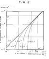
- the concentration of B is calculated from FIG.2.
- the abscissa is the mol ratio M B of B.
- the ordinate is the concentration of B in solid multiplied by 3/4.
- B is added into the floating crucible.
- 200g of GaAs is 13.83mol.
- a GaAs molecule consists of two atoms. Total number of mol is twice as much as the former value.
- the atomic weight of B is 10.81, if 123mg of B is doped into 200g of GaAs, the mol ratio of B is 4.11 X 10 -3 . Multiplying it by (3/4), we obtain 3.1 X 10 -3 for the abscissa variable ( 3N B / 4 ) . From FIG.2 the B concentration in crystal is
- the impurity concentrations of In and B are measured throughout the single crystal ingot. They were,
- the lattice misfit coefficients 8 were calculated at many sampling point from the measured impurity concentrations.
- the crystal ingot was two inches in diameter. The weight was 1.5 kg. The crystal grown was a single throughout. Specific resistivity was 5 to 10 X 10 7 ⁇ cm. It means the crystal is semi-insulating semiconductor.
- the ingot was sliced into many thin wafers. Wafers were etched. EPDs on wafers were counted. Except the peripheries with 5mm width, we obtained the average EPD
- EPD was very low. Especially it was a surprising result that EPD was so much low at the back end. We obtained a single crystal of very low dislocation density.
- a GaAs crystal doped with In, B and Si is grown along ⁇ 100 > direction by the LEC method.
- GaAs polycrystal B 2 0 3 , In and B are totally same with the last example.
- Si is newly doped by 225 mg. Si is added in the floating crucible, in which 200g of GaAs is charged.
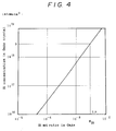
- FIG.4 shows the relationship between Si mol ratio in GaAs and Si concentration in a grown crystal.
- Si mol ratio is 2.9 X 10- 3 . From FIG.4, Si concentration in a GaAs host crystal turns out to be
- Bond lengths are :
- the abscissa is the B concentration x 1 .
- the ordinate is the In concentration x 2 .
- the region covered by many parallel slant lines is the region which satisfies the requirement of the invention (
- the region covered by double parallel slant lines is the region in which
- the doping concentration of anisoelectronic impurities should be determined by the desirable specific resistivity of the crystal.
- the double dopings of isoelectronic impurities can reduce the dislocation density without any influence over the electronic property.
Landscapes
- Chemical & Material Sciences (AREA)
- Engineering & Computer Science (AREA)
- Crystallography & Structural Chemistry (AREA)
- Materials Engineering (AREA)
- Metallurgy (AREA)
- Organic Chemistry (AREA)
- Inorganic Chemistry (AREA)
- Crystals, And After-Treatments Of Crystals (AREA)
- Liquid Deposition Of Substances Of Which Semiconductor Devices Are Composed (AREA)
Applications Claiming Priority (2)
| Application Number | Priority Date | Filing Date | Title |
|---|---|---|---|
| JP34560/84 | 1984-02-23 | ||
| JP59034560A JPS60176997A (ja) | 1984-02-23 | 1984-02-23 | 低転位密度の3−5化合物半導体単結晶 |
Publications (3)
| Publication Number | Publication Date |
|---|---|
| EP0153119A2 true EP0153119A2 (de) | 1985-08-28 |
| EP0153119A3 EP0153119A3 (en) | 1985-09-25 |
| EP0153119B1 EP0153119B1 (de) | 1987-05-13 |
Family
ID=12417695
Family Applications (1)
| Application Number | Title | Priority Date | Filing Date |
|---|---|---|---|
| EP85300889A Expired EP0153119B1 (de) | 1984-02-23 | 1985-02-11 | Einkristall einer III-V-Halbleiterverbindung mit kleiner Versetzungsdichte |
Country Status (5)
| Country | Link |
|---|---|
| US (1) | US4584174A (de) |
| EP (1) | EP0153119B1 (de) |
| JP (1) | JPS60176997A (de) |
| CA (1) | CA1239851A (de) |
| DE (1) | DE3560173D1 (de) |
Cited By (1)
| Publication number | Priority date | Publication date | Assignee | Title |
|---|---|---|---|---|
| GB2503525A (en) * | 2012-06-30 | 2014-01-01 | Timothy Lionel David Mccrea | Bicycle or wall-mounted helmet holder |
Families Citing this family (10)
| Publication number | Priority date | Publication date | Assignee | Title |
|---|---|---|---|---|
| JPS60260500A (ja) * | 1984-06-05 | 1985-12-23 | Sumitomo Electric Ind Ltd | 低転位密度のInP単結晶とその製造方法 |
| DE3508024A1 (de) * | 1985-03-07 | 1986-09-11 | Licentia Patent-Verwaltungs-Gmbh, 6000 Frankfurt | Halbleiteranordnung aus verbindungshalbleitermaterial |
| JPS62128999A (ja) * | 1985-11-25 | 1987-06-11 | Sumitomo Electric Ind Ltd | 2重るつぼを用いた単結晶引上方法及び2重るつぼ |
| JPS62256793A (ja) * | 1986-05-01 | 1987-11-09 | Shin Etsu Handotai Co Ltd | 化合物半導体単結晶の引上方法 |
| BE1005713A3 (fr) * | 1992-03-02 | 1993-12-28 | Solvay | Procede de stabilisation d'un hydrofluoroalcane et compositions comprenant au moins un hydrofluoroalcane. |
| US8134175B2 (en) * | 2005-01-11 | 2012-03-13 | Massachusetts Institute Of Technology | Nanocrystals including III-V semiconductors |
| WO2008133660A2 (en) | 2006-11-21 | 2008-11-06 | Qd Vision, Inc. | Nanocrystals including a group iiia element and a group va element, method, composition, device and other prodcucts |
| CN112176410A (zh) * | 2020-09-24 | 2021-01-05 | 中国电子科技集团公司第十一研究所 | 低掺N型锑化铟InSb晶体掺杂方法 |
| CN114808131B (zh) * | 2022-04-20 | 2023-05-09 | 北京通美晶体技术股份有限公司 | 一种GaAs单晶及其VGF制备方法 |
| DE102024202321A1 (de) | 2024-03-12 | 2025-09-18 | Forschungsverbund Berlin E.V. | Verbesserte dotierte InP-Kristalle |
Family Cites Families (9)
| Publication number | Priority date | Publication date | Assignee | Title |
|---|---|---|---|---|
| US2858275A (en) * | 1954-12-23 | 1958-10-28 | Siemens Ag | Mixed-crystal semiconductor devices |
| DE1188555B (de) * | 1960-05-10 | 1965-03-11 | Wacker Chemie Gmbh | Verfahren zur Herstellung hochreiner kristalliner Koerper aus Nitriden, Phosphiden oder Arseniden der III. Hauptgruppe des Periodensystems |
| US3496118A (en) * | 1966-04-19 | 1970-02-17 | Bell & Howell Co | Iiib-vb compounds |
| US4404265A (en) * | 1969-10-01 | 1983-09-13 | Rockwell International Corporation | Epitaxial composite and method of making |
| US3932883A (en) * | 1972-08-08 | 1976-01-13 | The British Secretary of State for Defense | Photocathodes |
| FR2296264A1 (fr) * | 1974-12-24 | 1976-07-23 | Radiotechnique Compelec | Procede de realisation de dispositif semi-conducteur a heterojonction |
| JPS581539B2 (ja) * | 1978-07-07 | 1983-01-11 | 三菱化成ポリテック株式会社 | エピタキシヤルウエハ− |
| US4213801A (en) * | 1979-03-26 | 1980-07-22 | Bell Telephone Laboratories, Incorporated | Ohmic contact of N-GaAs to electrical conductive substrates by controlled growth of N-GaAs polycrystalline layers |
| US4399097A (en) * | 1981-07-29 | 1983-08-16 | Bell Telephone Laboratories, Incorporated | Preparation of III-V materials by reduction |
-
1984
- 1984-02-23 JP JP59034560A patent/JPS60176997A/ja active Granted
-
1985
- 1985-02-11 EP EP85300889A patent/EP0153119B1/de not_active Expired
- 1985-02-11 DE DE8585300889T patent/DE3560173D1/de not_active Expired
- 1985-02-21 CA CA000474879A patent/CA1239851A/en not_active Expired
- 1985-02-21 US US06/704,027 patent/US4584174A/en not_active Expired - Lifetime
Cited By (1)
| Publication number | Priority date | Publication date | Assignee | Title |
|---|---|---|---|---|
| GB2503525A (en) * | 2012-06-30 | 2014-01-01 | Timothy Lionel David Mccrea | Bicycle or wall-mounted helmet holder |
Also Published As
| Publication number | Publication date |
|---|---|
| EP0153119B1 (de) | 1987-05-13 |
| JPH0254319B2 (de) | 1990-11-21 |
| DE3560173D1 (en) | 1987-06-19 |
| CA1239851A (en) | 1988-08-02 |
| JPS60176997A (ja) | 1985-09-11 |
| EP0153119A3 (en) | 1985-09-25 |
| US4584174A (en) | 1986-04-22 |
Similar Documents
| Publication | Publication Date | Title |
|---|---|---|
| EP0160373B1 (de) | Einkristall einer III-V-Halbleiterverbindung mit niedriger Versetzungsdichte | |
| US4478675A (en) | Method of producing GaAs single crystals doped with boron | |
| EP0153119B1 (de) | Einkristall einer III-V-Halbleiterverbindung mit kleiner Versetzungsdichte | |
| EP0149898B1 (de) | LEC-Verfahren und Vorrichtung zur Herstellung eines Einkristalls halbleitender Verbindungen | |
| EP0149082B1 (de) | Galliumarsenid-Einkristall und seine Herstellung | |
| US4594173A (en) | Indium doped gallium arsenide crystals and method of preparation | |
| US4196171A (en) | Apparatus for making a single crystal of III-V compound semiconductive material | |
| Cockayne et al. | The growth and perfection of single crystal indium phosphide produced by the LEC technique | |
| Henry et al. | InP growth and properties | |
| US5728212A (en) | Method of preparing compound semiconductor crystal | |
| JP3797824B2 (ja) | p型GaAs単結晶およびその製造方法 | |
| JP4235711B2 (ja) | 縦型ボート法によるGaAs単結晶の製造方法 | |
| Clemans et al. | Bulk III‐V Compound Semi‐Conductor Crystal Growth | |
| EP0206514B1 (de) | Doppeltiegel zum Ziehen von Einkristallen | |
| JP3931956B2 (ja) | シリコン単結晶の育成方法 | |
| GB2189166A (en) | A single crystal of IIIb-Vb compound, particularly GaAs, and method for producing the same | |
| JPH08758B2 (ja) | クロムドープ半絶縁性ガリウム・ヒ素単結晶の製造方法 | |
| Coquille et al. | Growth of low-dislocation semi-insulating InP (Fe, Ga) | |
| Fujii et al. | Growth cells of heavily In-doped LEC GaAs crystals | |
| JP3451658B2 (ja) | 混晶半導体単結晶の成長方法 | |
| Hirano et al. | Crystal growth of low EPD S-doped< 100> InP by facet formation | |
| KR950003430B1 (ko) | 더블-도우핑(double-doping)에 의한 p-type GaAs 단결정 성장방법 | |
| JPS61247700A (ja) | 3−5族化合物半導体の製造方法 | |
| JPS57170899A (en) | Manufacture of ggg single crystal | |
| JPS6389497A (ja) | 珪素添加ガリウム砒素単結晶の製造方法 |
Legal Events
| Date | Code | Title | Description |
|---|---|---|---|
| PUAI | Public reference made under article 153(3) epc to a published international application that has entered the european phase |
Free format text: ORIGINAL CODE: 0009012 |
|
| PUAL | Search report despatched |
Free format text: ORIGINAL CODE: 0009013 |
|
| AK | Designated contracting states |
Designated state(s): DE FR GB IT NL SE |
|
| AK | Designated contracting states |
Designated state(s): DE FR GB IT NL SE |
|
| 17P | Request for examination filed |
Effective date: 19850821 |
|
| 17Q | First examination report despatched |
Effective date: 19860626 |
|
| GRAA | (expected) grant |
Free format text: ORIGINAL CODE: 0009210 |
|
| AK | Designated contracting states |
Kind code of ref document: B1 Designated state(s): DE FR GB IT NL SE |
|
| ITF | It: translation for a ep patent filed | ||
| REF | Corresponds to: |
Ref document number: 3560173 Country of ref document: DE Date of ref document: 19870619 |
|
| ET | Fr: translation filed | ||
| PLBE | No opposition filed within time limit |
Free format text: ORIGINAL CODE: 0009261 |
|
| STAA | Information on the status of an ep patent application or granted ep patent |
Free format text: STATUS: NO OPPOSITION FILED WITHIN TIME LIMIT |
|
| 26N | No opposition filed | ||
| ITTA | It: last paid annual fee | ||
| EAL | Se: european patent in force in sweden |
Ref document number: 85300889.4 |
|
| REG | Reference to a national code |
Ref country code: GB Ref legal event code: 746 Effective date: 19970121 |
|
| ITPR | It: changes in ownership of a european patent |
Owner name: OFFERTA DI LICENZA AL PUBBLICO |
|
| REG | Reference to a national code |
Ref country code: FR Ref legal event code: D6 |
|
| PGFP | Annual fee paid to national office [announced via postgrant information from national office to epo] |
Ref country code: DE Payment date: 20010205 Year of fee payment: 17 |
|
| PGFP | Annual fee paid to national office [announced via postgrant information from national office to epo] |
Ref country code: SE Payment date: 20010206 Year of fee payment: 17 |
|
| PGFP | Annual fee paid to national office [announced via postgrant information from national office to epo] |
Ref country code: GB Payment date: 20010207 Year of fee payment: 17 |
|
| PGFP | Annual fee paid to national office [announced via postgrant information from national office to epo] |
Ref country code: FR Payment date: 20010213 Year of fee payment: 17 |
|
| PGFP | Annual fee paid to national office [announced via postgrant information from national office to epo] |
Ref country code: NL Payment date: 20010228 Year of fee payment: 17 |
|
| REG | Reference to a national code |
Ref country code: GB Ref legal event code: IF02 |
|
| PG25 | Lapsed in a contracting state [announced via postgrant information from national office to epo] |
Ref country code: GB Free format text: LAPSE BECAUSE OF NON-PAYMENT OF DUE FEES Effective date: 20020211 |
|
| PG25 | Lapsed in a contracting state [announced via postgrant information from national office to epo] |
Ref country code: SE Free format text: LAPSE BECAUSE OF NON-PAYMENT OF DUE FEES Effective date: 20020212 |
|
| PG25 | Lapsed in a contracting state [announced via postgrant information from national office to epo] |
Ref country code: NL Free format text: LAPSE BECAUSE OF NON-PAYMENT OF DUE FEES Effective date: 20020901 |
|
| PG25 | Lapsed in a contracting state [announced via postgrant information from national office to epo] |
Ref country code: DE Free format text: LAPSE BECAUSE OF NON-PAYMENT OF DUE FEES Effective date: 20020903 |
|
| EUG | Se: european patent has lapsed |
Ref document number: 85300889.4 |
|
| GBPC | Gb: european patent ceased through non-payment of renewal fee |
Effective date: 20020211 |
|
| PG25 | Lapsed in a contracting state [announced via postgrant information from national office to epo] |
Ref country code: FR Free format text: LAPSE BECAUSE OF NON-PAYMENT OF DUE FEES Effective date: 20021031 |
|
| NLV4 | Nl: lapsed or anulled due to non-payment of the annual fee |
Effective date: 20020901 |
|
| REG | Reference to a national code |
Ref country code: FR Ref legal event code: ST |