EP0137594B1 - Adressenübersetzungsspeicher - Google Patents
Adressenübersetzungsspeicher Download PDFInfo
- Publication number
- EP0137594B1 EP0137594B1 EP84304787A EP84304787A EP0137594B1 EP 0137594 B1 EP0137594 B1 EP 0137594B1 EP 84304787 A EP84304787 A EP 84304787A EP 84304787 A EP84304787 A EP 84304787A EP 0137594 B1 EP0137594 B1 EP 0137594B1
- Authority
- EP
- European Patent Office
- Prior art keywords
- row
- cells
- addressable memory
- rows
- content addressable
- Prior art date
- Legal status (The legal status is an assumption and is not a legal conclusion. Google has not performed a legal analysis and makes no representation as to the accuracy of the status listed.)
- Expired - Lifetime
Links
Images


Classifications
-
- G—PHYSICS
- G11—INFORMATION STORAGE
- G11C—STATIC STORES
- G11C15/00—Digital stores in which information comprising one or more characteristic parts is written into the store and in which information is read-out by searching for one or more of these characteristic parts, i.e. associative or content-addressed stores
- G11C15/04—Digital stores in which information comprising one or more characteristic parts is written into the store and in which information is read-out by searching for one or more of these characteristic parts, i.e. associative or content-addressed stores using semiconductor elements
Definitions
- the present invention generally relates to systems for translating virtual memory addresses into physical memory addresses, and more particularly to a new and improved content addressable memory (CAM) cell useful in such systems.
- CAM content addressable memory
- a content addressable memory is a memory device in which all memory cells are selected by contents rather than by addresses, which is also known as an associative memory.
- Another related object of this invention is to provide a shiftable content addressable memory device that obviates address decode circuitry.
- US Patent Specification No. 4 296 475 discloses an associative memory which can provide a data word output in response to input of a key word into a plurality of word rows.
- Siemens-System 4004, Gottfeld 4004/151-2, Cardio und Betationsliste published by Siemens AG July 1974 discloses an associative store having a content addressable memory of eight word rows. During an updating operation the content of the 8th row is lost and the content of the first 7 rows is displaced into rows 2 to 8. This releases the first row to receive a new word entry.
- US-A-3 938 100 is directed to addressing apparatus in which addresses are sequentially examined using a sequence in which the most heavily used addresses are examined first.
- a virtual address register is used to receive the virtual address which is then supplied to a virtual address fan-out circuit and a virtual address comparison circuit.
- the latter circuit compares the virtual address with the associative words associated with each of the associative registers. If a correspondence occurs an absolute address select circuit provides a signal for selecting the absolute address with an absolute page identifier from a circuit and a signal from a match fan-out circuit via a match fan-in circuit and match register.
- US-A-3 938 100 uses a large number of circuit means, i.e. the virtual address register, virtual address fan-out circuit, virtual address comparison circuit, etc. for searching the matching address.
- the present invention uses a simpler searching system based on CAM cells.
- an address translation buffer for receiving a virtual address and providing an output match signal, said buffer comprising: P rows by N columns of content addressable memory cells (CAM1 to CAMp) for storing a virtual address in each row, wherein P and N are integers greater than one; means (Q1-1 to Q1-m) for sequentially interconnecting the content addressable memory cells in each respective column so that the content of each content addressable memory cell (e.g. CAM2) can be shifted to the next lower row (e.g.
- CAM3 in accordance with an established hierachy of highest (CAM1) to lowest (CAMp) priority of said rows of content addressable memory cells; means (10) for inputting said virtual address to each row of content addressable memory cells for comparison with the content of each row of content addressable memory cells to determine if a match occurs; characterised by P rows of RAM cells (RAM1 to RAMp) for storing in each row a physical address corresponding to the virtual address stored in the corresponding row of content addressable memory cells, means (Q2-1 to Q2-m) for sequentially interconnecting the RAM cells so that the content of each RAM cell (e.g. RAM2) can be shifted to the next lower row (e.g.
- RAM3 in accordance with an established hierachy of highest (RAM1) to lowest (RAMp) priority of said rows of RAM cells and means (CTL1 to CTLp, CMUX, RMUX) for controlling the shifting between said rows of content addressable memory cells and RAM cells arranged so that, after receipt of a virtual address that matches the content of one of said rows of content addressable memory cells, the contents of the higher priority rows of content addressable memory cells and RAM cells are shuffled down to the respective next lower priority rows and said content of said one row of content addressable memory cells and of the corresponding row of RAM cells is written into the highest priority row of said rows of content addressable memory cells and RAM cells.
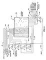
- a memory address bus 10 transmitting memory addresses from a processor 11 is coupled to the A input terminals of a multiplexer 12 and to input terminals of an address translation buffer 14.
- the address translation buffer (ATB) 14 is divided into three basic parts, which will be explained in greater detail hereinafter.
- a first part is a stack of rows of memory cells forming a content addressable memory (CAM), which is disposed for storing virtual addresses.
- a second part is a stack (equal in size to the CAM stack) of rows of memory cells forming a random access memory (RAM), which is disposed for storing physical addresses corresponding to the virtual addresses.
- CAM content addressable memory
- RAM random access memory
- the third part of the ATB 14 is a stack of an equal number of control circuits disposed for controlling read-in, readout or shifting operations to be explained hereafter.
- the output terminals of the multiplexer 12 are coupled to a memory fabric 15 by means of a bus 16. It is the function of the memory address translation buffer 14 to translate virtual memory addresses into physical addresses, and the output terminals thereof are coupled to the B input terminals of the multiplexer 12 on a bus 17.
- the multiplexer 12 selects between either the A or the B input terminals by means of a control signal supplied on a line 18 from the processor 11.
- the address translation buffer 14 is controlled by a control state machine 19 which is disposed for transmitting control signals to and from the buffer on lines 20. Control signals from the processor 11 are transmitted to the control state machine 19 on lines 22. Additional input and output signals to and from the address translation buffer 14, which will be more fully understood following the description hereinbelow, are the address translation buffer RAM data (i.e., ATB RAM DATA) supplied on a bus 24, and the contents of the last row of cells (i.e., LAST ROW) within the buffer 14 supplied from the processor 11 on a bus 26 to the processor.
- ATB RAM DATA address translation buffer RAM data supplied on a bus 24
- LAST ROW the contents of the last row of cells
- buses 10, 24 and 26 may be a single bus that is time shared by operation in a conventional manner. These buses are illustrated separately for explanation purposes only.
- Physical addresses are loaded into the RAM portion of the ATB 14 on the bus 24, while corresponding virtual addresses are loaded into the CAM portion of the ATB by means of the bus 10.
- a comparison operation is performed within the CAM portion of the ATB 14 to locate a physical address stored in the RAM portion of the ATB.
- the physical address if found, is supplied on the output bus 17 to the B input terminals of the multiplexer 12; and, from there to the memory fabric 15 on the bus 16 when the control signal on the line 18 is active. If no comparison match is found, then the ENTRY NOT PRESENT signal is supplied back to the processor 11 on the line 28.
- FIG. 2 a block diagram of the address translation buffer 14 is illustrated.
- the memory address supplied on the bus 10 is applied to the B input terminals of a multiplexer referred to herein as CMUX 30.
- the output of the CMUX 30 is supplied on a bus 31 to the first row of the p rows of CAM cells (CAM 1) of a memory 32.
- the output of the last (p) row of CAM cells (CAM p) is coupled to an output bus 26a of the bus 26, and is also coupled back to the A input terminals of the CMUX 30.
- the CMUX 30 routes the signals on either the A or the B input terminals to the CAM 1 as a function of a SHUFFLE ALL control signal supplied on a line 20d of the lines 20.
- the ATB RAM DATA bus 24 is coupled to the A input terminals of a multiplexer referred to herein as RMUX 34.
- the output of the RMUX is supplied on a bus 38 to the first row of p rows of RAM cells (RAM 1) of a memory 35. Outputs of each of the rows of RAM cells 1 through p are coupled to the bus 17, which is coupled back to the B input terminals of the RMUX 34.
- the output of the last (p) row of RAM cells (CAM p) is supplied on a bus 26b of the bus 26 for purposes to be described hereinafter.
- the RMUX 34 routes the signals on either the A or the B input terminals as a function of a LOAD RAM control signal supplied on a line 20e of the lines 20.
- the shifting of the contents of the CAM cells 32 row by row down the stack, or the RAM cells 35 row by row down the stack, is controlled by a stack of p control circuits 37.
- Each of the control circuits 37 is coupled to respective ones of the rows of CAM and RAM cells.
- the control lines 20 from the control state machine 19 are provided as inputs to the stack of p control circuits 37, which will be explained in greater detail hereinafter.
- the output of the last, that is the pth control circuit provides the ENTRY NOT PRESENT signal on the line 28.
- the memory 32 contains p virtual addresses each being stored in a different row thereof.
- the memory 35 contains p physical addresses each being stored in a different row thereof, which correspond to each of the virtual addresses stored in corresponding rows of the memory 32.
- a virtual address is translated into a physical address by means of the searching scheme of each of the individual rows of CAM cells 1 through p to thereby find a matching address, and the contents of the corresponding row of RAM cells are read out as the actual or physical address. Moreover, by continuously writing the accessed row of cells into the top row and shifting the other rows down, the last row of cells will thus contain the least recently used addresses.
- a control matrix 40 has an address portion 40a and a readout portion 40b.
- the ENTRY NOT PRESENT signal supplied on the line 28 from the buffer 14 is coupled to a first column of the address portion 40a.
- Three additional signals of the control signals supplied on lines 20a and 20b of the lines 20 and 26' of the bus 26, which are referred to herein as ALL VALID, ALL LOCKED, and LAST UNLOCKED, respectively, are coupled to the next three address inputs of the address portion 40a.
- An ATB OPERATION control signal is supplied on a line 22a of the lines 22 to the data D input terminal of a flip-flop 42.
- the output of this flip-flop is coupled to one of the address input terminals of the address portion 40a.
- An ATB SELECT OPERATION control signal is supplied on a line 22b of the control signal lines 22 to the data D input terminal of another flip-flop 44, which has the Q output thereof coupled to yet another address input terminal of the address portion 40a.
- Two output lines of the readout portion 40b, which are supplied on lines 45 and 46, are coupled to the data D input terminals of flip-flops 47 and 48, respectively.
- the Q output terminals of the flip-flops 47 and 48 are coupled to the last two address input terminals of the address portion 40a.
- the control signals supplied on the lines 20 are provided at the output terminals of the readout portion 40b of the control matrix 40. These signals are referred to herein as SHUFFLE, SHUFFLE ALL, LOAD RAM, ATB RESULT, and ATB ERROR, and are supplied on lines 20c, 20d, 20e, 22c and 22d, respectively.
- a final output signal SHUFFLE-TO-INVALID is provided from the Q output terminal of a flip-flop 50 on a line 20f, which has the data D input thereof coupled to an output terminal of the readout portion 40b.
- the reset (R) input terminals of the flip-flops 42, 44, 47, 48 and 50 are coupled to a line 22e transmitting a RESET signal from the processor 11.
- the numbers in the same row are read out from the readout portion.
- the output would be as follows: a high level signal on the line 20c (SHUFFLE), a high level signal on the line 20e (LOAD RAM), and a high level signal on the line 22c (ATB RESULT).
- SHUFFLE high level signal on the line 20c
- LOAD RAM high level signal on the line 20e
- ATB RESULT high level signal on the line 22c
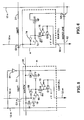
- the memory address supplied on the bus 10 from the processor 11 is coupled to the CAM 3 cells 1 through m.
- the virtual address to be stored in the CAM 3 is supplied on lines 50 to drain terminals of transistors Q1-1 through Q1-m.
- the lines 50 would be the same as the bus 31 from the CMUX 30.
- the source terminals of the transistors Q1-1 through Q1-m are coupled to inputs of the CAM cells 1 through m.
- the gate terminals of these transistors are coupled to a line 51, which transmits a SHIFT signal provided by a control circuit CTL 3.
- MOS and CMOS transistors are typically fabricated symmetrical.
- a high level voltage is +5 volts and a low level voltage is ground potential (zero volts).
- the reference numerals used for the transistors shown relate to only the illustrated row of memory cells (i.e., row 3), and it being understood that the other rows (not shown) also have transistors configured in the same way as that illustrated in FIG. 4.
- the memory address supplied on the bus 10 to the CAM 3 is the address to be compared with the contents of the CAM cells 1 through m of row 3.
- the contents of the CAM cells 1 through m are loaded by means of the lines 50 in response to a SHIFT signal.
- the contents of the CAM cells 1 through m in the CAM 3 are supplied to the next row of CAM cells by means of lines 52-1 through 52-m.
- a MATCH signal is supplied on a line 54 to the control circuit CTL 3 from the CAM 3.
- the contents of the RAM cells in the stack 35 are transmitted from the previous row to row 3 by means of lines 56, which lines are coupled to the drain terminals of transistors Q2-1 through Q2-n.
- the lines 50 would be the same as the bus 38 from the RMUX 34.
- the source terminals of the transistors Q2-1 through Q2-n are coupled to the RAM cells 1 through n of the RAM 3.
- the gate terminals of these transistors are also coupled to the SHIFT line 51.
- the RAM cells 1 and 2 of the RAM 3 have an additional function to be explained further hereinafter, and accordingly, transistors Q3-1 and Q3-2 are coupled between the inputs to the RAM cells 1 and 2, respectively, and ground potential.
- the gate terminals of the transistors Q3-1 and Q3-2 are coupled to the RESET signal line 22e. Hence, when the RESET signal is at a high level, the transistors Q3-1 and Q3-2 are turned on thereby grounding the inputs to the RAM cells 1 and 2, which sets a zero in these cells.
- the output or contents of the RAM 3 cells are transmitted to the next row by means of lines 60-1 through 60-n.
- the line 60-1 is coupled to an input terminal of the control circuit CTL 3 and is also identified as VALID.
- the line 60-2 is also coupled to an input terminal of the control circuit CTL 3 and is also identified herein as UNLOCKED.
- the RESET signal going high forces a low-level signal on the lines 60-1 and 60-2, which causes the UNLOCKED and VALID signals to go low.
- the content readout of the RAM cells in the RAM 3 row is provided at the drain terminals of transistors Q4-1 through Q4-n.
- the source terminals of the transistors Q4-1 through Q4-n are coupled to the bus 17, which transmits the address output to the MUX 12 (FIG. 1).
- the gate terminals of the transistors Q4-1 through Q4-n are coupled to a word line 62 from the control circuit CTL 3.
- the memory address supplied on the bus 10 is simultaneously supplied to all of the CAM cells CAM 1 through CAM p of the memory 32 and if this address matches an address stored in any one of the rows of the CAM cells, a MATCH signal is supplied on the line 54 to a control circuit such as CTL 3.
- the word line 62 is raised to a high level thereby coupling the contents of the RAM cells 1 through n out to the bus 17.
- the MATCH signal line 54 is coupled to the drain terminal of the transistor Q6 and to the drain terminal of another transistor Q8.
- the source terminal of the transistor Q6 is coupled to the drain terminal of another transistor Q10 and the source terminal thereof is coupled to ground potential.
- the transistors Q6 and Q10 form an open drain NAND gate.
- the output terminal of the inverter 64 is coupled to the gate terminal of the transistor Q8.
- the source terminal of the transistor Q8 is coupled to the drain terminal of yet another transistor Q12 having the drain terminal thereof coupled to ground potential.
- the transistors Q8 and Q12 also form an open drain NAND gate.
- a line 50-m of the lines 50 which transmits load data from the previous row CAM cell, is coupled to the drain terminal of a transistor Q1-m and the source terminal thereof is coupled to the gate terminal of the transistor Q10, the input of an inverter 66, and to the output of yet another inverter 68.
- the gate terminal of the transistor Q1-m is coupled to the SHIFT line 51.
- the inverters 66 and 68 form a latch circuit, wherein the inverter 68 is scaled smaller than the inverter 66 so as to enable the load data from the prior row to override the inverter 68 when changing the state of the CAM cell.
- the output of the inverter 66 is coupled to the gate terminal of the transistor Q12 and to the input of the feedback inverter 68.
- the output of the feedback inverter 68 is coupled back to the input of the inverter 66, thereby forming the latch circuit.
- the output of the inverter 66 is coupled to the drain terminal of a transistor Q14 having a gate terminal thereof coupled to a ⁇ 2 clock input signal.
- clock signals ⁇ 1 and ⁇ 2 discussed herein, and each is complementary to the other and they are non-overlapping. These clock signals are generated in a well-known manner not shown herein.
- the source terminal of the transistor Q14 is coupled to the input of an inverter 70 and to the drain terminal of a p-channel transistor Q16 having the drain terminal thereof coupled to a source of positive voltage (+ V).
- the output of the inverter 70 is the output of the CAM cell m and is coupled to a line 52m of the bus 52. Also, the output of the inverter 70 is coupled to the gate terminal of the p-channel transistor Q16. It is noted that when the transistor Q16 is a p-channel transistor, all other transistors would be n-channel. However, a reverse in polarity of the various transistors described herein could be made without departing from the spirit of the invention.
- the output of the inverter 66 is at a high or a low level depending upon the state of the CAM cell m. Assume, for example, that the output of the inverter 66 is at a high level which would turn on the transistor Q12. If the state of the line 10-m is also at a high level (which would mean that for purposes of an individual cell there would be a match), the output of the inverter 64 would be at a low level thereby turning off the transistor Q8. Similarly, the transistor Q6 would be turned on; however, the transistor Q10 would be turned off since the output of the inverter 68 is opposite to the output of the inverter 66 (i.e., a low level). Accordingly, the MATCH signal line 54 remains at a high level since the line 54 is biased at a preselected voltage level in a conventional well-known manner.
- the SHIFT signal line 51 is raised to a high level and the state of the line 50-m (i.e., the state of the corresponding cell in the previous row) would be transmitted to the input of the inverter 66.
- the state of the line 50-m is at a high level.
- this high-level signal is applied to the input of the inverter 66 when SHIFT is high, thereby dropping the output of this inverter to a low level.
- This low-level signal is coupled back through the inverter 68 to a high level, which locks the cell m in a one state.
- the state of the inverter 70-transistor Q16 buffer circuit will be changed according to the state of the latch circuit (inverters 66 and 68).
- FIG. 6 illustrates in greater detail an individual RAM cell such as RAM cell n.
- the state of the previous RAM cell is present on the line 56-n of the lines 56 and is coupled through the transistor Q2-n when a SHIFT signal is high on the line 51.
- This state is applied to the input of an inverter 72 and the output thereof is coupled to the input of yet another feedback inverter 74, to the gate terminal of a transistor Q20 and to the drain terminal of a transistor Q22.
- the gate terminal of the transistor Q22 is coupled to the ⁇ 2 clock signal line.
- the inverter 74 is scaled smaller than the inverter 72, and these inverters form a latch circuit.
- the gate terminal of the transistor Q4-n is coupled to the word line 62 and the drain terminal thereof is coupled to line 17-n of the bus 17 as was illustrated in FIG. 4 and described hereinabove.
- the source terminal of the transistor Q4-n is coupled to the drain terminal of the transistor Q20 and the source terminal thereof is coupled to ground potential.
- the transistors Q20 and Q4-n form an open drain NAND gate.
- the source terminal of the transistor Q22 is coupled to the input terminal of an inverter 76 and the output thereof is coupled to the gate terminal of a p-channel transistor Q24 having the drain terminal thereof coupled to a voltage source (+ V).
- the source terminal of Q24 is coupled back to the input terminal of the inverter 76.
- the output of the inverter 76 is also coupled to the line 60-n, which line is coupled to the next row of RAM cells as was illustrated in FIG. 4 and described hereinabove.
- the inverter 76 and the transistor Q24 form a buffer circuit.
- the transistor Q4-n is turned on and if the transistor Q20 is on, the line 17-n is pulled down to ground potential.
- the transistor Q20 would be turned on in response to a high-level signal at the output of the inverter 72, which indicates that the RAM cell is in a one state.
- the transistor Q20 is turned off and the line 17-n remains at its biased level.
- Each of the lines 17 are biased at a preselected voltage level in a conventional well-known manner.
- the MATCH signal line 54 is coupled to the drain terminal of a transistor Q30 and the source terminal thereof is coupled to the A input terminal of a multiplexer 80, to the gate terminal of another transistor Q32 and to the word line 62.
- the gate terminal of the transistor Q30 is coupled to the ⁇ 2 clock signal.
- the drain terminal of the transistor Q32 is coupled to the ENTRY NOT PRESENT signal line 28 and the source terminal thereof is coupled to ground potential.
- the VALID signal line 60-1 is coupled to the input terminal of an inverter 82 and the output of the inverter 82 is coupled to the B input terminal of the multiplexer 80 and to the gate terminal of a transistor Q34.
- the drain terminal of the transistor Q34 is coupled to the ALL VALID signal line 22a and the source terminal thereof is coupled to ground potential.
- the ENTRY NOT PRESENT, ALL LOCKED and the ALL VALID signal lines are biased at a preselected voltage level in a conventional well-known manner.
- the SHUFFLE-TO-INVALID signal line 20f is coupled to the SELECT input terminal of the multiplexer 80 and the output terminal of the multiplexer 80 is coupled to an inverting input terminal of an AND gate 84. When the SHUFFLE-TO-INVALID signal is at a high level, the B input terminal is selected and when at a low level, the A input terminal of the multiplexer 80 is selected.
- a CHAIN signal which is used in a shuffle-to-match and shuffle-to-invalid operations to be described further hereafter, is supplied on a line 86 to a first of two input terminals of an OR gate 88 and to the second input terminal of the AND gate 84.
- the output of the AND gate 84 couples the CHAIN signal to the next row control circuit.
- the SHUFFLE-ALL signal supplied on the line 20b is coupled to the second input terminal of the inverter 88, and the output terminal of the inverter 88 is coupled to one of two input terminals of an AND gate 90.
- the SHUFFLE signal supplied on the line 20c and the ⁇ 1 clock signal are applied to the two input terminals of an AND gate 92 and the output terminal of this AND gate is coupled to the second input terminal of the AND gate 90, which output terminal is also disposed for connection in the subsequent row control circuit.
- the output terminal of the AND gate 90 is coupled to the line 51 transmitting the SHIFT signal as described hereinabove.
- the ⁇ 1 clock signal forms part of the SHIFT signal, while the actual transfer of data from the prior row is controlled by the ⁇ 2 clock signal (FIG. 5 Q14 and FIG. 6 Q22). This arrangement assures stability of operation.
- the UNLOCKED signal supplied on the line 60-2 is coupled to the gate terminal of a transistor Q36 having the drain terminal thereof coupled to the ALL LOCKED signal line 22b and the source terminal thereof coupled to ground potential.
- FIGs. 2, 3 and 7 for aid in explaining the various shuffle operations.
- a matching virtual address is located in the CAM 3 row of cells.
- the MATCH signal supplied on the line 54 to the control circuit CTL 3 the contents of the RAM 3 row of cells is read out on the bus 17 and simultaneously loaded into the RAM 1 row of cells. It is therefore necessary to perform a shuffle-to-match operation.
- the information that was in the first row of cells is loaded into the second row of cells while the information that was in the second row of cells is loaded into the third row of cells.
- the AND gate 90 In order to perform the shuffle-to-match operation, it is necessary to enable the AND gate 90 by enabling the OR gate 88 and the AND gate 92.
- the CHAIN signal line In the first row control circuit CTL 1, the CHAIN signal line is tied to a high level voltage.
- a MATCH signal on the line 54 produces a high-level signal on the WORD LINE 62 when the ⁇ 2 clock signal is high, which also appears at the A input terminal of the multiplexer 80.
- the ENTRY NOT PRESENT signal line is pulled down to ground potential by the transistor Q32.
- the SHUFFLE-TO-INVALID signal line 20f is at a low level for all operations except where performing a LOAD ATB operation in which there is no match and in which an INVALID entry is present in the ATB. Accordingly, the high-level signal at the A input terminal of the multiplexer 80 is provided at the output terminal thereof and causes the AND gate 84 to be disabled. Hence, the CHAIN signal is not passed on to the fourth row of CAM and RAM cells, but was coupled between the first three rows for enabling the AND gate 90 thereby providing the SHIFT signal.
- the RAM CELLs 1 and 2 are reset to zero in response to a RESET signal on the line 22e.
- the RAM CELL 1 is set to a one thereby indicating a valid address is stored in that row. If, on the other hand, nothing has been loaded into a row of CAM and RAM cells, or data that has been loaded into a row of memory cells that has been explicitly denoted as invalid, the RAM CELL 1 will be set to zero, then the VALID line 60-1 will be at a low level.
- the output of the inverter 82 (FIG. 7) would be at a high level and if the SHUFFLE-TO-INVALID signal on the line 20f is at a high level, then the output of the inverter 82 is passed through the multiplexer 80 to disable the AND gate 84. For the next row of cells, the CHAIN signal is blocked. Hence, a shuffle operation is performed through the row having the invalid address.
- the least recently used address gravitates to the last row by virtue of each accessed address being relocated to the first row, while shuffling all other stored addresses down one row. If it is necessary to store another virtual-physical address pair, and there is no more space in the ATB, a decision is to be made by the processor 11 as to whether or not to erase the least recently used address in the last row of cells. To assist in this operation, a virtual-physical address pair may be assigned a locked status bit which would prevent erasure. This status bit is stored in the RAM CELL 2 and the signal on this CELL's output line 60-2 is referred to herein as UNLOCKED.
- the address pair stored in the last (pth) row of cells is either an INVALID or a LOCKED address, then it is automatically cycled (during an idle time period) up to the first row and all rows are shuffled down one row by use of the SHUFFLE ALL signal.
Landscapes
- Static Random-Access Memory (AREA)
Claims (3)
- Adressenübersetzungsspeicher zur Eingabe einer virtuellen Adresse und zur Ausgabe eines Übereinstimmungssignals mit:
P Reihen und N Spalten von inhaltsadressierbaren Speicherzellen (CAM1 bis CAMp) zur Speicherung einer virtuellen Adresse in jeder Reihe, wobei P und N ganze Zahlen größer als 1 sind;
Einrichtungen (Q1-1 bis Q1-m) zur sequentiellen Verbindung der inhaltsadressierbaren Speicherzellen in jeder entsprechenden Spalte, so daß der Inhalt jeder inhaltsadressierbaren Speicherzelle (z.B. CAM2) zur nächst niedrigeren Reihe (z.B. CAM3) verschoben werden kann, und zwar gemäß einer festgesetzten Hierarchie von höchster (CAM1) zu niedrigster (CAMp) Priorität der Reihen von inhaltsadressierbaren Speicherzellen;
Einrichtungen (10) zur Eingabe der virtuellen Adressen in jede Reihe der inhaltsadressierbaren Speicherzellen zum Vergleich mit dem Inhalt jeder Reihe von inhaltsadressierbaren Speicherzellen zur Feststellung des Auftretens einer Übereinstimmung;
gekennzeichnet durch P Reihen von RAM Zellen (RAM1 bis RAMp) zur Speicherung einer physikalischen Adresse in jeder Reihe entsprechend der in der entsprechenden Reihe der inhaltsadressierbaren Speicherzellen gespeicherten virtuellen Adresse,
Einrichtungen (Q2-1 bis Q2-m) zur sequentiellen Verbindung der RAM Zellen in der Weise, daß der Inhalt jeder RAM Zelle (z.B. RAM2) zur nächst niedrigeren Reihe (z.B. RAM3) gemäß einer festgesetzten Hierarchie von einer höchsten (RAM1) zu einer niedrigsten (RAMp) Priorität der Reihen von RAM Zellen verschoben werden kann und Einrichtungen (CTL1 bis CTLp, CMUX, RMUX) zur Steuerung der Verschiebung zwischen den Reihen inhaltsadressierbarer Speicherzellen und RAM Zellen, die so angeordnet sind, daß nach Erhalt einer virtuellen Adresse, die mit dem Inhalt einer der Reihen inhaltsadressierbarer Speicherzellen übereinstimmt, die Inhalte der Reihen der inhaltsadressierbaren Speicherzellen mit höherer Priorität und der RAM Zellen nach unten zu den Reihen mit der entsprechenden nächst niedrigeren Priorität verschoben werden und der Inhalt der einen Reihe der inhaltsadressierbaren Speicherzellen und der entsprechenden Reihe von RAM Zellen in diejenige Reihe inhaltsadressierbarer Speicherzellen und RAM Zellen eingeschrieben wird, die die höchste Priorität aufweist. - Adressenübersetzungsspeicher nach Anspruch 1, dadurch gekennzeichnet, daß jede inhaltsadressierbare Speicherzelle aufweist:
eine Speicherschaltung (66, 68) zur Speicherung eines Datenbits mit einem Ausgangsanschluß "nicht wahr" und einem Ausgangsanschluß "wahr";
erste Einrichtungen (54, Q6 und Q12), die zwischen einen Ausgangsanschluß für übereinstimmende Daten und ein Bezugspotential geschaltet sind und zum Anlegen des Bezugspotentials an den Ausgangsanschluß für übereinstimmende Daten in Abhängigkeit von einem Vergleich des Zustandes der Speicherschaltung mit einem über die Eingabeeinrichtung eingegebenen virtuellen Adressenbit dienen;
zweite Einrichtungen (54, Q8 und Q10), die zwischen dem Ausgangsanschluß für übereinstimmende Daten und dem Bezugspotential geschaltet sind und zum Anlegen des Bezugspotentials an den Ausgangsanschluß für übereinstimmende Daten in Abhängigkeit von einem Vergleich des inversen Zustandes der Speicherschaltung mit dem inversen Wert des eingegebenen virtuellen Adressenbits dienen. - Adressenübersetzungsspeicher nach einem der vorhergehenden Ansprüche, dadurch gekennzeichnet, daß die Einrichtungen zur sequentiellen Verbindung benachbarter Speicherzellen in der gleichen Spalte einen Transistor aufweisen, der so geschaltet ist, daß er durch ein Verschiebesignal eingeschaltet wird.
Applications Claiming Priority (2)
| Application Number | Priority Date | Filing Date | Title |
|---|---|---|---|
| US513393 | 1983-07-14 | ||
| US06/513,393 US4532606A (en) | 1983-07-14 | 1983-07-14 | Content addressable memory cell with shift capability |
Publications (3)
| Publication Number | Publication Date |
|---|---|
| EP0137594A2 EP0137594A2 (de) | 1985-04-17 |
| EP0137594A3 EP0137594A3 (en) | 1988-03-30 |
| EP0137594B1 true EP0137594B1 (de) | 1992-09-02 |
Family
ID=24043080
Family Applications (1)
| Application Number | Title | Priority Date | Filing Date |
|---|---|---|---|
| EP84304787A Expired - Lifetime EP0137594B1 (de) | 1983-07-14 | 1984-07-13 | Adressenübersetzungsspeicher |
Country Status (5)
| Country | Link |
|---|---|
| US (1) | US4532606A (de) |
| EP (1) | EP0137594B1 (de) |
| CA (1) | CA1224566A (de) |
| DE (1) | DE3485905T2 (de) |
| WO (1) | WO1985000461A1 (de) |
Families Citing this family (47)
| Publication number | Priority date | Publication date | Assignee | Title |
|---|---|---|---|---|
| JPS60136097A (ja) * | 1983-12-23 | 1985-07-19 | Hitachi Ltd | 連想メモリ装置 |
| JPS6221357A (ja) * | 1985-07-22 | 1987-01-29 | Toshiba Corp | メモリシステム |
| US4680760A (en) * | 1985-08-05 | 1987-07-14 | Motorola, Inc. | Accelerated test apparatus and support logic for a content addressable memory |
| US4758982A (en) * | 1986-01-08 | 1988-07-19 | Advanced Micro Devices, Inc. | Quasi content addressable memory |
| JPS62165794A (ja) * | 1986-01-17 | 1987-07-22 | Toshiba Corp | 連想記憶用メモリセル |
| US4858180A (en) * | 1986-02-28 | 1989-08-15 | Data General Corporation | Content addressable memory and self-blocking driver |
| JPS635444A (ja) * | 1986-06-25 | 1988-01-11 | Hitachi Ltd | マイクロプロセツサ |
| US4694425A (en) * | 1986-07-10 | 1987-09-15 | Intel Corporation | Seven transistor content addressable memory (CAM) cell |
| JP2587042B2 (ja) * | 1986-10-29 | 1997-03-05 | 三菱電機株式会社 | 半導体集積回路 |
| US4996666A (en) * | 1988-08-12 | 1991-02-26 | Duluk Jr Jerome F | Content-addressable memory system capable of fully parallel magnitude comparisons |
| US5261085A (en) * | 1989-06-23 | 1993-11-09 | Digital Equipment Corporation | Fault-tolerant system and method for implementing a distributed state machine |
| US5125098A (en) * | 1989-10-06 | 1992-06-23 | Sanders Associates, Inc. | Finite state-machine employing a content-addressable memory |
| US5053991A (en) * | 1989-10-06 | 1991-10-01 | Sanders Associates, Inc. | Content-addressable memory with soft-match capability |
| US5107501A (en) * | 1990-04-02 | 1992-04-21 | At&T Bell Laboratories | Built-in self-test technique for content-addressable memories |
| DE69132367T2 (de) * | 1990-05-31 | 2001-02-22 | Stmicroelectronics, Inc. | Inhaltsadressierbarer Speicher |
| US5317708A (en) * | 1990-06-29 | 1994-05-31 | Digital Equipment Corporation | Apparatus and method for an improved content addressable memory |
| US5267190A (en) * | 1991-03-11 | 1993-11-30 | Unisys Corporation | Simultaneous search-write content addressable memory |
| US5289403A (en) * | 1991-07-08 | 1994-02-22 | Hewlett-Packard Company | Self-timed content addressable memory access mechanism with built-in margin test feature |
| JP2775549B2 (ja) * | 1992-05-08 | 1998-07-16 | 三菱電機株式会社 | 連想メモリセルおよび連想メモリ回路 |
| US5668972A (en) * | 1994-10-05 | 1997-09-16 | International Business Machines Corporation | Method and system for efficient miss sequence cache line allocation utilizing an allocation control cell state to enable a selected match line |
| JP3816560B2 (ja) * | 1995-12-25 | 2006-08-30 | 株式会社ルネサステクノロジ | 連想メモリ回路のテスト方法及び連想メモリ回路のテスト回路 |
| AU5688199A (en) | 1998-08-20 | 2000-03-14 | Raycer, Inc. | System, apparatus and method for spatially sorting image data in a three-dimensional graphics pipeline |
| US6771264B1 (en) * | 1998-08-20 | 2004-08-03 | Apple Computer, Inc. | Method and apparatus for performing tangent space lighting and bump mapping in a deferred shading graphics processor |
| US6553453B1 (en) | 1999-09-10 | 2003-04-22 | Sibercore Technologies, Inc. | Variable width content addressable memory device for searching variable width data |
| US6392910B1 (en) | 1999-09-10 | 2002-05-21 | Sibercore Technologies, Inc. | Priority encoder with multiple match function for content addressable memories and methods for implementing the same |
| US6275406B1 (en) | 1999-09-10 | 2001-08-14 | Sibercore Technologies, Inc. | Content address memory circuit with redundant array and method for implementing the same |
| US6362990B1 (en) | 1999-09-10 | 2002-03-26 | Sibercore Technologies | Three port content addressable memory device and methods for implementing the same |
| US6339539B1 (en) | 1999-09-10 | 2002-01-15 | Sibercore Technologies, Inc. | Content addressable memory having read/write capabilities that do not interrupt continuous search cycles |
| US6832308B1 (en) | 2000-02-15 | 2004-12-14 | Intel Corporation | Apparatus and method for instruction fetch unit |
| US6826573B1 (en) * | 2000-02-15 | 2004-11-30 | Intel Corporation | Method and apparatus for queue issue pointer |
| US7599044B2 (en) | 2005-06-23 | 2009-10-06 | Apple Inc. | Method and apparatus for remotely detecting presence |
| DE102004047181A1 (de) * | 2004-09-29 | 2006-03-30 | Robert Bosch Gmbh | Verfahren zur Verriegelung eines Aufwecksignals |
| US7242169B2 (en) * | 2005-03-01 | 2007-07-10 | Apple Inc. | Method and apparatus for voltage compensation for parasitic impedance |
| US7590819B2 (en) * | 2005-05-09 | 2009-09-15 | Lsi Logic Corporation | Compact memory management unit |
| US7577930B2 (en) | 2005-06-23 | 2009-08-18 | Apple Inc. | Method and apparatus for analyzing integrated circuit operations |
| US9298311B2 (en) * | 2005-06-23 | 2016-03-29 | Apple Inc. | Trackpad sensitivity compensation |
| US7433191B2 (en) * | 2005-09-30 | 2008-10-07 | Apple Inc. | Thermal contact arrangement |
| US7598711B2 (en) * | 2005-11-23 | 2009-10-06 | Apple Inc. | Power source switchover apparatus and method |
| EP2727114B1 (de) | 2011-06-28 | 2020-04-22 | Hewlett-Packard Enterprise Development LP | Umschaltbarer speicher |
| EP2771885B1 (de) | 2011-10-27 | 2021-12-01 | Valtrus Innovations Limited | Schaltbarer speicher zur unterstützung von atomaren operationen |
| US9606746B2 (en) | 2011-10-27 | 2017-03-28 | Hewlett Packard Enterprise Development Lp | Shiftable memory supporting in-memory data structures |
| CN103931102A (zh) | 2011-10-28 | 2014-07-16 | 惠普发展公司,有限责任合伙企业 | 金属-绝缘体相变触发器 |
| WO2013115779A1 (en) | 2012-01-30 | 2013-08-08 | Hewlett-Packard Development Company, L.P. | Word shift static random access memory (ws-sram) |
| WO2013130109A1 (en) | 2012-03-02 | 2013-09-06 | Hewlett-Packard Development Company L.P. | Shiftable memory defragmentation |
| WO2013130108A1 (en) | 2012-03-02 | 2013-09-06 | Hewlett-Packard Development Company , L. P. | Shiftable memory supporting bimodal storage |
| EP2873075A4 (de) | 2012-07-10 | 2016-03-23 | Hewlett Packard Development Co | Statischer direktzugriffsspeicher mit listensortierung |
| US8892805B2 (en) | 2013-03-07 | 2014-11-18 | Silicon Graphics International Corp. | High performance system that includes reconfigurable protocol tables within an ASIC wherein a first protocol block implements an inter-ASIC communications protocol and a second block implements an intra-ASIC function |
Citations (1)
| Publication number | Priority date | Publication date | Assignee | Title |
|---|---|---|---|---|
| US3938100A (en) * | 1974-06-07 | 1976-02-10 | Control Data Corporation | Virtual addressing apparatus for addressing the memory of a computer utilizing associative addressing techniques |
Family Cites Families (5)
| Publication number | Priority date | Publication date | Assignee | Title |
|---|---|---|---|---|
| US3575617A (en) * | 1968-12-27 | 1971-04-20 | Rca Corp | Field effect transistor, content addressed memory cell |
| BE788028A (fr) * | 1971-08-25 | 1973-02-26 | Siemens Ag | Memoire associative |
| US4168541A (en) * | 1978-09-25 | 1979-09-18 | Sperry Rand Corporation | Paired least recently used block replacement system |
| US4296475A (en) * | 1978-12-19 | 1981-10-20 | U.S. Philips Corporation | Word-organized, content-addressable memory |
| US4404653A (en) * | 1981-10-01 | 1983-09-13 | Yeda Research & Development Co. Ltd. | Associative memory cell and memory unit including same |
-
1983
- 1983-07-14 US US06/513,393 patent/US4532606A/en not_active Expired - Lifetime
-
1984
- 1984-07-11 CA CA000458646A patent/CA1224566A/en not_active Expired
- 1984-07-11 WO PCT/US1984/001079 patent/WO1985000461A1/en not_active Ceased
- 1984-07-13 EP EP84304787A patent/EP0137594B1/de not_active Expired - Lifetime
- 1984-07-13 DE DE8484304787T patent/DE3485905T2/de not_active Expired - Lifetime
Patent Citations (1)
| Publication number | Priority date | Publication date | Assignee | Title |
|---|---|---|---|---|
| US3938100A (en) * | 1974-06-07 | 1976-02-10 | Control Data Corporation | Virtual addressing apparatus for addressing the memory of a computer utilizing associative addressing techniques |
Non-Patent Citations (1)
| Title |
|---|
| Siemens-System 4004, Zentraleinheit 4004/151-2, Beschreibung und Befehlsliste, pages 3/11-3/18, July 1984 * |
Also Published As
| Publication number | Publication date |
|---|---|
| WO1985000461A1 (en) | 1985-01-31 |
| HK1000187A1 (en) | 1998-01-23 |
| EP0137594A2 (de) | 1985-04-17 |
| CA1224566A (en) | 1987-07-21 |
| DE3485905D1 (de) | 1992-10-08 |
| US4532606A (en) | 1985-07-30 |
| EP0137594A3 (en) | 1988-03-30 |
| DE3485905T2 (de) | 1993-02-18 |
Similar Documents
| Publication | Publication Date | Title |
|---|---|---|
| EP0137594B1 (de) | Adressenübersetzungsspeicher | |
| US4538241A (en) | Address translation buffer | |
| KR930008493B1 (ko) | 연상 메모리 장치 | |
| US5568415A (en) | Content addressable memory having a pair of memory cells storing don't care states for address translation | |
| US5051949A (en) | Content addressable memory device | |
| US4723224A (en) | Content addressable memory having field masking | |
| KR930004172B1 (ko) | 연상메모리 | |
| US5072422A (en) | Content-addressed memory system with word cells having select and match bits | |
| US5267210A (en) | SRAM with flash clear for selectable I/OS | |
| CA2321466C (en) | Priority encoder circuit and method | |
| US5276650A (en) | Memory array size reduction | |
| EP0507209A2 (de) | Datenprozessor mit gleichzeitiger statischer und dynamischer, selbständiger Markierung von Operandeninformation | |
| EP0936625A2 (de) | Assoziativspeicher (CAM) | |
| JPH01223697A (ja) | 内容番地付け記憶装置 | |
| GB1360930A (en) | Memory and addressing system therefor | |
| DE68928187T2 (de) | Inhaltadressierte Speicherzellenanordnung | |
| US5173872A (en) | Content addressable memory for microprocessor system | |
| KR19980037413A (ko) | 읽기 포트와 쓰기 포트를 공유하는 다중포트 액세스 메모리 | |
| US4580217A (en) | High speed memory management system and method | |
| JPH02273851A (ja) | 選択的アドレス指定モードのための装置 | |
| US5905668A (en) | Content addressable memory device | |
| JPS63281299A (ja) | 連想メモリ装置 | |
| JPH0421997A (ja) | 連想記憶回路 | |
| HK1000187B (en) | Address translation memory | |
| JP2777034B2 (ja) | 半導体記憶装置 |
Legal Events
| Date | Code | Title | Description |
|---|---|---|---|
| PUAI | Public reference made under article 153(3) epc to a published international application that has entered the european phase |
Free format text: ORIGINAL CODE: 0009012 |
|
| 17P | Request for examination filed |
Effective date: 19840720 |
|
| AK | Designated contracting states |
Designated state(s): BE DE FR GB IT NL SE |
|
| PUAL | Search report despatched |
Free format text: ORIGINAL CODE: 0009013 |
|
| RAP1 | Party data changed (applicant data changed or rights of an application transferred) |
Owner name: UNISYS CORPORATION |
|
| AK | Designated contracting states |
Kind code of ref document: A3 Designated state(s): BE DE FR GB IT NL SE |
|
| 17Q | First examination report despatched |
Effective date: 19891129 |
|
| RAP1 | Party data changed (applicant data changed or rights of an application transferred) |
Owner name: SAMSUNG ELECTRONICS CO., LTD. |
|
| GRAA | (expected) grant |
Free format text: ORIGINAL CODE: 0009210 |
|
| AK | Designated contracting states |
Kind code of ref document: B1 Designated state(s): BE DE FR GB IT NL SE |
|
| ET | Fr: translation filed | ||
| REF | Corresponds to: |
Ref document number: 3485905 Country of ref document: DE Date of ref document: 19921008 |
|
| ITF | It: translation for a ep patent filed | ||
| PLBE | No opposition filed within time limit |
Free format text: ORIGINAL CODE: 0009261 |
|
| STAA | Information on the status of an ep patent application or granted ep patent |
Free format text: STATUS: NO OPPOSITION FILED WITHIN TIME LIMIT |
|
| 26N | No opposition filed | ||
| EAL | Se: european patent in force in sweden |
Ref document number: 84304787.9 |
|
| REG | Reference to a national code |
Ref country code: GB Ref legal event code: IF02 |
|
| PGFP | Annual fee paid to national office [announced via postgrant information from national office to epo] |
Ref country code: SE Payment date: 20030707 Year of fee payment: 20 |
|
| PGFP | Annual fee paid to national office [announced via postgrant information from national office to epo] |
Ref country code: GB Payment date: 20030709 Year of fee payment: 20 |
|
| PGFP | Annual fee paid to national office [announced via postgrant information from national office to epo] |
Ref country code: FR Payment date: 20030711 Year of fee payment: 20 |
|
| PGFP | Annual fee paid to national office [announced via postgrant information from national office to epo] |
Ref country code: DE Payment date: 20030724 Year of fee payment: 20 |
|
| PGFP | Annual fee paid to national office [announced via postgrant information from national office to epo] |
Ref country code: NL Payment date: 20030730 Year of fee payment: 20 |
|
| PGFP | Annual fee paid to national office [announced via postgrant information from national office to epo] |
Ref country code: BE Payment date: 20030922 Year of fee payment: 20 |
|
| PG25 | Lapsed in a contracting state [announced via postgrant information from national office to epo] |
Ref country code: GB Free format text: LAPSE BECAUSE OF EXPIRATION OF PROTECTION Effective date: 20040712 |
|
| PG25 | Lapsed in a contracting state [announced via postgrant information from national office to epo] |
Ref country code: NL Free format text: LAPSE BECAUSE OF EXPIRATION OF PROTECTION Effective date: 20040713 |
|
| BE20 | Be: patent expired |
Owner name: *SAMSUNG ELECTRONICS CO. LTD Effective date: 20040713 |
|
| REG | Reference to a national code |
Ref country code: GB Ref legal event code: PE20 |
|
| EUG | Se: european patent has lapsed | ||
| NLV7 | Nl: ceased due to reaching the maximum lifetime of a patent |
Effective date: 20040713 |