EP0136097B1 - Verfahren zur Herstellung von Halbleiterlasern - Google Patents
Verfahren zur Herstellung von Halbleiterlasern Download PDFInfo
- Publication number
- EP0136097B1 EP0136097B1 EP19840305876 EP84305876A EP0136097B1 EP 0136097 B1 EP0136097 B1 EP 0136097B1 EP 19840305876 EP19840305876 EP 19840305876 EP 84305876 A EP84305876 A EP 84305876A EP 0136097 B1 EP0136097 B1 EP 0136097B1
- Authority
- EP
- European Patent Office
- Prior art keywords
- substrate
- mesa
- striped
- laser
- layers
- Prior art date
- Legal status (The legal status is an assumption and is not a legal conclusion. Google has not performed a legal analysis and makes no representation as to the accuracy of the status listed.)
- Expired
Links
Images

Classifications
-
- B—PERFORMING OPERATIONS; TRANSPORTING
- B82—NANOTECHNOLOGY
- B82Y—SPECIFIC USES OR APPLICATIONS OF NANOSTRUCTURES; MEASUREMENT OR ANALYSIS OF NANOSTRUCTURES; MANUFACTURE OR TREATMENT OF NANOSTRUCTURES
- B82Y20/00—Nanooptics, e.g. quantum optics or photonic crystals
-
- H—ELECTRICITY
- H01—ELECTRIC ELEMENTS
- H01S—DEVICES USING THE PROCESS OF LIGHT AMPLIFICATION BY STIMULATED EMISSION OF RADIATION [LASER] TO AMPLIFY OR GENERATE LIGHT; DEVICES USING STIMULATED EMISSION OF ELECTROMAGNETIC RADIATION IN WAVE RANGES OTHER THAN OPTICAL
- H01S5/00—Semiconductor lasers
- H01S5/30—Structure or shape of the active region; Materials used for the active region
- H01S5/34—Structure or shape of the active region; Materials used for the active region comprising quantum well or superlattice structures, e.g. single quantum well [SQW] lasers, multiple quantum well [MQW] lasers or graded index separate confinement heterostructure [GRINSCH] lasers
-
- H—ELECTRICITY
- H01—ELECTRIC ELEMENTS
- H01S—DEVICES USING THE PROCESS OF LIGHT AMPLIFICATION BY STIMULATED EMISSION OF RADIATION [LASER] TO AMPLIFY OR GENERATE LIGHT; DEVICES USING STIMULATED EMISSION OF ELECTROMAGNETIC RADIATION IN WAVE RANGES OTHER THAN OPTICAL
- H01S5/00—Semiconductor lasers
- H01S5/20—Structure or shape of the semiconductor body to guide the optical wave ; Confining structures perpendicular to the optical axis, e.g. index or gain guiding, stripe geometry, broad area lasers, gain tailoring, transverse or lateral reflectors, special cladding structures, MQW barrier reflection layers
- H01S5/22—Structure or shape of the semiconductor body to guide the optical wave ; Confining structures perpendicular to the optical axis, e.g. index or gain guiding, stripe geometry, broad area lasers, gain tailoring, transverse or lateral reflectors, special cladding structures, MQW barrier reflection layers having a ridge or stripe structure
- H01S5/223—Buried stripe structure
- H01S5/2232—Buried stripe structure with inner confining structure between the active layer and the lower electrode
- H01S5/2234—Buried stripe structure with inner confining structure between the active layer and the lower electrode having a structured substrate surface
- H01S5/2235—Buried stripe structure with inner confining structure between the active layer and the lower electrode having a structured substrate surface with a protrusion
Definitions
- This invention relates to a method for the production of semiconductor lasers having a structure, which is effective to control a transverse mode of laser oscillation, by the use of a crystal growth technique for the formation of thin films such as molecular beam epitaxy or metal-organic chemical vapor deposition.
- MBE molecular beam epitaxy
- MO-CVD metal-organic chemical vapor deposition
- LPE liquid phase epitaxy
- a typical example of these new laser devices is a quantum well (QW) laser, which is produced based on the fact that quantization levels are established in its active layer by reducing the thickness of the active layer to approximately 10 ⁇ 5mm (100 ⁇ ) or less and which is advantageous over conventional double heterostructure lasers in that the threshold current level is low and the temperature and transient characteristics are superior.
- QW quantum well
- the single crystal growth technique such as molecular beam epitaxy or metal-organic chemical vapor deposition
- the semiconductor laser is deficient in that a stabilized transverse mode of laser oscillation cannot be attained due to its multiple-layered structure.
- a contact stripe geometric laser which was developed in the early stage of laser development, has a striped electrode to prevent electric current injected from transversely expanding, and attains a laser oscillation in a zero order mode (i.e., a fundamental transverse mode) upon exceeding the threshold current level, due to gains required for the laser oscilation are greater than losses within the active region underneath the stripe region, while the said contact stripe geometric laser produces a laser oscillation in an expanded transverse mode or a higher-order transverse mode with an increase in the injection of current beyond the threshold current level, because carriers which are injected into the active layer spread to the outside of the striped region resulting in expanding the high gain region.
- a zero order mode i.e., a fundamental transverse mode
- CSP lasers channel-substrate planar structure injection lasers
- CDH lasers constricted double heterojunction lasers
- TS lasers terraced substrate lasers
- Patent Abstracts of Japan, vol. 7, No. 154, (E-185) (1299) July 6, 1983 (& JP-A-58 64085) discloses a process for manufacturing a heterostructure semiconductor laser, in which process a mesa is formed using a photoresist strip as a mask for etching the substrate. After the mesa is formed, the mask is removed. Material for forming a blocking layer is deposited directly onto the substrate, by liquid phase epitaxy. No material is deposited on top of the mesa. Further layers (e.g. cladding and active layers) are all formed by liquid phase epitaxy.
- EP-A-0 058 231 discloses a process for manufacturing a heterostructure semiconductor laser, which process relies upon liquid phase epitaxy.
- material is deposited directly on the substrate, by liquid phase epitaxy.
- the material deposited on top of the mesa (either a single layer or two layers together) is thinner than material deposited on the substrate surface surrounding the mesa, as a result of the use of liquid phase epitaxy.
- material is removed (by re-absorption into a melt solution) to the extent all the material deposited on the mesa disappears so that the top of the mesa is exposed. Some material remains on the substrate surrounding the mesa and this remaining material provides a current blocking effect.
- Further layers (e.g. cladding and active layers) are also all formed by liquid phase epitaxy.
- Patent Abstracts of Japan, vol. 6, No. 136, (E-120) (1014) July 23, 1982 discloses a process for manufacturing a heterostructure semiconductor laser, in which process a projected stripe (a mesa) is formed, then blocking layers are grown on both sides of the mesa, and then etch-back is performed to recess the mesa below the top of the layers (i.e. the mesa is etched). Thereafter, further layers (e.g. cladding and active layers) are grown. Then the further layers are etched so that they remain only above the mesa (i.e. those layers are "mesa striped"). Then another layer is grown to enclose the mesa stripe, i.e. to enclose the further layers.
- a projected stripe a mesa
- blocking layers are grown on both sides of the mesa
- etch-back is performed to recess the mesa below the top of the layers (i.e. the mesa is etched).
- further layers
- US-A-4 149 175 discloses a process for manufacturing a heterostructure semiconductor laser.
- mesas are formed on a substrate using stripes of SiO2 as a mask for substrate etching. Recesses between the mesas are then filled with resistive material, so that the top faces of the material are flush with the top faces of the mesas. The stripes remain in place on the mesas during the recess-filling process.
- the resistive material is said to be grown by a vapour phase growth method by thermal decomposition. Resistive material is not deposited on top of the mesas as the recesses are filled. After deposition of the resistive material the top faces of the resistive material and the mesas are lapped to form a mirror-like flush face. Thereafter, further layers are formed on the flush face by sequential epitaxial growths. These further layers are flat.
- US-A-4 347 611 discloses a process for manufacturing a heterostructure semiconductor laser.
- the laser structures formed by the process do not include blocking layers.
- the laser structures may be formed by liquid phase epitaxy.
- One structure is said to be formed by molecular beam or metalorganic chemical vapour deposition.
- a method for the production of a heterostructure semiconductor laser including forming a substrate with a striped film thereon, and etching the substrate to provide a striped portion formed into a mesa with the striped film on top of the mesa, characterized in that the method comprises:- depositing material for forming a current blocking layer on the striped film on top of the mesa, and on the remaining face of the substrate around the mesa, such that the material deposited on the remaining face of the substrate is single crystalline in form and is of a thickness greater than the height of the mesa, eliminating the deposited material from the striped film together with the striped film, by etching whereby the current blocking layer is provided on the remaining face of the substrate and the striped portion affords a groove, successively laminating crystal growth layers for laser operation on the whole face of the substrate, by depositions which form the growth layers in strict conformity, such as is obtainable with molecular beam epitaxy or metal-organic chemical vapor deposition
- the semiconductor growth layers include, in a preferred embodiment, one selected from GaAlAs, InGaP, InGaAlP, InAlAs, InGaAs and InGaAsP systems.
- the semiconductor layers are, in a preferred embodiment, grown by molecular beam epitaxy or metal-organic chemical vapor deposition.
- the invention described herein makes possible the objects of ( 1 ) providing a method for the production of semiconductor lasers having a stabilized transverse mode and ( 2 ) providing a method for the production of the above-mentioned semiconductor lasers by molecular beam epitaxy or metal-organic chemical vapor deposition.
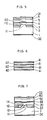
- a striped Si3N4 film is formed on a p-GaAs substrate 10 by a photolithography method. Then, the remaining portion of the substrate 10 which has not been masked by the striped Si3N4 film 20 is mesa-etched by a well known etching technique, as shown in Figure 2 , resulting in a substrate 1 having a striped portion formed into a mesa 11 , on the top of which the striped Si3N4 film 20 remains.
- n-GaAs current blocking layers 2 and 21 are grown by molecular beam epitaxy, as shown in Figure 3 , in such a manner that the thickness t2 of the n-GaAs layer 2 is smaller than the height t1 of the mesa portion 11 .
- the thickness of the said layers can be easily controlled using a molecular beam epitaxy method.
- the n-GaAs layer 21 which is grown on the Si3N4 film 20 concurrently with the n-GaAs layer 2 on the substrate 1 , except the mesa portion 11 , does not crystallize in a single crystal structure but crystallizes in a polycrystal structure.
- the Si3N4 film 20 is removed together with the n-GaAs layer 21 thereon resulting in the n-GaAs layer 2 alone remaining on the substrate 1 as shown in Figure 4 .
- an etchant such as hydrochloric acid
- selective etching can be carried out if a proper etchant is employed. Since t1 is greater than t2 , the mesa portion 11 of the substrate 1 forms in a terrace 110 structure even though the n-GaAs layer 2 remains on the substrate 1 .
- a p-Ga 0.7 Al 0.3 As cladding layer 3 (the thickness thereof being 1 ⁇ m), a non-doped GaAs active layer 4 (the thickness thereof being 0.08 ⁇ m), a n-Ga 0.7 Al 0.3 As cladding layer 5 (the thickness thereof being 1 ⁇ m) and a n-GaAs cap layer 6 (the thickness thereof being 0.5 ⁇ m) are successively formed by a molecular beam epitaxy, followed by the formation of a n-type electrode 31 and a p-type electrode 32 on the surface of the n-GaAs cap layer 6 and the back face of the substrate 1 by an evaporation process, respectively, resulting in a semiconductor laser as shown in Figure 5 .
- each of the growth layers successively formed on the substrate 1 having a terrace 110 shown in Figure 4 consequently conforms to the terraced form of the substrate 1 as seen from Figure 5 .
- the resulting active layer 4 which is constricted at both sides of the region therein corresponding to the terrace 110 of the substrate 1 , forms a striped region 40 , serving as a light waveguide to stabilize the transverse mode of the laser oscillation.
- the light waveguide in the active layer 4 is adjusted in position to the stripe into which an electric current is injected, while the injected electric current is blocked by the n-GaAs current blocking layer 2 and flows through the mesa portion 11 alone of the substrate 1 .
- the semiconductor laser results in a structure which is superior to the stabilization of the transverse mode.
- a quantum-well heterostructure consisting of, for example, a combination of plural non-doped GaAs well layers 41 (the thickness of each layer being 10 ⁇ 5 mm (100 ⁇ ) and plural non-doped Ga 0.8 Al 0.2 As barrier layers 42 (the thickness of each layer being 3X10 ⁇ 6mm (30 ⁇ )) can be used, instead of the non-doped GaAs active layer 4 shown in Figure 5 , thereby obtaining a semiconductor laser exhibiting a quantum-well effect and a stabilized transverse mode.
- an n-GaAs current blocking layer 22 is grown on the substrate 1 in such a manner that a thickness t2 of the n-GaAs layer 22 is greater than a height t1 of the mesa portion 11 of the substrate 1 , in contrast to the afore-mentioned example, resulting in the formation of a groove 111 on the face of the substrate 1 .
- growth layers such as a p-Ga 0.7 Al 0.3 As cladding layer 30, a non-doped GaAs active layer 44 , a non-Ga 0.7 Al 0.3 As cladding layer 50 and a n-GaAs cap layer 60 can be successively formed on the whole face of the substrate 1 in strict conformity with the grooved form of the substrate 1 , producing a light waveguide in the active layer 44 .
- an n-type electrode 33 and a p-type electrode 34 are likewise formed on the n-GaAs cap layer 6 and the back face of the substrate 1 , respectively.
- GaAlAs-semiconductor lasers produced using molecular beam epitaxy were described above they can be also produced using metal-organic chemical vapor deposition or other crystal growth techniques in such a manner that the growth layers conform to a grooved form of the face of the substrate.
- This invention is also applicable to other semiconductor lasers of InGaP, InGaAlP, InAlAs, InGaAs or InGaAsP systems, or the like, in addition to the GaAlAs system.
Landscapes
- Physics & Mathematics (AREA)
- Optics & Photonics (AREA)
- Engineering & Computer Science (AREA)
- Electromagnetism (AREA)
- General Physics & Mathematics (AREA)
- Chemical & Material Sciences (AREA)
- Condensed Matter Physics & Semiconductors (AREA)
- Nanotechnology (AREA)
- Geometry (AREA)
- Life Sciences & Earth Sciences (AREA)
- Biophysics (AREA)
- Crystallography & Structural Chemistry (AREA)
- Semiconductor Lasers (AREA)
Claims (3)
- Verfahren zur Herstellung eines Heterostruktur-Halbleiterlasers, welches Verfahren die Bildung eines Substrats (1) mit einer Streifenschicht (20) darauf und die Ätzung des Substrats (1) beinhaltet, um einen Streifenbereich in einer Mesa (11) zu bilden, wobei sich die Streifenschicht (20) auf der Oberseite der Mesa (11) befindet,
dadurch gekennzeichnet, daß das Verfahren aufweist:
Ablagern von Material (21, 2) zur Bildung einer Stromsperrschicht auf der auf der Oberseite der Mesa (11) befindlichen Streifenschicht (20) und auf der übrigen Oberfläche des Substrats um die Mesa, so daß das auf der übrigen Oberfläche des Substrats abgelagerte Material (2) einkristalline Form und eine Dicke, die größer als die Höhe der Mesa, aufweist,
Entfernen des abgelagerten Materials (21) von der Streifenschicht (20) zusammen mit der Streifenschicht (20) durch Ätzung, wodurch die Stromsperrschicht (2) auf der übrigen Fläche des Substrats erhalten wird und der Streifenbereich eine Einsenkung (111) bildet,
aufeinanderfolgendes Beschichten mit aufgewachsenen Kristallschichten (3, 4, 5, 6) zum Laserbetrieb auf der gesamten Oberfläche des Substrats, durch Ablagerungen, die die aufgewachsenen Schichten (3, 4, 5, 6) in genauer Anpassung, wie sie durch Molekularstrahlepitaxie oder metallorganische Gasphasenabscheidung erreichbar ist, an die Einsenkung (111) bilden. - Verfahren nach Anspruch 1, wobei die aufgewachsenen Halbleiterschichten wahlweise eines von den GaAlAs-, InGaP-, InGaAlP-, InAlAs-, InGaAs- und InGaAsP-Systemen enthält.
- Verfahren nach Anspruch 1 oder 2, wobei die aufgewachsenen Schichten durch Molekularstrahlepitaxie oder metallorganische Gasphasenabscheidung gezüchtet sind.
Applications Claiming Priority (2)
| Application Number | Priority Date | Filing Date | Title |
|---|---|---|---|
| JP160681/83 | 1983-08-30 | ||
| JP58160681A JPS6050983A (ja) | 1983-08-30 | 1983-08-30 | 半導体レ−ザ素子の製造方法 |
Publications (3)
| Publication Number | Publication Date |
|---|---|
| EP0136097A2 EP0136097A2 (de) | 1985-04-03 |
| EP0136097A3 EP0136097A3 (en) | 1987-04-29 |
| EP0136097B1 true EP0136097B1 (de) | 1992-12-16 |
Family
ID=15720162
Family Applications (1)
| Application Number | Title | Priority Date | Filing Date |
|---|---|---|---|
| EP19840305876 Expired EP0136097B1 (de) | 1983-08-30 | 1984-08-29 | Verfahren zur Herstellung von Halbleiterlasern |
Country Status (4)
| Country | Link |
|---|---|
| US (1) | US4569721A (de) |
| EP (1) | EP0136097B1 (de) |
| JP (1) | JPS6050983A (de) |
| DE (1) | DE3486006T2 (de) |
Families Citing this family (21)
| Publication number | Priority date | Publication date | Assignee | Title |
|---|---|---|---|---|
| NL8301331A (nl) * | 1983-04-15 | 1984-11-01 | Philips Nv | Halfgeleiderinrichting voor het opwekken of versterken van electromagnetische straling en werkwijze ter vervaardiging daarvan. |
| EP0157555B1 (de) * | 1984-03-27 | 1990-10-03 | Matsushita Electric Industrial Co., Ltd. | Halbleiterlaser und Verfahren zu dessen Fabrikation |
| US4783425A (en) * | 1985-11-06 | 1988-11-08 | Hitachi, Ltd. | Fabrication process of semiconductor lasers |
| JPS62118055A (ja) * | 1985-11-16 | 1987-05-29 | Mitsubishi Heavy Ind Ltd | 可変噴口燃料噴射弁 |
| US4804639A (en) * | 1986-04-18 | 1989-02-14 | Bell Communications Research, Inc. | Method of making a DH laser with strained layers by MBE |
| US4788159A (en) * | 1986-09-18 | 1988-11-29 | Eastman Kodak Company | Process for forming a positive index waveguide |
| JPS63198320A (ja) * | 1987-02-13 | 1988-08-17 | Mitsubishi Electric Corp | 結晶成長方法 |
| JPS63284878A (ja) * | 1987-04-30 | 1988-11-22 | シーメンス、アクチエンゲゼルシヤフト | 埋込み活性層をもつレーザダイオードの製造方法 |
| JPS63299186A (ja) * | 1987-05-29 | 1988-12-06 | Hitachi Ltd | 発光素子 |
| DE3732822A1 (de) * | 1987-09-29 | 1989-04-06 | Siemens Ag | Laserdiode mit indexfuehrung, insbesondere laserdioden-array mit wellenleiterstruktur |
| JP2655415B2 (ja) * | 1988-04-14 | 1997-09-17 | 石川島播磨重工業株式会社 | 燃料噴射装置 |
| US5202285A (en) * | 1990-04-26 | 1993-04-13 | Fujitsu Limited | Semiconductor laser having double heterostructure and method of producing same |
| US5255281A (en) * | 1990-04-26 | 1993-10-19 | Fujitsu Limited | Semiconductor laser having double heterostructure |
| EP0454476A3 (en) * | 1990-04-26 | 1992-04-01 | Fujitsu Limited | Semiconductor laser having double heterostructure and method of producing the same |
| JP2737477B2 (ja) * | 1991-09-27 | 1998-04-08 | 日本電気株式会社 | 半導体レーザの製造方法 |
| JP3242967B2 (ja) * | 1992-01-31 | 2001-12-25 | 株式会社東芝 | 半導体発光素子 |
| JPH065976A (ja) * | 1992-06-24 | 1994-01-14 | Fujitsu Ltd | 半導体レーザ装置の製造方法 |
| US5384151A (en) * | 1993-08-11 | 1995-01-24 | Northwestern University | InGaAsP/GaAs diode laser |
| JP2956869B2 (ja) * | 1993-08-30 | 1999-10-04 | 富士通株式会社 | 半導体レーザおよびその製造方法 |
| JP2822868B2 (ja) * | 1993-12-10 | 1998-11-11 | 日本電気株式会社 | 半導体レーザの製造方法 |
| US12170436B2 (en) | 2022-01-05 | 2024-12-17 | Modulight Oy | Method for fabricating semiconductor device |
Family Cites Families (4)
| Publication number | Priority date | Publication date | Assignee | Title |
|---|---|---|---|---|
| US4149175A (en) * | 1975-06-20 | 1979-04-10 | Matsushita Electric Industrial Co., Ltd. | Solidstate light-emitting device |
| US4425650A (en) * | 1980-04-15 | 1984-01-10 | Nippon Electric Co., Ltd. | Buried heterostructure laser diode |
| US4347611A (en) * | 1980-11-06 | 1982-08-31 | Xerox Corporation | Large optical cavity (LOC) mesa laser |
| DE3105786A1 (de) * | 1981-02-17 | 1982-09-02 | Siemens AG, 1000 Berlin und 8000 München | Herstellung von lumineszenz- oder laserdioden mit intern begrenzter leuchtflaeche |
-
1983
- 1983-08-30 JP JP58160681A patent/JPS6050983A/ja active Pending
-
1984
- 1984-08-27 US US06/644,437 patent/US4569721A/en not_active Expired - Lifetime
- 1984-08-29 EP EP19840305876 patent/EP0136097B1/de not_active Expired
- 1984-08-29 DE DE8484305876T patent/DE3486006T2/de not_active Expired - Fee Related
Also Published As
| Publication number | Publication date |
|---|---|
| DE3486006T2 (de) | 1993-04-15 |
| EP0136097A3 (en) | 1987-04-29 |
| JPS6050983A (ja) | 1985-03-22 |
| US4569721A (en) | 1986-02-11 |
| EP0136097A2 (de) | 1985-04-03 |
| DE3486006D1 (de) | 1993-01-28 |
Similar Documents
| Publication | Publication Date | Title |
|---|---|---|
| EP0136097B1 (de) | Verfahren zur Herstellung von Halbleiterlasern | |
| EP0142845B1 (de) | Verfahren zur Herstellung einer Halbleiterlaservorrichtung | |
| EP0234955B1 (de) | Halbleiterlaser mit streifenförmiger Mesa-Wellenleiterstruktur und dessen Herstellungsverfahren | |
| US4667332A (en) | Semiconductor laser element suitable for production by a MO-CVD method | |
| US5093278A (en) | Method of manufacturing a semiconductor laser | |
| EP0325275B1 (de) | Sichtbares Licht ausstrahlender Halbleiterlaser mit (AlxGa1-x)0.5In0.5P-Kristallschichten und Verfahren zum Züchten eines (AlxGa1-x)0.5In0.5P-Kristalls | |
| JPH07221392A (ja) | 量子細線の作製方法、量子細線、量子細線レーザ、及び量子細線レーザの作製方法、回折格子の作製方法、及び分布帰還型半導体レーザ | |
| EP0209387B1 (de) | Halbleiterlaser-Vorrichtung | |
| US4694460A (en) | Stripe geometry semiconductor laser device | |
| JP3510305B2 (ja) | 半導体レーザの製造方法,及び半導体レーザ | |
| EP0666625B1 (de) | Verfahren zur Herstellung einer Nut in einer Halbleiter-Laserdiode und Halbleiter-Laserdiode | |
| EP0264225B1 (de) | Halbleiterlaservorrichtung und Verfahren zur Herstellung derselben | |
| EP0412582B1 (de) | Halbleiterlaser | |
| US5805628A (en) | Semiconductor laser | |
| JP2564813B2 (ja) | A▲l▼GaInP半導体発光素子 | |
| JPH0632331B2 (ja) | 半導体レ−ザ装置およびその製造方法 | |
| JPH0560275B2 (de) | ||
| JP3410481B2 (ja) | 半導体レーザ素子 | |
| US4358850A (en) | Terraced substrate semiconductor laser | |
| JPH11354880A (ja) | 半導体レーザ素子およびその製造方法 | |
| JP2525617B2 (ja) | 半導体レ−ザの製造方法 | |
| JPH07235725A (ja) | 半導体レーザ素子およびその製造方法 | |
| JP2611486B2 (ja) | 半導体レーザおよびその製造方法 | |
| JPH04171782A (ja) | 化合物半導体レーザ | |
| JPH06275906A (ja) | 半導体レーザ装置及びその製造方法 |
Legal Events
| Date | Code | Title | Description |
|---|---|---|---|
| PUAI | Public reference made under article 153(3) epc to a published international application that has entered the european phase |
Free format text: ORIGINAL CODE: 0009012 |
|
| 17P | Request for examination filed |
Effective date: 19840831 |
|
| AK | Designated contracting states |
Designated state(s): DE GB NL |
|
| PUAL | Search report despatched |
Free format text: ORIGINAL CODE: 0009013 |
|
| AK | Designated contracting states |
Kind code of ref document: A3 Designated state(s): DE GB NL |
|
| 17Q | First examination report despatched |
Effective date: 19900105 |
|
| GRAA | (expected) grant |
Free format text: ORIGINAL CODE: 0009210 |
|
| AK | Designated contracting states |
Kind code of ref document: B1 Designated state(s): DE GB NL |
|
| REF | Corresponds to: |
Ref document number: 3486006 Country of ref document: DE Date of ref document: 19930128 |
|
| RIN2 | Information on inventor provided after grant (corrected) |
Free format text: HAYAKAWA, TOSHIRO * MIYAUCHI, NOBUYUKI * YANO, SEIKI * SUYAMA, TAKAHIRO |
|
| PLBE | No opposition filed within time limit |
Free format text: ORIGINAL CODE: 0009261 |
|
| STAA | Information on the status of an ep patent application or granted ep patent |
Free format text: STATUS: NO OPPOSITION FILED WITHIN TIME LIMIT |
|
| 26N | No opposition filed | ||
| PGFP | Annual fee paid to national office [announced via postgrant information from national office to epo] |
Ref country code: GB Payment date: 19980820 Year of fee payment: 15 |
|
| PGFP | Annual fee paid to national office [announced via postgrant information from national office to epo] |
Ref country code: NL Payment date: 19980827 Year of fee payment: 15 |
|
| PGFP | Annual fee paid to national office [announced via postgrant information from national office to epo] |
Ref country code: DE Payment date: 19980907 Year of fee payment: 15 |
|
| PG25 | Lapsed in a contracting state [announced via postgrant information from national office to epo] |
Ref country code: GB Free format text: LAPSE BECAUSE OF NON-PAYMENT OF DUE FEES Effective date: 19990829 |
|
| PG25 | Lapsed in a contracting state [announced via postgrant information from national office to epo] |
Ref country code: NL Free format text: LAPSE BECAUSE OF NON-PAYMENT OF DUE FEES Effective date: 20000301 |
|
| GBPC | Gb: european patent ceased through non-payment of renewal fee |
Effective date: 19990829 |
|
| NLV4 | Nl: lapsed or anulled due to non-payment of the annual fee |
Effective date: 20000301 |
|
| PG25 | Lapsed in a contracting state [announced via postgrant information from national office to epo] |
Ref country code: DE Free format text: LAPSE BECAUSE OF NON-PAYMENT OF DUE FEES Effective date: 20000601 |
|
| APAH | Appeal reference modified |
Free format text: ORIGINAL CODE: EPIDOSCREFNO |