EP0122752B1 - Digital-Videobandaufzeichnungsgerät - Google Patents
Digital-Videobandaufzeichnungsgerät Download PDFInfo
- Publication number
- EP0122752B1 EP0122752B1 EP84302300A EP84302300A EP0122752B1 EP 0122752 B1 EP0122752 B1 EP 0122752B1 EP 84302300 A EP84302300 A EP 84302300A EP 84302300 A EP84302300 A EP 84302300A EP 0122752 B1 EP0122752 B1 EP 0122752B1
- Authority
- EP
- European Patent Office
- Prior art keywords
- data
- pulse signal
- supplied
- clock pulse
- phase
- Prior art date
- Legal status (The legal status is an assumption and is not a legal conclusion. Google has not performed a legal analysis and makes no representation as to the accuracy of the status listed.)
- Expired - Lifetime
Links
Images


Classifications
-
- G—PHYSICS
- G11—INFORMATION STORAGE
- G11B—INFORMATION STORAGE BASED ON RELATIVE MOVEMENT BETWEEN RECORD CARRIER AND TRANSDUCER
- G11B20/00—Signal processing not specific to the method of recording or reproducing; Circuits therefor
- G11B20/10—Digital recording or reproducing
- G11B20/14—Digital recording or reproducing using self-clocking codes
- G11B20/1403—Digital recording or reproducing using self-clocking codes characterised by the use of two levels
-
- H—ELECTRICITY
- H04—ELECTRIC COMMUNICATION TECHNIQUE
- H04N—PICTORIAL COMMUNICATION, e.g. TELEVISION
- H04N5/00—Details of television systems
- H04N5/76—Television signal recording
- H04N5/91—Television signal processing therefor
- H04N5/93—Regeneration of the television signal or of selected parts thereof
- H04N5/935—Regeneration of digital synchronisation signals
Definitions
- This invention relates to digital video tape recorder apparatus, and is particularly concerned with the regeneration of a clock pulse signal from a stream of data being reproduced by a digital video tape recorder (VTR) from a magnetic tape.
- VTR digital video tape recorder
- Clock pulse signal recovery is a particular problem where data are being derived from a noisy source, such as off tape by a digital VTR. Because of the high sampling rate required to digitize a television signal, there is generally no spare capacity available when recording on a digital VTR to record clock information, and regeneration from the reproduced stream of data is therefore necessary.
- a PLL circuit arrangement can be designed with some of the characteristics of a tuned circuit, in particular a narrow bandwidth and a strong pickup of the required frequency, but with the additional advantage that in the temporary absence of incoming clock information the PLL circuit can effectively act as a sample-and-hold circuit, with the output continuing at a value determined by the last-received clock information.
- each field of the data contains a substantial amount of useful information, but for some 10% of each rotation of the magnetic head assembly of the VTR no useful data is derived because the magnetic head is not engaging the tape.
- the envelope of the derived data which envelope has a frequency of 50 Hz, therefore includes some 90% with useful clock information, although even in this part of the envelope there may be significant gaps in the clock information due to drop-out on reproduction or to the characteristics of the actual picture content represented by the data.
- the PLL circuit has the ability to bridge any such gap and to pickup and correct quickly to any change in the clock frequency following such a gap.
- FIG. 1 of the accompanying drawings shows a previously-proposed PLL circuit arrangement for clock regeneration.
- Data derived from the tape of a single-speed digital VTR is supplied by way of an input terminal 1 to one input of an exclusive-OR gate 2, the incoming data from the input terminal 1 also being supplied by way of a delay device 3 which introduces a delay of t, to a second input of the exclusive-OR gate 2.
- the output of the exclusive-OR gate 2 is connected to respective inputs of AND gates 4 and 5, the outputs of which, inverted in the case of the AND gate 5, are connected to respective current pump circuits 6 and 7, the outputs of which are connected in common to a loop filter 8.
- the output of the loop filter 8 is a voltage which is supplied to a voltage controlled oscillator (VCO) 9 which produces a clock signal CLK and also an inverted clock signal CLK, the clock frequency being controlled in dependence on the voltage supplied by the loop filter 8.
- VCO voltage controlled oscillator
- the clock signal CLK and the inverted clock signal CLK are respectively supplied to second input terminals of the ANO gates 4 and 5.
- the operation is as follows.
- the exclusive-OR gate 2 and the delay device 3 together have the effect of differentiating the incoming data, and at the output of the exclusive-OR gate 2 there are produced pulses of duration t, one such pulse being produced for each edge, both positive and negative, of the incoming data. It is necessary that t be less than, or at most equal to, half the clock period of the incoming data.
- phase detector this particular form of phase detector is sometimes called a charge pump phase detector.
- the loop filter 8 largely determines the characteristics of the phase-locked loop.
- the operating frequency is 50 MHz
- the hold range is ⁇ 500 KHz
- the capture range is 1 MHz
- the loop bandwidth is 200 KHz
- the accuracy of data regeneration is within ⁇ 1 nanosecond.
- US patent specification US-A-3 900 890 discloses a digital data tape handling system having features generally similarto the pre-characterising part of claim 1.
- digital video tape recorder apparatus comprising:
- embodiments of the present invention provides a dual PLL circuit arrangement which combines the characteristic of having a very wide lock range and a very narrow filter bandwidth, and voltage controlled oscillators in each PLL are preset in dependence on the tape transport speed and direction.
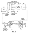
- FIG. 2 this shows part of a magnetic tape 10 from which data are to be reproduced by a variable-speed digital VTR 20 forming part of the embodiment of Figure 3.
- Data are recorded in skew tracks 11, and constant frequency pulses are recorded in a longitudinal track 12 on the tape 10.
- the VTR 20 comprises a capstan 13 for transporting the tape 10 at controllable different speeds about a drum assembly (not shown).
- a direction sensor 14 for sensing the direction of rotation of the capstan 13 and hence the direction of transport of the tape 10.
- the drum assembly includes at least one rotary reproducing head 15 for reproducing the data from the skew tracks 11, and associated with the drum assembly is a fixed reproducing head 16 for reproducing the pulses from the longitudinal track 12.
- the VTR 20 has various reproducing modes including in particular a so-called shuttle mode in which the speed of transport of the tape 10 can be varied over a range from a high speed in the reverse direction through zero to a high speed in the normal forward direction.
- a high speed may be meant up to thirty to fifty times the normal reproducing speed.
- the direction sensor 14 supplies a tape direction signal indicating the direction of transport of the tape 10
- the rotary head 15 supplies the reproduced data
- the fixed head supplies the off tape pulses at a frequency proportional to the tape speed.
- the embodiment to be described comprises the VTR 20, a first PLL circuit arrangement 21 generally as described above with reference to Figure 1, a second PLL circuit arrangement 22, and a preset control signal generator arrangement 23.
- the incoming data is supplied directly and by way of the delay device 3 to respective inputs of the exclusive-OR gate 2.
- the output of the exclusive-OR gate 2 is connected to the remainder of the first PLL circuit arrangement 21 comprising the charge pump phase detector, the loop filter and the VCO which are generally as shown in Figure 1 but are not shown separately in Figure 2.
- the first PLL circuit arrangement 21 produces a regenerated clock pulse signal which is supplied to the input of the second PLL circuit arrangement 22. This regenerated clock pulse signal has too much jitter to be used directly for data regeneration.
- the second PLL circuit arrangement 22 comprises a phase frequency detector in the form of a digital storage phase detector which can operate with a very narrow frequency bandwidth and does not suffer from lock out, that is, the capture range always equals the lock range. It cannot lock out because it is a phase and frequency detector and not merely a phase detector. Thus, if, for example, the frequency is too low, this is positively indicated. However, the PLL circuit arrangement 22 cannot be used alone, because there is insufficient clock information in the incoming data supplied to the input terminal 1.
- the first PLL circuit arrangement 21 has been modified to increase each of the capture range, the hold range and the loop bandwidth by a factor of six.
- the effect of this is that the regenerated clock pulse signal supplied by the first PLL circuit arrangement 21 to the second PLL circuit arrangement 22 is insufficiently filtered for direct use, but this regenerated clock pulse signal has the noisy component filtered out to the required bandwidth of 100 KHz by the second PLL circuit arrangement 22, which supplies an output filtered clock pulse signal to an output terminal 24.
- the second PLL circuit arrangement 22 comprises the phase frequency detector, a loop filter and a VCO, the latter two elements being generally similar to those shown in Figure 1.
- the phase frequency detector may be generally as described in "Phase Lock Techniques” by F M Gardner, 2nd Edition, Wiley, page 123 or "Motorola MECL Handbook” 1978, Pages 6-72 to 6-76.
- a VCO preset control signal is supplied to the respective VCOs in the first and second PLL circuit arrangements 21 and 22 to effect coarse control of their operating frequencies. Provision of such a VCO preset control signal substantially eases the circuit design.
- the preset control signal generator arrangement 23 comprises a counter 25, a reset signal generator 26, a programmable read-only memory (PROM) 27 and a digital-to-analog (D/A) converter 28.
- the VTR 20 supplies the off tape pulses derived by the fixed head 16 ( Figure 2) to the clock input of the counter 25 which is reset to zero at the end of successive regular intervals of time by a reset signal applied to the clear terminal of the counter 25.
- the count immediately prior to each reset operation is a speed signal which is supplied in the form of an 8- bit input to the PROM 27, which also receives the tape direction signal from the direction sensor 14 ( Figure 2) which indicates whether the preset control signal must go up or down.
- the PROM 27, which is in effect operating as a linearity controller, derives an 8-bit digital preset control signal which is converted by the D/A converter 28 to the preset control signal for supply to the VCOs in the first and second PLL circuit arrangements 21 and 22.
- the effect is that although the first and second PLL circuit arrangements as a whole have a loop bandwidth of only a few percent of the incoming frequency so as to achieve reasonable filtering, and hence there is only a narrow capture range, this capture range can be moved up and down in dependence on the incoming data rate.
- the intervals at which the counter 25 is reset depend primarily on the response time of the tape transport mechanism.
- the interval may be say 0.1 second, but if the mechanism is more sluggish then the interval may be say one second.
- the reset signal generator 26 may be any suitable reference timer or interval oscillator in the system.
- the first and second PLL circuit arrangements 21 and 22 will now be further described with reference to Figure 4.
- the data from the exclusive OR gate 2 ( Figure 3) is supplied by way of an input terminal 32 to the first PLL circuit 21 which comprises a phase detector 33, a loop filter 34 having a relatively wide bandwidth and a VCO 35.
- the output supplied by the VCO 35 is a first regenerated clock pulse signal which is supplied to the phase detector 33 and also to a phase frequency detector 36 of the second PLL circuit 22.
- the second PLL circuit 22 also includes a loop filter 38 having a relatively narrow bandwidth and a VCO 39 similar to the VCO 35.
- the output of the VCO 39 is the required output regenerated clock pulse signal and is supplied to the phase frequency detector 36, to the output terminal 24 and also to a latch circuit 40.
- the stream of data supplied to the input terminal 32 is also supplied to a timing circuit 41 to effect any required delay and is then supplied to the latch circuit 40 which is latched under control of the regenerated clock pulse signal, so as to supply the required regenerated output data to an output terminal 42.
- An input terminal 43 is connected to the VCOs 35 and 39 for the supply thereto of the preset control signal.
- the operation is as follows.
- the incoming stream of data from the VTR 20 which is supplied to the input terminal 32 is deficient in clock information, and moreover may vary in data rate over a fairly substantial range, in particular when the reproducing mode of the VTR 20 is changed to achieve a special effect.
- the bandwidth of the loop filter 34 is however such as to ensure that the first PLL circuit 21 has a wide capture range.
- the VCO 35 supplies the continuous first regenerated clock pulse signal to the second PLL circuit 22.
- the bandwidth of the loop filter 38 is such that the PLL circuit 22 has a relatively narrow capture range and the VCO 39 supplies the required output regenerated clock pulse signal.
- VCOs 35 and 39 in the first and second PLL circuit arrangements are similar so that they can be controlled by the same preset control signal, this is not essential. If their control characteristics are different, then appropriate respective preset control signals can be derived for each of them by the PROM 27.
Landscapes
- Engineering & Computer Science (AREA)
- Signal Processing (AREA)
- Multimedia (AREA)
- Signal Processing For Digital Recording And Reproducing (AREA)
- Stabilization Of Oscillater, Synchronisation, Frequency Synthesizers (AREA)
- Television Signal Processing For Recording (AREA)
- Optical Record Carriers And Manufacture Thereof (AREA)
- Fax Reproducing Arrangements (AREA)
Claims (4)
gekennzeichnet durch
Priority Applications (1)
| Application Number | Priority Date | Filing Date | Title |
|---|---|---|---|
| AT84302300T ATE60180T1 (de) | 1983-04-12 | 1984-04-04 | Digital-videobandaufzeichnungsgeraet. |
Applications Claiming Priority (2)
| Application Number | Priority Date | Filing Date | Title |
|---|---|---|---|
| GB8309815 | 1983-04-12 | ||
| GB08309815A GB2138227B (en) | 1983-04-12 | 1983-04-12 | Digital video tape recorder apparatus |
Publications (3)
| Publication Number | Publication Date |
|---|---|
| EP0122752A2 EP0122752A2 (de) | 1984-10-24 |
| EP0122752A3 EP0122752A3 (en) | 1986-11-20 |
| EP0122752B1 true EP0122752B1 (de) | 1991-01-16 |
Family
ID=10540934
Family Applications (1)
| Application Number | Title | Priority Date | Filing Date |
|---|---|---|---|
| EP84302300A Expired - Lifetime EP0122752B1 (de) | 1983-04-12 | 1984-04-04 | Digital-Videobandaufzeichnungsgerät |
Country Status (6)
| Country | Link |
|---|---|
| US (1) | US4577241A (de) |
| EP (1) | EP0122752B1 (de) |
| JP (1) | JPS59198516A (de) |
| AT (1) | ATE60180T1 (de) |
| DE (1) | DE3483915D1 (de) |
| GB (1) | GB2138227B (de) |
Families Citing this family (18)
| Publication number | Priority date | Publication date | Assignee | Title |
|---|---|---|---|---|
| GB8432552D0 (en) * | 1984-12-21 | 1985-02-06 | Plessey Co Plc | Control circuits |
| JPH0772982B2 (ja) * | 1985-09-20 | 1995-08-02 | 株式会社日立製作所 | 情報記録再生装置 |
| US4804925A (en) * | 1986-03-26 | 1989-02-14 | Fuji Photo Film Co., Ltd. | DPSK exclusive-OR demodulator |
| JPH0748723B2 (ja) * | 1987-04-17 | 1995-05-24 | 三洋電機株式会社 | デ−タクロツク発生回路 |
| US5758010A (en) * | 1987-03-19 | 1998-05-26 | Canon Kabushiki Kaisha | Reproducing apparatus with time base corrector |
| JPH0770166B2 (ja) * | 1987-03-20 | 1995-07-31 | 株式会社日立製作所 | ビツト同期回路 |
| JP2661062B2 (ja) * | 1987-09-21 | 1997-10-08 | ソニー株式会社 | データ再生装置 |
| US5045956A (en) * | 1987-12-01 | 1991-09-03 | Matsushita Electric Industrial Co., Ltd. | Data reproducing apparatus |
| US4851932A (en) * | 1988-01-29 | 1989-07-25 | Storage Technology Corporation | Adaptive compensation circuit for moving data storage media |
| JPH027203A (ja) * | 1988-06-27 | 1990-01-11 | Hitachi Ltd | 再生等化回路 |
| US4875108A (en) * | 1988-08-02 | 1989-10-17 | Magnetic Peripherals Inc. | Phase lock loop |
| US5164966A (en) * | 1991-03-07 | 1992-11-17 | The Grass Valley Group, Inc. | Nrz clock and data recovery system employing phase lock loop |
| GB2268614B (en) * | 1992-07-06 | 1996-01-10 | Sony Broadcast & Communication | Digital signal recording |
| KR970003810B1 (ko) * | 1993-04-14 | 1997-03-22 | 삼성전자 주식회사 | 어드레스 천이 검출회로를 내장하는 불휘발성 반도체 집적회로 |
| US6215835B1 (en) * | 1997-08-22 | 2001-04-10 | Lsi Logic Corporation | Dual-loop clock and data recovery for serial data communication |
| US6842056B1 (en) * | 2003-06-24 | 2005-01-11 | Intel Corporation | Cascaded phase-locked loops |
| US7903679B1 (en) * | 2006-04-11 | 2011-03-08 | Altera Corporation | Power supply filtering for programmable logic device having heterogeneous serial interface architecture |
| ES2551583T3 (es) * | 2010-11-23 | 2015-11-20 | Abb Technology Ag | Método y circuito para recuperación de reloj de un flujo de datos |
Family Cites Families (7)
| Publication number | Priority date | Publication date | Assignee | Title |
|---|---|---|---|---|
| US3731220A (en) * | 1972-05-30 | 1973-05-01 | Honeywell Inf Systems | Phase locked oscillator for use with variable speed data source |
| US3898580A (en) * | 1973-12-17 | 1975-08-05 | Xerox Corp | Dual time constant phase lock oscillator |
| US3900890A (en) * | 1974-05-06 | 1975-08-19 | Sperry Rand Corp | Speed tolerant recording and recovery system |
| GB1531632A (en) * | 1976-05-28 | 1978-11-08 | Westinghouse Brake & Signal | Phase-locked loop arrangements |
| DE2823343B1 (de) * | 1978-05-29 | 1979-08-16 | Siemens Ag | Verfahren und Anordnung zur Taktsignalrueckgewinnung bei digitaler Signaluebertragung |
| US4231071A (en) * | 1978-07-17 | 1980-10-28 | Digital Equipment Corporation | Reader for data recorded on magnetic disks at plural densities |
| GB2084415A (en) * | 1980-09-12 | 1982-04-07 | Sony Corp | Apparatus for regenerating a clock pulse signal from a stream of data |
-
1983
- 1983-04-12 GB GB08309815A patent/GB2138227B/en not_active Expired
-
1984
- 1984-03-21 US US06/591,871 patent/US4577241A/en not_active Expired - Lifetime
- 1984-04-04 EP EP84302300A patent/EP0122752B1/de not_active Expired - Lifetime
- 1984-04-04 AT AT84302300T patent/ATE60180T1/de not_active IP Right Cessation
- 1984-04-04 DE DE8484302300T patent/DE3483915D1/de not_active Expired - Lifetime
- 1984-04-12 JP JP59073775A patent/JPS59198516A/ja active Pending
Also Published As
| Publication number | Publication date |
|---|---|
| GB8309815D0 (en) | 1983-05-18 |
| GB2138227B (en) | 1987-02-04 |
| US4577241A (en) | 1986-03-18 |
| ATE60180T1 (de) | 1991-02-15 |
| JPS59198516A (ja) | 1984-11-10 |
| EP0122752A2 (de) | 1984-10-24 |
| EP0122752A3 (en) | 1986-11-20 |
| GB2138227A (en) | 1984-10-17 |
| DE3483915D1 (de) | 1991-02-21 |
Similar Documents
| Publication | Publication Date | Title |
|---|---|---|
| EP0122752B1 (de) | Digital-Videobandaufzeichnungsgerät | |
| EP0258042B1 (de) | Phasenregelschleifenschaltung mit schnell wiederherstellbarer Stabilität | |
| US4195317A (en) | Video recording and playback editing system with displayed cue signals | |
| US4930027A (en) | Method and apparatus for tape speed override operation when recovering helical audio | |
| US4216504A (en) | Slow motion color video recording and playback system | |
| EP0395347B1 (de) | System zur Wiedergewinnung der Abtastfrequenz | |
| GB2084415A (en) | Apparatus for regenerating a clock pulse signal from a stream of data | |
| US5005079A (en) | Automatic frequency control circuit | |
| EP0489375B1 (de) | Trommelservosystem | |
| US5758010A (en) | Reproducing apparatus with time base corrector | |
| US4876614A (en) | Track-readjusted magnetic-tape recorder with transverse tracking | |
| US4862299A (en) | Clock signal regenerator | |
| KR100423177B1 (ko) | 디지탈신호기록/재생장치및방법 | |
| JPH0434768A (ja) | クロツク抽出回路 | |
| JP3028819B2 (ja) | Pll回路のロツク,アンロツク検出回路 | |
| JPH01155571A (ja) | クロック発生回路 | |
| JPS60134683A (ja) | 磁気記録再生装置 | |
| JPS6214900B2 (de) | ||
| JP3031088B2 (ja) | 磁気記録再生装置 | |
| JPS61162854A (ja) | つなぎ撮り制御回路 | |
| JPH0547905B2 (de) | ||
| KR940009973B1 (ko) | 영상신호기록 재생장치 | |
| JP2782435B2 (ja) | 回転ヘツド型ビデオ信号再生装置 | |
| JPS587988A (ja) | 磁気記録再生装置 | |
| JPH06309810A (ja) | クロック再生回路 |
Legal Events
| Date | Code | Title | Description |
|---|---|---|---|
| PUAI | Public reference made under article 153(3) epc to a published international application that has entered the european phase |
Free format text: ORIGINAL CODE: 0009012 |
|
| AK | Designated contracting states |
Designated state(s): AT DE FR GB NL |
|
| PUAL | Search report despatched |
Free format text: ORIGINAL CODE: 0009013 |
|
| AK | Designated contracting states |
Kind code of ref document: A3 Designated state(s): AT DE FR GB NL |
|
| 17P | Request for examination filed |
Effective date: 19870409 |
|
| 17Q | First examination report despatched |
Effective date: 19890724 |
|
| GRAA | (expected) grant |
Free format text: ORIGINAL CODE: 0009210 |
|
| AK | Designated contracting states |
Kind code of ref document: B1 Designated state(s): AT DE FR GB NL |
|
| REF | Corresponds to: |
Ref document number: 60180 Country of ref document: AT Date of ref document: 19910215 Kind code of ref document: T |
|
| ET | Fr: translation filed | ||
| REF | Corresponds to: |
Ref document number: 3483915 Country of ref document: DE Date of ref document: 19910221 |
|
| PLBE | No opposition filed within time limit |
Free format text: ORIGINAL CODE: 0009261 |
|
| STAA | Information on the status of an ep patent application or granted ep patent |
Free format text: STATUS: NO OPPOSITION FILED WITHIN TIME LIMIT |
|
| 26N | No opposition filed | ||
| REG | Reference to a national code |
Ref country code: GB Ref legal event code: IF02 |
|
| PGFP | Annual fee paid to national office [announced via postgrant information from national office to epo] |
Ref country code: GB Payment date: 20030403 Year of fee payment: 20 |
|
| PGFP | Annual fee paid to national office [announced via postgrant information from national office to epo] |
Ref country code: FR Payment date: 20030417 Year of fee payment: 20 |
|
| PGFP | Annual fee paid to national office [announced via postgrant information from national office to epo] |
Ref country code: AT Payment date: 20030423 Year of fee payment: 20 |
|
| PGFP | Annual fee paid to national office [announced via postgrant information from national office to epo] |
Ref country code: NL Payment date: 20030430 Year of fee payment: 20 |
|
| PGFP | Annual fee paid to national office [announced via postgrant information from national office to epo] |
Ref country code: DE Payment date: 20030627 Year of fee payment: 20 |
|
| PG25 | Lapsed in a contracting state [announced via postgrant information from national office to epo] |
Ref country code: GB Free format text: LAPSE BECAUSE OF EXPIRATION OF PROTECTION Effective date: 20040403 |
|
| PG25 | Lapsed in a contracting state [announced via postgrant information from national office to epo] |
Ref country code: NL Free format text: LAPSE BECAUSE OF EXPIRATION OF PROTECTION Effective date: 20040404 Ref country code: AT Free format text: LAPSE BECAUSE OF EXPIRATION OF PROTECTION Effective date: 20040404 |
|
| REG | Reference to a national code |
Ref country code: GB Ref legal event code: PE20 |
|
| NLV7 | Nl: ceased due to reaching the maximum lifetime of a patent |
Effective date: 20040404 |