EP0120834A1 - Filtres optiques texturés et procédé de fabrication - Google Patents
Filtres optiques texturés et procédé de fabrication Download PDFInfo
- Publication number
- EP0120834A1 EP0120834A1 EP84890035A EP84890035A EP0120834A1 EP 0120834 A1 EP0120834 A1 EP 0120834A1 EP 84890035 A EP84890035 A EP 84890035A EP 84890035 A EP84890035 A EP 84890035A EP 0120834 A1 EP0120834 A1 EP 0120834A1
- Authority
- EP
- European Patent Office
- Prior art keywords
- filter layer
- ions
- pattern
- different
- filter
- Prior art date
- Legal status (The legal status is an assumption and is not a legal conclusion. Google has not performed a legal analysis and makes no representation as to the accuracy of the status listed.)
- Granted
Links
Images

Classifications
-
- G—PHYSICS
- G03—PHOTOGRAPHY; CINEMATOGRAPHY; ANALOGOUS TECHNIQUES USING WAVES OTHER THAN OPTICAL WAVES; ELECTROGRAPHY; HOLOGRAPHY
- G03F—PHOTOMECHANICAL PRODUCTION OF TEXTURED OR PATTERNED SURFACES, e.g. FOR PRINTING, FOR PROCESSING OF SEMICONDUCTOR DEVICES; MATERIALS THEREFOR; ORIGINALS THEREFOR; APPARATUS SPECIALLY ADAPTED THEREFOR
- G03F1/00—Originals for photomechanical production of textured or patterned surfaces, e.g., masks, photo-masks, reticles; Mask blanks or pellicles therefor; Containers specially adapted therefor; Preparation thereof
- G03F1/50—Mask blanks not covered by G03F1/20 - G03F1/34; Preparation thereof
Definitions
- the invention relates to an optically structured filter with largely smooth surfaces, in particular to a work mask for the photolithographic production of microelectronic components, with at least one pattern with different transmission for the electromagnetic radiation to be filtered, and a method for its production.
- a radiation-transmissive carrier material primarily made of synthetic quartz glass
- a layer of metal or metal oxide with a thickness of approximately 80-140 nm, which is optically opaque for the desired wavelength range
- a layer of photoresist with a thickness of at least 300 nm applied and the latter is exposed to wave radiation (ultraviolet or X-ray radiation) or a particle beam (electrons, ions) according to a predetermined pattern.
- This exposure process brings about a changed behavior of the exposed areas of the photoresist with respect to a subsequent wet chemical development process, so that, for example in the case of a photoresist called a positive resist, the previously exposed areas are removed by the development process and those below lying optically opaque layer is accessible at these points for a subsequent wet or plasma chemical etching treatment.
- This removes the optically opaque layer locally, so that after a third chemical process step (reactive plasma etching or wet chemical dissolution of the photoresist), in which the remaining, unexposed areas of the photoresist layer are removed, a work mask made of optical material conforming to the original exposure pattern impermeable material on an optically transparent carrier layer.
- a likewise transparent layer of positive photoresist is applied directly to a radiation-permeable carrier material made of quartz, and the latter, as described above, also involves an exposure process Exposed to ultraviolet radiation or electron beams according to a predetermined pattern.
- the exposed areas of the photoresist are continuously removed down to the transparent carrier material and the remaining, unexposed areas of the photoresis layer are converted into an almost completely radiation-blocking state by implantation of silicon ions in the ultraviolet, so that one is also the original one Exposure pattern-conforming work mask made of optically opaque material on an optically transparent carrier layer.
- lithographic processes in which a layer of photoresist is locally changed in its chemical behavior by different exposure processes (ultraviolet or X-rays, electron or ion radiation). All of the processes also have in common the need for one or more wet chemical or plasma chemical process steps.
- the aim of the invention is to propose a method of the type mentioned at the outset which enables simple production of optically structured filters for electromagnetic radiation, in particular work masks, preferably with structure widths of less than 1 ⁇ m, and avoids the disadvantages of the aforementioned methods.
- the object of the invention is to reduce the previously necessary number of process steps, in particular to avoid the previously necessary wet chemical or plasma chemical process steps with their inherent disadvantages, and on the other hand to produce optically structured filters with a largely smooth, unstructured surface in order to prevent the risk of contamination of the filter .
- the filter layer which has a transmission that is locally homogeneous for the electromagnetic radiation to be filtered, for producing the pattern or patterns or regions with different transmission corresponding to the one to be generated Pattern configuration (s) ions, preferably metal ions with an energy above 1keV, can be implanted.
- Pattern configuration (s) ions preferably metal ions with an energy above 1keV
- the ions penetrate into the filter layer based on the kinetic energy they are given, where they then remain stationary.
- the desired permeability characteristic i.e. At those points where ions are implanted in the layer, zones / areas with changed transmission for the electromagnetic radiation to be filtered of a certain wavelength or in a certain wavelength range are created.
- the method according to the invention there is the additional advantage that, due to the short range of scattered ions in solids (a few 10 nm), the ions remain localized in the immediate vicinity of their point of entry during implantation, so that practically no structure broadening in the filter layer receiving the ions occurs by scattering, as is the case, for example, in electron beam lithography by the formation of secondary electrons when a focused electron beam penetrates a photoresist layer. For this reason, it is possible in the method according to the invention to produce structured filters, such as work masks for optical lithography, with a currently reasonable line width down to 200 nm.
- the pattern is written with a focused metal ion beam which is positioned or guided by electromagnetic deflection.
- the beam from a field emission ion source can currently be bundled to a diameter of 40 nm in conventional systems. With such a beam, structures with a line width of approximately 50 nm can be produced in a simple manner.
- Another advantage of the method in question is that by varying the implantation process, areas or patterns with different transmission can be generated for electromagnetic radiation with different wavelengths. This can be done, for example, by varying the ion dose and / or the ion energy. Another possible variation is to implant ions of different elements, molecular ions and ions with different electrical charges.
- Suitable materials for the filter layer are substances that are sufficiently transparent to the radiation to be filtered and that change their transmission through ion implantation.
- Homogeneous or easily homogeneous substances such as organic and inorganic polymers (eg polymethyl methacrylate, silicones), organic and inorganic glasses (eg acrylic glass, synthetic quartz) are particularly suitable.
- organic and inorganic polymers eg polymethyl methacrylate, silicones
- organic and inorganic glasses eg acrylic glass, synthetic quartz
- monocrystalline or polycrystalline substances in particular oxides and nitrides (for example rock crystal, sapphire, silicon nitride) are suitable.
- Metals with a low atomic number are suitable as a filter layer for filters in the low-energy X-ray range.
- the filter layer can be placed on a transparent base layer, e.g. for wavelengths below 400 nm on synthetic quartz.
- a particularly suitable embodiment of the work masks according to the method in question has a filter layer with a max. 400 nm thickness, preferably with 100 to 200 nm thickness.
- These filter layers are on support layers, e.g. made of synthetic quartz glass.
- Such filters are suitable for the UV and far UV range.
- the surface of the filter layer be kept at a constant electrical potential during the implantation process. If the surface of the filter layer is not sufficiently electrically conductive, this can also be achieved by applying a thin electrically conductive layer, preferably a gold layer with a thickness of 3 to 20 nm, to the filter layer before the implantation process. It can be advantageous to remove this conductive layer after the implantation process.
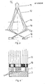
- the filter layer 1 shows a detail of a filter produced according to the method in question.
- the filter layer 1 made of an organic polymer e.g. polymethyl methacrylate
- a carrier 2 made of synthetic quartz glass is built up on a carrier 2 made of synthetic quartz glass.
- Fig. 1 shows the filter both in the top view and in section.
- two patterns 4 are shown which differ in their geometrical arrangement and which have different transmission, but have uniform transmission in the pattern itself.
- the different implantation depths can be seen on average.
- two patterns 4 can be seen, each of which is composed of two areas 5 with different transmissions. Areas of different transmission differ in the type of ion, implantation depth and particle concentration. These differences are achieved by varying the implantation parameters (e.g. ion type, ion energy, ion dose).
- the ion implantation can be carried out in a manner known per se in that an ion beam 12 extracted from an ion source 11 is focused by ion lenses 13 or a combination 13 of such lenses to a diameter which is smaller than the smallest desired structure width of those mask regions 5 which are to be formed with a changed transmission.
- This finely focused ion beam 15 is controlled by a likewise known electrical or magnetic deflection device 14 so that a pattern corresponding to the mask to be produced is implanted with the ion beam 15 in the filter layer 1.
- the ion beam can be fixed in position. remain and the patterns 4 or areas 5 are generated by moving the filter layer 1 under the finely focused ion beam 15 such that the ions are also implanted into the filter layer 1 only in the pattern corresponding to the mask to be produced.
- Is used as ion source 11 e.g. If a liquid metal field emission source is used, a particularly high ion current can be focused in areas of very small dimensions.
- FIG. 3 shows a further known possibility of carrying out the method according to the invention, in which an ion beam 12 delivered by an ion source 11 is used to implant the pattern, or an unbundled or only weakly bundled, penetrating a scaled-up mask 16.
- This mask is projected as an image 18, enlarged or reduced, onto the polymer layer 1 using the imaging device 17.
- a primary mask 16, usually made of metal, is first produced, which is only permeable to the ion beam 12 at the points corresponding to the regions 5 or patterns 4 of the filter.
- This primary mask 16 is illuminated by a long-range ion beam 12, partial ion beams 19 emerging through the recesses of this mask, which are arranged in the form of the mask pattern and hit the filter layer 1 in a focused manner by known ion-optical imaging devices 17.
- the desired reduction or enlargement of the areas or patterns can be achieved by this ion-optical imaging. In this way, the desired patterns can be produced particularly precisely on the work mask, and very thin structure widths can also be achieved.
- FIG. 4 shows another possibility of carrying out the method according to the invention, which consists in bringing a mask 16, which carries the pattern to be written in on a scale of 1: 1, into contact with the filter layer 1 and then being exposed to an unbundled ion beam 12.
- the filter layer 1 can be carried by a substrate 2.
- work masks produced according to the invention are suitable not only for structuring solid surfaces for producing microelectronic components but also for producing components of the integrated optics, for producing one- and two-dimensional diffraction gratings for electromagnetic radiation and for producing zone plates.
- the ion beam 12 was accelerated to an energy of 10 keV and focused in such a way that an ion current of 10 nA simply charged indium, tin or oxygen ions could be bundled into a spot of 5 ⁇ m diameter on the polymer layer 1.
- a pattern was written into the filter layer 1 by electrostatic deflection of the ion beam 15, the local ion dose being approximately 4x10 15 ions / cm 2 .
- the remaining gold layer 3 was chemically detached.
- the usability of this ion-implanted pattern as a work mask for UV exposure was demonstrated by bringing the implanted polymer layer 1 into contact with a positive-working photoresist (Shipley AZ 1350 J, 600 nm thick) spun substrate.
- the exposure was carried out with an ultraviolet light source (high-pressure mercury vapor lamp) with an exposure time of 3.5 s.
- an ultraviolet light source high-pressure mercury vapor lamp
- After developing the thus exposed photoresist spray development 60 s, at 800 rpm with AZ 350 Developer, thinner 5: 1 with deionized water, the structuring of the high edge sharpness specified by the mask resulted in the photoresist layer.
- the masks produced according to the method in question proved to be significantly improved in terms of the service life compared to the usual chromium-chromium oxide work masks, because the high power density of an excimer laser (5 MW / cm 2 ) has been found in surface-coated masks (current state of the art). has a relatively rapid destructive effect on the metal layer.
- the method in question enables the production of very thin masks lying against non-flat surfaces when placed in a very thin self-supporting, transparent film 1, e.g. up to 20 ⁇ m thick.
- Such filters enable the production of structures even on non-flat surfaces according to the principle of contact lithography. It is possible to establish complete contact between the mask and the substrate coated with resist without great effort, which is not possible with the mask materials currently used. With such masks, contact lithography was carried out on cylindrical surfaces with radii of curvature less than 2 mm.
Landscapes
- Physics & Mathematics (AREA)
- General Physics & Mathematics (AREA)
- Preparing Plates And Mask In Photomechanical Process (AREA)
- Shielding Devices Or Components To Electric Or Magnetic Fields (AREA)
- Exposure And Positioning Against Photoresist Photosensitive Materials (AREA)
- Optical Integrated Circuits (AREA)
- Glass Compositions (AREA)
Applications Claiming Priority (2)
| Application Number | Priority Date | Filing Date | Title |
|---|---|---|---|
| AT0071783A AT382040B (de) | 1983-03-01 | 1983-03-01 | Verfahren zur herstellung von optisch strukturierten filtern fuer elektromagnetische strahlung und optisch strukturierter filter |
| AT717/83 | 1983-03-01 |
Publications (2)
| Publication Number | Publication Date |
|---|---|
| EP0120834A1 true EP0120834A1 (fr) | 1984-10-03 |
| EP0120834B1 EP0120834B1 (fr) | 1988-05-25 |
Family
ID=3497959
Family Applications (2)
| Application Number | Title | Priority Date | Filing Date |
|---|---|---|---|
| EP84900947A Withdrawn EP0136317A1 (fr) | 1983-03-01 | 1984-02-27 | Filtre a structure optique et son procede de fabrication |
| EP84890035A Expired EP0120834B1 (fr) | 1983-03-01 | 1984-02-29 | Filtres optiques texturés et procédé de fabrication |
Family Applications Before (1)
| Application Number | Title | Priority Date | Filing Date |
|---|---|---|---|
| EP84900947A Withdrawn EP0136317A1 (fr) | 1983-03-01 | 1984-02-27 | Filtre a structure optique et son procede de fabrication |
Country Status (6)
| Country | Link |
|---|---|
| US (1) | US4686162A (fr) |
| EP (2) | EP0136317A1 (fr) |
| JP (1) | JPS60502120A (fr) |
| AT (2) | AT382040B (fr) |
| DE (1) | DE3471531D1 (fr) |
| WO (1) | WO1984003571A1 (fr) |
Cited By (4)
| Publication number | Priority date | Publication date | Assignee | Title |
|---|---|---|---|---|
| EP0195724A2 (fr) * | 1985-03-20 | 1986-09-24 | Fujitsu Limited | Masque de modulation spatiale de phase, procédé de fabrication et procédé pour la formation de réseaux de diffraction diphasés |
| EP0253066A2 (fr) * | 1986-07-12 | 1988-01-20 | Kernforschungszentrum Karlsruhe Gmbh | Procédé pour réaliser des microstructures à plusieurs niveaux par lithographie aux rayons X |
| EP0265872A2 (fr) * | 1986-10-29 | 1988-05-04 | International Business Machines Corporation | Gravure simultanée de la structure multicouche et de la structure d'image |
| US5395739A (en) * | 1992-12-15 | 1995-03-07 | Mitsubishi Denki Kabushiki Kaisha | Method for producing field effect transistor |
Families Citing this family (48)
| Publication number | Priority date | Publication date | Assignee | Title |
|---|---|---|---|---|
| CA1313792C (fr) * | 1986-02-28 | 1993-02-23 | Junji Hirokane | Methode de fabrication de photomasques et photomasque fabrique selon cette methode |
| JPS6370203A (ja) * | 1986-09-11 | 1988-03-30 | Brother Ind Ltd | 屈折率分布型光導波路レンズの製造方法 |
| JP2706237B2 (ja) * | 1986-09-20 | 1998-01-28 | ブラザー工業株式会社 | レーザプリンタ |
| IT1211939B (it) * | 1987-11-27 | 1989-11-08 | Siv Soc Italiana Vetro | Procedimento per la fabbricazione di vetri con caratteristiche energetiche modificate e prodotto cosi'ottenuto |
| JPH0296159A (ja) * | 1988-10-03 | 1990-04-06 | Sanyo Electric Co Ltd | フォトリソグラフィ用マスクの製造方法 |
| TW198129B (fr) * | 1990-06-21 | 1993-01-11 | Matsushita Electron Co Ltd | |
| US5578402A (en) * | 1990-06-21 | 1996-11-26 | Matsushita Electronics Corporation | Photomask used by photolithography and a process of producing same |
| US5213916A (en) * | 1990-10-30 | 1993-05-25 | International Business Machines Corporation | Method of making a gray level mask |
| US5589305A (en) * | 1990-11-29 | 1996-12-31 | Kabushiki Kaisha Toshiba | Method of fabricating a reticle |
| US5660956A (en) * | 1990-11-29 | 1997-08-26 | Kabushiki Kaisha Toshiba | Reticle and method of fabricating reticle |
| US5217830A (en) * | 1991-03-26 | 1993-06-08 | Micron Technology, Inc. | Method of fabricating phase shifting reticles using ion implantation |
| US5208125A (en) * | 1991-07-30 | 1993-05-04 | Micron Technology, Inc. | Phase shifting reticle fabrication using ion implantation |
| FR2695117B1 (fr) * | 1992-08-28 | 1994-12-02 | Saint Gobain Vitrage Int | Procédé de traitement de couches minces à propriétés de conduction électrique et/ou de réflexion dans l'infra-rouge. |
| US5418095A (en) * | 1993-01-21 | 1995-05-23 | Sematech, Inc. | Method of fabricating phase shifters with absorbing/attenuating sidewalls using an additive process |
| WO1994017449A1 (fr) * | 1993-01-21 | 1994-08-04 | Sematech, Inc. | Structure de masque de decalage de phase comprenant un revetement optique multicouche qui ameliore la transmission |
| US5411824A (en) * | 1993-01-21 | 1995-05-02 | Sematech, Inc. | Phase shifting mask structure with absorbing/attenuating sidewalls for improved imaging |
| US5314768A (en) * | 1993-03-19 | 1994-05-24 | National Semiconductor Corporation | Thin film mask for use in an x-ray lithographic process and its method of manufacture by forming opaque pattern of ions in a diamond layer |
| US5679483A (en) * | 1994-12-20 | 1997-10-21 | Siemens Aktiengesellschaft | Embedded phase shifting photomasks and method for manufacturing same |
| US7658772B2 (en) * | 1997-09-08 | 2010-02-09 | Borealis Technical Limited | Process for making electrode pairs |
| US6106979A (en) | 1997-12-30 | 2000-08-22 | Micron Technology, Inc. | Use of attenuating phase-shifting mask for improved printability of clear-field patterns |
| US6077630A (en) * | 1998-01-08 | 2000-06-20 | Micron Technology, Inc. | Subresolution grating for attenuated phase shifting mask fabrication |
| US6096457A (en) | 1998-02-27 | 2000-08-01 | Micron Technology, Inc. | Method for optimizing printing of a phase shift mask having a phase shift error |
| US5998069A (en) | 1998-02-27 | 1999-12-07 | Micron Technology, Inc. | Electrically programmable photolithography mask |
| US6117344A (en) * | 1998-03-20 | 2000-09-12 | Borealis Technical Limited | Method for manufacturing low work function surfaces |
| US6064511A (en) * | 1998-03-31 | 2000-05-16 | The Research Foundation Of State University Of New York | Fabrication methods and structured materials for photonic devices |
| US6680214B1 (en) * | 1998-06-08 | 2004-01-20 | Borealis Technical Limited | Artificial band gap |
| US20070108437A1 (en) * | 1998-06-08 | 2007-05-17 | Avto Tavkhelidze | Method of fabrication of high temperature superconductors based on new mechanism of electron-electron interaction |
| US7074498B2 (en) * | 2002-03-22 | 2006-07-11 | Borealis Technical Limited | Influence of surface geometry on metal properties |
| US7651875B2 (en) * | 1998-06-08 | 2010-01-26 | Borealis Technical Limited | Catalysts |
| US8574663B2 (en) * | 2002-03-22 | 2013-11-05 | Borealis Technical Limited | Surface pairs |
| DE10241708B4 (de) * | 2002-09-09 | 2005-09-29 | Fraunhofer-Gesellschaft zur Förderung der angewandten Forschung e.V. | Verfahren zur Reduzierung der Grenzflächenreflexion von Kunststoffsubstraten sowie derart modifiziertes Substrat und dessen Verwendung |
| US7244768B2 (en) * | 2003-10-03 | 2007-07-17 | Allergan, Inc. | Compositions and methods comprising prostaglandin related compounds and trefoil factor family peptides for the treatment of glaucoma with reduced hyperemia |
| GB0415426D0 (en) * | 2004-07-09 | 2004-08-11 | Borealis Tech Ltd | Thermionic vacuum diode device with adjustable electrodes |
| US20060028685A1 (en) * | 2004-08-04 | 2006-02-09 | Nicole Proulx | Method for allowing users to specify multiple quality settings on mixed printouts |
| US7550236B2 (en) * | 2004-09-29 | 2009-06-23 | Lsi Corporation | Multi wavelength mask for multi layer printing on a process substrate |
| GB0501413D0 (en) * | 2005-01-24 | 2005-03-02 | Tavkhelidze Avto | Method for modification of built in potential of diodes |
| US20060251971A1 (en) * | 2005-05-03 | 2006-11-09 | Richard Schenker | Photo-Mask with variable transmission by ion implantation |
| GB0515635D0 (en) * | 2005-07-29 | 2005-09-07 | Harbron Stuart | Transistor |
| GB0518132D0 (en) * | 2005-09-06 | 2005-10-12 | Cox Isaiah W | Cooling device using direct deposition of diode heat pump |
| US7427786B1 (en) | 2006-01-24 | 2008-09-23 | Borealis Technical Limited | Diode device utilizing bellows |
| US8227885B2 (en) | 2006-07-05 | 2012-07-24 | Borealis Technical Limited | Selective light absorbing semiconductor surface |
| GB0617934D0 (en) * | 2006-09-12 | 2006-10-18 | Borealis Tech Ltd | Transistor |
| GB0618268D0 (en) * | 2006-09-18 | 2006-10-25 | Tavkhelidze Avto | High efficiency solar cell with selective light absorbing surface |
| GB0700071D0 (en) * | 2007-01-04 | 2007-02-07 | Borealis Tech Ltd | Multijunction solar cell |
| US8816192B1 (en) | 2007-02-09 | 2014-08-26 | Borealis Technical Limited | Thin film solar cell |
| CN102379005B (zh) * | 2009-04-13 | 2016-08-24 | 应用材料公司 | 用离子和中性束注入改变膜的磁性 |
| US20120094220A1 (en) * | 2009-06-20 | 2012-04-19 | Sharp Kabushiki Kaisha | Photo mask, photolithography method, substrate production method and display panel production method |
| KR20170110593A (ko) | 2015-01-05 | 2017-10-11 | 마수피얼 홀딩스 아이엔시. | 멀티톤 레벨 포토마스크 |
Citations (5)
| Publication number | Priority date | Publication date | Assignee | Title |
|---|---|---|---|---|
| DE2623688A1 (de) * | 1975-05-28 | 1976-12-02 | Hitachi Ltd | Verfahren zum ausbilden von mustern bei der herstellung von elektronischen mikrobauteilen |
| US4144066A (en) * | 1977-11-30 | 1979-03-13 | Ppg Industries, Inc. | Electron bombardment method for making stained glass photomasks |
| GB1577479A (en) * | 1976-10-07 | 1980-10-22 | Sony Corp | Optical exposure apparatus |
| GB1583459A (en) * | 1977-12-20 | 1981-01-28 | Philips Electronic Associated | Masks their manufacture and the manufacture of microminiature solid-state devices using such masks |
| GB2079536A (en) * | 1980-07-03 | 1982-01-20 | Commissariat Energie Atomique | Process for producing an optical network |
Family Cites Families (10)
| Publication number | Priority date | Publication date | Assignee | Title |
|---|---|---|---|---|
| US3682729A (en) * | 1969-12-30 | 1972-08-08 | Ibm | Method of changing the physical properties of a metallic film by ion beam formation and devices produced thereby |
| US3940507A (en) * | 1974-05-03 | 1976-02-24 | Rca Corporation | Electron beam recording media and method of recording |
| DE2643811C2 (de) * | 1975-10-28 | 1981-10-15 | Hughes Aircraft Co., Culver City, Calif. | Lithographie-Maske mit einer für Strahlung durchlässigen Membran und Verfahren zu ihrer Herstellung |
| JPS5573047A (en) * | 1978-11-25 | 1980-06-02 | Mitsubishi Electric Corp | Manufacture of photo mask |
| JPS5619623A (en) * | 1979-07-27 | 1981-02-24 | Hitachi Ltd | Photomask |
| JPS5754939A (en) * | 1980-09-19 | 1982-04-01 | Matsushita Electric Ind Co Ltd | Optical mask and its manufacture |
| JPS57102019A (en) * | 1980-12-17 | 1982-06-24 | Mitsubishi Electric Corp | Failure correction of x-ray exposure mask |
| JPS57157248A (en) * | 1981-03-23 | 1982-09-28 | Nec Corp | Preparation of optical exposure mask |
| JPS5893052A (ja) * | 1981-11-30 | 1983-06-02 | Seiko Epson Corp | ホトマスク |
| US4548883A (en) * | 1983-05-31 | 1985-10-22 | At&T Bell Laboratories | Correction of lithographic masks |
-
1983
- 1983-03-01 AT AT0071783A patent/AT382040B/de not_active IP Right Cessation
-
1984
- 1984-02-27 EP EP84900947A patent/EP0136317A1/fr not_active Withdrawn
- 1984-02-27 WO PCT/AT1984/000010 patent/WO1984003571A1/fr unknown
- 1984-02-27 JP JP59501710A patent/JPS60502120A/ja active Pending
- 1984-02-27 US US06/667,493 patent/US4686162A/en not_active Expired - Fee Related
- 1984-02-29 AT AT84890035T patent/ATE34626T1/de not_active IP Right Cessation
- 1984-02-29 DE DE8484890035T patent/DE3471531D1/de not_active Expired
- 1984-02-29 EP EP84890035A patent/EP0120834B1/fr not_active Expired
Patent Citations (5)
| Publication number | Priority date | Publication date | Assignee | Title |
|---|---|---|---|---|
| DE2623688A1 (de) * | 1975-05-28 | 1976-12-02 | Hitachi Ltd | Verfahren zum ausbilden von mustern bei der herstellung von elektronischen mikrobauteilen |
| GB1577479A (en) * | 1976-10-07 | 1980-10-22 | Sony Corp | Optical exposure apparatus |
| US4144066A (en) * | 1977-11-30 | 1979-03-13 | Ppg Industries, Inc. | Electron bombardment method for making stained glass photomasks |
| GB1583459A (en) * | 1977-12-20 | 1981-01-28 | Philips Electronic Associated | Masks their manufacture and the manufacture of microminiature solid-state devices using such masks |
| GB2079536A (en) * | 1980-07-03 | 1982-01-20 | Commissariat Energie Atomique | Process for producing an optical network |
Non-Patent Citations (5)
| Title |
|---|
| CHEMICAL ABSTRACTS, Band 98, Nr. 18, 2. Mai 1983, Seite 543, Nr. 152099a, Columbus, Ohio, USA A.L. KAMARDIN et al.: "Change in optical properties of thin films as a result of ion bombardment" & POVERKHNOST 1982, (4), 87-89 * |
| PATENTS ABSTRACTS OF JAPAN, Band 6, Nr. 104(P-122)(982), 15. Juni 1982 & JP - A - 57 35859 (TOKYO SHIBAURA DENKI K.K.) 26.02.1982 * |
| PATENTS ABSTRACTS OF JAPAN, Band 6, Nr. 129(P-128)(1007), 15. Juli 1982 & JP - A - 57 54939 (MATSUSHITA DENKI SANGYO K.K.) 01.04.1982 * |
| PATENTS ABSTRACTS OF JAPAN, Band 6, Nr. 262(P-164)(1140), 21. Dezember 1982 & JP - A - 57 157 248 (NIPPON DENKI K.K.) 28.09.1982 * |
| PATENTS ABSTRACTS OF JAPAN, Band 7, Nr. 196(P-219)(1341), 26. August 1983 & JP - A - 58 93052 (SUWA SEIKOSHA K.K.) 02.06.1983 * |
Cited By (9)
| Publication number | Priority date | Publication date | Assignee | Title |
|---|---|---|---|---|
| EP0195724A2 (fr) * | 1985-03-20 | 1986-09-24 | Fujitsu Limited | Masque de modulation spatiale de phase, procédé de fabrication et procédé pour la formation de réseaux de diffraction diphasés |
| EP0195724A3 (en) * | 1985-03-20 | 1990-05-16 | Fujitsu Limited | Spatial phase modulating masks and production processes thereof, and processes for the formation of phase-shifted diffraction gratings |
| EP0253066A2 (fr) * | 1986-07-12 | 1988-01-20 | Kernforschungszentrum Karlsruhe Gmbh | Procédé pour réaliser des microstructures à plusieurs niveaux par lithographie aux rayons X |
| EP0253066A3 (fr) * | 1986-07-12 | 1989-11-08 | Kernforschungszentrum Karlsruhe Gmbh | Procédé pour réaliser des microstructures à plusieurs niveaux par lithographie aux rayons X |
| EP0265872A2 (fr) * | 1986-10-29 | 1988-05-04 | International Business Machines Corporation | Gravure simultanée de la structure multicouche et de la structure d'image |
| EP0265872B1 (fr) * | 1986-10-29 | 1995-03-08 | International Business Machines Corporation | Gravure simultanée de la structure multicouche et de la structure d'image |
| US5395739A (en) * | 1992-12-15 | 1995-03-07 | Mitsubishi Denki Kabushiki Kaisha | Method for producing field effect transistor |
| GB2273578B (en) * | 1992-12-15 | 1996-06-12 | Mitsubishi Electric Corp | Method for producing field effect transistor and pattern mask therefor |
| US5547789A (en) * | 1992-12-15 | 1996-08-20 | Mitsubishi Denki Kabushiki Kaisha | Pattern transfer mask |
Also Published As
| Publication number | Publication date |
|---|---|
| JPS60502120A (ja) | 1985-12-05 |
| ATA71783A (de) | 1986-05-15 |
| DE3471531D1 (en) | 1988-06-30 |
| WO1984003571A1 (fr) | 1984-09-13 |
| AT382040B (de) | 1986-12-29 |
| EP0120834B1 (fr) | 1988-05-25 |
| ATE34626T1 (de) | 1988-06-15 |
| EP0136317A1 (fr) | 1985-04-10 |
| US4686162A (en) | 1987-08-11 |
Similar Documents
| Publication | Publication Date | Title |
|---|---|---|
| EP0120834B1 (fr) | Filtres optiques texturés et procédé de fabrication | |
| DE2302116C3 (de) | Vorrichtung zur Herstellung einer maskierenden Schicht auf einem Träger mit Hilfe von weichen Röntgenstrahlen | |
| EP0203215B1 (fr) | Procédé pour la correction des masques par transmission | |
| DE1771076C3 (de) | Verfahren zur Herstellung eines Mosaikschirmes für eine Farbfernsehröhre | |
| DE102006053074B4 (de) | Strukturierungsverfahren unter Verwendung chemisch verstärkter Fotolacke und Belichtungsvorrichtung | |
| DE10059268C1 (de) | Verfahren und Vorrichtung zur Herstellung eines Koppelgitters für einen Wellenleiter | |
| DE3420353C2 (de) | Verfahren zum Korrigieren und Modifizieren von lithographischen Masken | |
| DE2922416A1 (de) | Schattenwurfmaske zum strukturieren von oberflaechenbereichen und verfahren zu ihrer herstellung | |
| DE19628355A1 (de) | Verfahren zur Herstellung von 3-dimensionalen Photonen-Kristallen | |
| EP0739531B1 (fr) | Systeme de reproduction optique par faisceaux de particules | |
| DE2547079A1 (de) | Verfahren zur korpuskularbestrahlung eines praeparats | |
| EP0564438A1 (fr) | Système de formation d'images par faisceau de particules notamment système d'imagerie en optique ionique | |
| DE10309266B3 (de) | Verfahren zum Bilden einer Öffnung einer Licht absorbierenden Schicht auf einer Maske | |
| DE102005044141B4 (de) | Belichtungsgerät und Verfahren zum Betrieb eines Belichtungsgeräts | |
| DE2643811A1 (de) | Verfahren zur herstellung eines musters in einer photolackschicht und hierfuer geeignete maske | |
| EP1456870A2 (fr) | Procede de lithographie sans resistance pour la realisation de structures fines | |
| DE2446789A1 (de) | Korpuskularstrahloptisches geraet zur korpuskelbestrahlung eines praeparats | |
| DE2535156C3 (de) | Verfahren zur Herstellung einer Schicht mit vorgegebenem Muster von Bereichen geringerer Schichtdicke und Verwendung der Schicht als Maske bei der Dotierung | |
| DE2626068A1 (de) | Ionographische aufzeichnung von roentgenbildern | |
| DE4028647C2 (de) | Verfahren zum Kopieren von Lochmasken | |
| DE10253073A1 (de) | Verfahren zur Reparatur einer photolithographischen Maske und eine photolithographische Maske | |
| DE102022213753A1 (de) | Vorrichtung zum Schutz einer Oberfläche vor Schädigung durch auftreffende Ionen | |
| DE102004012240B4 (de) | Verfahren zur Herstellung einer Lochmaske zur lithographischen Strukturierung mittels geladener Teilchen | |
| DE19922758A1 (de) | Verfahren zur Herstellung einer lithographischen Zeichnung | |
| JPH0330313A (ja) | 微細パターン形成方法 |
Legal Events
| Date | Code | Title | Description |
|---|---|---|---|
| PUAI | Public reference made under article 153(3) epc to a published international application that has entered the european phase |
Free format text: ORIGINAL CODE: 0009012 |
|
| AK | Designated contracting states |
Designated state(s): AT BE CH DE FR GB IT LI LU NL SE |
|
| 17P | Request for examination filed |
Effective date: 19850112 |
|
| RAP1 | Party data changed (applicant data changed or rights of an application transferred) |
Owner name: OESTERREICHISCHES FORSCHUNGSZENTRUM SEIBERSDORF GE |
|
| 17Q | First examination report despatched |
Effective date: 19861001 |
|
| GRAA | (expected) grant |
Free format text: ORIGINAL CODE: 0009210 |
|
| RAP3 | Party data changed (applicant data changed or rights of an application transferred) |
Owner name: OESTERREICHISCHES FORSCHUNGSZENTRUM SEIBERSDORF GE |
|
| AK | Designated contracting states |
Kind code of ref document: B1 Designated state(s): AT BE CH DE FR GB IT LI LU NL SE |
|
| PG25 | Lapsed in a contracting state [announced via postgrant information from national office to epo] |
Ref country code: IT Free format text: LAPSE BECAUSE OF FAILURE TO SUBMIT A TRANSLATION OF THE DESCRIPTION OR TO PAY THE FEE WITHIN THE PRESCRIBED TIME-LIMIT;WARNING: LAPSES OF ITALIAN PATENTS WITH EFFECTIVE DATE BEFORE 2007 MAY HAVE OCCURRED AT ANY TIME BEFORE 2007. THE CORRECT EFFECTIVE DATE MAY BE DIFFERENT FROM THE ONE RECORDED. Effective date: 19880525 |
|
| REF | Corresponds to: |
Ref document number: 34626 Country of ref document: AT Date of ref document: 19880615 Kind code of ref document: T |
|
| PG25 | Lapsed in a contracting state [announced via postgrant information from national office to epo] |
Ref country code: SE Effective date: 19880531 |
|
| REF | Corresponds to: |
Ref document number: 3471531 Country of ref document: DE Date of ref document: 19880630 |
|
| GBT | Gb: translation of ep patent filed (gb section 77(6)(a)/1977) | ||
| ET | Fr: translation filed | ||
| PLBE | No opposition filed within time limit |
Free format text: ORIGINAL CODE: 0009261 |
|
| STAA | Information on the status of an ep patent application or granted ep patent |
Free format text: STATUS: NO OPPOSITION FILED WITHIN TIME LIMIT |
|
| 26N | No opposition filed | ||
| PGFP | Annual fee paid to national office [announced via postgrant information from national office to epo] |
Ref country code: GB Payment date: 19930125 Year of fee payment: 10 |
|
| PGFP | Annual fee paid to national office [announced via postgrant information from national office to epo] |
Ref country code: FR Payment date: 19930204 Year of fee payment: 10 |
|
| PGFP | Annual fee paid to national office [announced via postgrant information from national office to epo] |
Ref country code: LU Payment date: 19930209 Year of fee payment: 10 Ref country code: BE Payment date: 19930209 Year of fee payment: 10 |
|
| PGFP | Annual fee paid to national office [announced via postgrant information from national office to epo] |
Ref country code: AT Payment date: 19930218 Year of fee payment: 10 |
|
| PGFP | Annual fee paid to national office [announced via postgrant information from national office to epo] |
Ref country code: NL Payment date: 19930228 Year of fee payment: 10 |
|
| PGFP | Annual fee paid to national office [announced via postgrant information from national office to epo] |
Ref country code: DE Payment date: 19930331 Year of fee payment: 10 |
|
| PGFP | Annual fee paid to national office [announced via postgrant information from national office to epo] |
Ref country code: CH Payment date: 19930407 Year of fee payment: 10 |
|
| EPTA | Lu: last paid annual fee | ||
| PG25 | Lapsed in a contracting state [announced via postgrant information from national office to epo] |
Ref country code: LU Free format text: LAPSE BECAUSE OF NON-PAYMENT OF DUE FEES Effective date: 19940228 Ref country code: LI Effective date: 19940228 Ref country code: GB Effective date: 19940228 Ref country code: CH Effective date: 19940228 Ref country code: BE Effective date: 19940228 Ref country code: AT Effective date: 19940228 |
|
| BERE | Be: lapsed |
Owner name: OSTERREICHISCHES FORSCHUNGSZENTRUM SEIBERSDORF G. Effective date: 19940228 |
|
| PG25 | Lapsed in a contracting state [announced via postgrant information from national office to epo] |
Ref country code: NL Effective date: 19940901 |
|
| NLV4 | Nl: lapsed or anulled due to non-payment of the annual fee | ||
| GBPC | Gb: european patent ceased through non-payment of renewal fee |
Effective date: 19940228 |
|
| PG25 | Lapsed in a contracting state [announced via postgrant information from national office to epo] |
Ref country code: FR Effective date: 19941031 |
|
| REG | Reference to a national code |
Ref country code: CH Ref legal event code: PL |
|
| PG25 | Lapsed in a contracting state [announced via postgrant information from national office to epo] |
Ref country code: DE Effective date: 19941101 |
|
| REG | Reference to a national code |
Ref country code: FR Ref legal event code: ST |