EP0265872B1 - Gravure simultanée de la structure multicouche et de la structure d'image - Google Patents
Gravure simultanée de la structure multicouche et de la structure d'image Download PDFInfo
- Publication number
- EP0265872B1 EP0265872B1 EP87115596A EP87115596A EP0265872B1 EP 0265872 B1 EP0265872 B1 EP 0265872B1 EP 87115596 A EP87115596 A EP 87115596A EP 87115596 A EP87115596 A EP 87115596A EP 0265872 B1 EP0265872 B1 EP 0265872B1
- Authority
- EP
- European Patent Office
- Prior art keywords
- mask
- etching
- layer
- etched
- substrate
- Prior art date
- Legal status (The legal status is an assumption and is not a legal conclusion. Google has not performed a legal analysis and makes no representation as to the accuracy of the status listed.)
- Expired - Lifetime
Links
Images

Classifications
-
- H—ELECTRICITY
- H01—ELECTRIC ELEMENTS
- H01L—SEMICONDUCTOR DEVICES NOT COVERED BY CLASS H10
- H01L24/00—Arrangements for connecting or disconnecting semiconductor or solid-state bodies; Methods or apparatus related thereto
- H01L24/80—Methods for connecting semiconductor or other solid state bodies using means for bonding being attached to, or being formed on, the surface to be connected
-
- B—PERFORMING OPERATIONS; TRANSPORTING
- B23—MACHINE TOOLS; METAL-WORKING NOT OTHERWISE PROVIDED FOR
- B23K—SOLDERING OR UNSOLDERING; WELDING; CLADDING OR PLATING BY SOLDERING OR WELDING; CUTTING BY APPLYING HEAT LOCALLY, e.g. FLAME CUTTING; WORKING BY LASER BEAM
- B23K26/00—Working by laser beam, e.g. welding, cutting or boring
- B23K26/02—Positioning or observing the workpiece, e.g. with respect to the point of impact; Aligning, aiming or focusing the laser beam
- B23K26/06—Shaping the laser beam, e.g. by masks or multi-focusing
- B23K26/064—Shaping the laser beam, e.g. by masks or multi-focusing by means of optical elements, e.g. lenses, mirrors or prisms
- B23K26/066—Shaping the laser beam, e.g. by masks or multi-focusing by means of optical elements, e.g. lenses, mirrors or prisms by using masks
-
- H—ELECTRICITY
- H01—ELECTRIC ELEMENTS
- H01L—SEMICONDUCTOR DEVICES NOT COVERED BY CLASS H10
- H01L21/00—Processes or apparatus adapted for the manufacture or treatment of semiconductor or solid state devices or of parts thereof
- H01L21/02—Manufacture or treatment of semiconductor devices or of parts thereof
- H01L21/04—Manufacture or treatment of semiconductor devices or of parts thereof the devices having at least one potential-jump barrier or surface barrier, e.g. PN junction, depletion layer or carrier concentration layer
- H01L21/18—Manufacture or treatment of semiconductor devices or of parts thereof the devices having at least one potential-jump barrier or surface barrier, e.g. PN junction, depletion layer or carrier concentration layer the devices having semiconductor bodies comprising elements of Group IV of the Periodic System or AIIIBV compounds with or without impurities, e.g. doping materials
- H01L21/26—Bombardment with radiation
- H01L21/263—Bombardment with radiation with high-energy radiation
- H01L21/268—Bombardment with radiation with high-energy radiation using electromagnetic radiation, e.g. laser radiation
-
- H—ELECTRICITY
- H01—ELECTRIC ELEMENTS
- H01L—SEMICONDUCTOR DEVICES NOT COVERED BY CLASS H10
- H01L21/00—Processes or apparatus adapted for the manufacture or treatment of semiconductor or solid state devices or of parts thereof
- H01L21/02—Manufacture or treatment of semiconductor devices or of parts thereof
- H01L21/04—Manufacture or treatment of semiconductor devices or of parts thereof the devices having at least one potential-jump barrier or surface barrier, e.g. PN junction, depletion layer or carrier concentration layer
- H01L21/48—Manufacture or treatment of parts, e.g. containers, prior to assembly of the devices, using processes not provided for in a single one of the subgroups H01L21/06 - H01L21/326
- H01L21/4803—Insulating or insulated parts, e.g. mountings, containers, diamond heatsinks
-
- H—ELECTRICITY
- H01—ELECTRIC ELEMENTS
- H01L—SEMICONDUCTOR DEVICES NOT COVERED BY CLASS H10
- H01L21/00—Processes or apparatus adapted for the manufacture or treatment of semiconductor or solid state devices or of parts thereof
- H01L21/02—Manufacture or treatment of semiconductor devices or of parts thereof
- H01L21/04—Manufacture or treatment of semiconductor devices or of parts thereof the devices having at least one potential-jump barrier or surface barrier, e.g. PN junction, depletion layer or carrier concentration layer
- H01L21/48—Manufacture or treatment of parts, e.g. containers, prior to assembly of the devices, using processes not provided for in a single one of the subgroups H01L21/06 - H01L21/326
- H01L21/4814—Conductive parts
- H01L21/4846—Leads on or in insulating or insulated substrates, e.g. metallisation
-
- H—ELECTRICITY
- H01—ELECTRIC ELEMENTS
- H01L—SEMICONDUCTOR DEVICES NOT COVERED BY CLASS H10
- H01L2924/00—Indexing scheme for arrangements or methods for connecting or disconnecting semiconductor or solid-state bodies as covered by H01L24/00
- H01L2924/01—Chemical elements
- H01L2924/01005—Boron [B]
-
- H—ELECTRICITY
- H01—ELECTRIC ELEMENTS
- H01L—SEMICONDUCTOR DEVICES NOT COVERED BY CLASS H10
- H01L2924/00—Indexing scheme for arrangements or methods for connecting or disconnecting semiconductor or solid-state bodies as covered by H01L24/00
- H01L2924/01—Chemical elements
- H01L2924/01006—Carbon [C]
-
- H—ELECTRICITY
- H01—ELECTRIC ELEMENTS
- H01L—SEMICONDUCTOR DEVICES NOT COVERED BY CLASS H10
- H01L2924/00—Indexing scheme for arrangements or methods for connecting or disconnecting semiconductor or solid-state bodies as covered by H01L24/00
- H01L2924/01—Chemical elements
- H01L2924/01013—Aluminum [Al]
-
- H—ELECTRICITY
- H01—ELECTRIC ELEMENTS
- H01L—SEMICONDUCTOR DEVICES NOT COVERED BY CLASS H10
- H01L2924/00—Indexing scheme for arrangements or methods for connecting or disconnecting semiconductor or solid-state bodies as covered by H01L24/00
- H01L2924/01—Chemical elements
- H01L2924/01023—Vanadium [V]
-
- H—ELECTRICITY
- H01—ELECTRIC ELEMENTS
- H01L—SEMICONDUCTOR DEVICES NOT COVERED BY CLASS H10
- H01L2924/00—Indexing scheme for arrangements or methods for connecting or disconnecting semiconductor or solid-state bodies as covered by H01L24/00
- H01L2924/01—Chemical elements
- H01L2924/01024—Chromium [Cr]
-
- H—ELECTRICITY
- H01—ELECTRIC ELEMENTS
- H01L—SEMICONDUCTOR DEVICES NOT COVERED BY CLASS H10
- H01L2924/00—Indexing scheme for arrangements or methods for connecting or disconnecting semiconductor or solid-state bodies as covered by H01L24/00
- H01L2924/01—Chemical elements
- H01L2924/01029—Copper [Cu]
-
- H—ELECTRICITY
- H01—ELECTRIC ELEMENTS
- H01L—SEMICONDUCTOR DEVICES NOT COVERED BY CLASS H10
- H01L2924/00—Indexing scheme for arrangements or methods for connecting or disconnecting semiconductor or solid-state bodies as covered by H01L24/00
- H01L2924/01—Chemical elements
- H01L2924/01033—Arsenic [As]
-
- H—ELECTRICITY
- H01—ELECTRIC ELEMENTS
- H01L—SEMICONDUCTOR DEVICES NOT COVERED BY CLASS H10
- H01L2924/00—Indexing scheme for arrangements or methods for connecting or disconnecting semiconductor or solid-state bodies as covered by H01L24/00
- H01L2924/01—Chemical elements
- H01L2924/01068—Erbium [Er]
-
- H—ELECTRICITY
- H01—ELECTRIC ELEMENTS
- H01L—SEMICONDUCTOR DEVICES NOT COVERED BY CLASS H10
- H01L2924/00—Indexing scheme for arrangements or methods for connecting or disconnecting semiconductor or solid-state bodies as covered by H01L24/00
- H01L2924/01—Chemical elements
- H01L2924/01075—Rhenium [Re]
-
- H—ELECTRICITY
- H01—ELECTRIC ELEMENTS
- H01L—SEMICONDUCTOR DEVICES NOT COVERED BY CLASS H10
- H01L2924/00—Indexing scheme for arrangements or methods for connecting or disconnecting semiconductor or solid-state bodies as covered by H01L24/00
- H01L2924/10—Details of semiconductor or other solid state devices to be connected
- H01L2924/11—Device type
- H01L2924/12—Passive devices, e.g. 2 terminal devices
- H01L2924/1204—Optical Diode
- H01L2924/12042—LASER
-
- H—ELECTRICITY
- H05—ELECTRIC TECHNIQUES NOT OTHERWISE PROVIDED FOR
- H05K—PRINTED CIRCUITS; CASINGS OR CONSTRUCTIONAL DETAILS OF ELECTRIC APPARATUS; MANUFACTURE OF ASSEMBLAGES OF ELECTRICAL COMPONENTS
- H05K3/00—Apparatus or processes for manufacturing printed circuits
- H05K3/0011—Working of insulating substrates or insulating layers
- H05K3/0017—Etching of the substrate by chemical or physical means
Definitions
- the present invention relates to a method for etching a substrate which is selectively illuminated by a beam of electromagnetic radiation.
- subtractive processes such as mechanical, chemical or dry (e.g., plasma and/or laser) etching are performed either as a batch process, serially or individually. In any of these techniques, a generally uniform etching results.
- a specified portion of a component (a substrate, for example) is to be etched more than another portion
- the technique heretofore used has been to etch the specified portion for a greater length of time.
- two or more etchants can be used or mechanical operations performed sequentially to etch the specified portion more than the remaining portion.
- a process involving two or more steps has always been required in order to allow one portion of the material to be etched to a greater extent than another portion thereof.
- Laser beam intensity can be adjusted with the use of partially reflecting dielectric mirrors as taught, for example, in United States patent 4,152,072 issued to Hutchings.
- a mask is a partially opaque structure that prevents electromagnetic radiation of predetermined wavelength(s) or particle bombardment from impinging upon a surface to be etched.
- composition and the fabrication of a mask are extremely critical.
- the mask For use with a given source of electromagnetic radiation, it would be advantageous for the mask to have at least two portions.
- the reflectivity of a given wavelength of radiation of one portion of the mask should be distinct from the reflectivity of the other portions of the mask.
- a mask it would further be desirable for a mask to have three or more different regions of reflectivity so that the substrate created by selective etching can be etched to three or more different levels. This would be especially valuable when used with substrates having a plurality of layers of material. Thus, for a multi-layered substrate, each layer or certain combinations of layers of the substrate could be etched selectively given the correct mask configuration.
- zones of a first type are removed by a first etching step.
- zones of a second type are removed by a second etching step.
- the first zones are submitted again to the photolithographic/etching treatment.
- the remaining photoresist layer is removed.
- EP-A-0 120 834 and US-A-4 374 911 each disclose a mask for use in lithographic processes having three regions with different transmissivities.
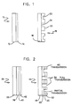
- FIGURE 1 there is shown a mask blank 10 having a transparent carrier 12 such as synthetic fused silica or any material substantially transparent to the wavelength of electromagnetic radiation being used. It should be understood that a certain amount of radiation is reflected any time such radiation is caused to be transmitted across a discontinuity in refractive index. Disposed on the carrier 12 is dielectric coating 14, commonly referred to as dielectric, such as disclosed in aforementioned co-pending patent application,application no. 87 113 673.5,which is herein incorporated by reference. The coating 14 is opaque to electromagnetic radiation. The coating 14 is a series of thin layers, each having a thickness of 1/4 the wavelength of the radiation in the medium being used.
- any arbitrarily high level of reflectivity can be obtained.
- the coating 14 can be disposed on the carrier 12 by means of electron beam deposition or by any other method known in the art. Intermediate layers of material may also be required between these thin layers to neutralize the effect of thermal and mechanical stress.
- a mask 16 Adjacent to the mask blank 10 in FIGURE 1 is a mask 16 fabricated and ready for use in optical or electromagnetic radiation lithography.
- the mask 16 has a carrier 18 that is chosen so that essentially all of the radiation impinging thereon is transmitted therethrough.
- Dielectric material disposed on the carrier 18 is made of a substance that reflects light or other electromagnetic radiation either totally or by a percentage of totality.
- the portion of the dielectric shown at reference numeral 20 disposed on the carrier 18 reflects all laser radiation impinging thereon.
- the portion of the dielectric shown at reference numeral 22 allows a percentage of laser radiation (e.g., 308 nm wavelength) to be transmitted through it and through the carrier 18.
- the reflectivity of the dielectric material at reference numeral 22 is 33.4%. Derivation of this percentage value is shown hereinbelow with reference to FIGURE 6.
- Tables of etch rate versus fluence curves are available for determining the reflectivity of specified portions of the mask 16 in order to etch certain material at a specified rate while etching another material at a second rate.
- Such curves for polyimides are published, for example, by J. H. Brannon, J. R. Lankard, A. I. Baise, F. Burns and J. Kaufman, in the Journal of Applied Physics 58(5), 1 Sept. 1985, pp 2036 - 2043. It can be seen that radiation impinging on the part of the carrier 18 on which no dielectric material exists 24 will not be reflected therefrom.
- the word reflective is a function of the electromagnetic radiation that is used in the system.
- one material may be reflective for one part of the spectrum, (e.g., visible light)
- another material may be reflective for another part of the spectrum (e.g., ultraviolet light).
- personality area or pattern of the mask 16 refers to any area thereof which transmits less light than the carrier 12 at the operating wavelength of a laser.
- Select area or pattern of the mask 16 refers to any area thereof which transmits a predetermined specified amount of light which is less than the amount of light transmitted by the carrier 12 at the operating wavelength of a laser but more light than does the full thickness dielectric 14.
- the select area is a portion of the personality area of the mask 16.
- a complement of the personality area is that area on a carrier not part of the personality area.
- creating the mask 16 requires the following procedure.
- To fabricate the personality areas obtain a carrier 18 with appropriate transmission properties Coat the carrier 18 with a dielectric material 20 which is totally reflecting at the operating wavelength of a predetermined laser.
- the dielectric 20 should be resistant to high fluence at the operating wavelength of the laser.
- select areas To fabricate the select areas, apply, bake, expose and develop a predetermined select pattern in a photoresist, not shown. Ion mill the dielectric 22 in the select pattern areas until the dielectric has the desired transmission characteristics at the operating wavelength of the laser. Strip the photoresist. Clean.
- the mask 16 can be fabricated by performing the following steps. Obtain a carrier 18 with appropriate transmission properties. Coat the carrier 18 with a dielectric material 20 which is totally reflecting at the operating wavelength of the laser. Apply, bake, expose and develop the predetermined personality pattern in a photoresist, not shown. Ion mill the exposed dielectric until the transmission of the remaining dielectric 22 is 1 - T, where T is the transmission desired for the select areas. Strip the photoresist. Apply, bake, expose and develop the predetermined select pattern in a second photoresist, not shown. Ion mill the exposed dielectric 24, which had been previously milled in the aforementioned ion mill step, to the base carrier 18. All the dielectric is removed from the areas etched in the aforementioned ion milling step. Sufficient dielectric will have been removed from the select areas 22 so that the transmission characteristic in the select areas is that which is desired. Strip the photoresist. Clean.
- a mask blank 34 has a carrier 36 on which is deposited a first material 38 that is partially reflective. Deposited on that first layer 38 is a layer of metal (e.g., chromium) 40. Adjacent to the metal layer 40 is a third layer 42 of totally reflective dielectric material.
- metal e.g., chromium
- the mask assembly 44 Adjacent to the mask blank 34 is a fabricated mask assembly ready for use in lithography and shown generally at reference numeral 44.
- the mask assembly 44 has a carrier 46, a first layer of material 48 covering at least a portion thereof, a second layer of material 50 covering at least a portion of the first layer 48 and a third layer of material 52 covering the second layer of material 50 where it exists.
- the material with a lower reflectivity 48 would normally be adjacent to the carrier 46 while the material with the higher reflectivity percentage 52 would be furthest from the carrier 46.
- Part of the first layer 48 is absent as are portions of the second and third layers 50, 52. In certain locations 54 no dielectric is on the carrier 46.
- Creating the mask 44 having a plurality of layers requires the following procedure.
- the first layer 48 is adjacent to the carrier 46. It is a dielectric which has partial transmission at the operating wavelength of a laser to be subsequently used.
- the second thin layer 50 is metal such as chromium or aluminum.
- the third layer 52 is a totally reflecting dielectric at the operating wavelength of the laser. Apply, bake, expose and develop a predetermined personality pattern in a photoresist, not shown. Ion mill the totally reflecting dielectric layer 52, etch the metal layer 50 and ion mill the partial transmission dielectric 48 to expose the carrier 46. Strip the photoresist. Apply, bake, expose and develop a predetermined select pattern in a photoresist. Ion mill the totally reflecting dielectric layer 52 and etch the metal layer 50. Strip the photoresist. Clean.
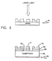
- FIGURE 3 there is shown a schematic representation of electromagnetic radiation impinging on a mask 16 and on portions of a metallized substrate 60 aligned therewith.
- the substrate 60 is one that has already been etched in accordance with the present invention using a mask 16 such as was hereinabove described with reference to FIGURE 1.
- the substrate 60 consists of a base 64 such as ceramic, on which is disposed a first layer of material 66 such as chromium, in the preferred embodiment.
- a second layer 68 such as copper, is disposed on the first layer 66.
- a third layer of material 70 such as chromium covers the second layer 68. After etching is complete, portions of the substrate 72 are not covered by any of the additional layers of material 66-70.
- a mask 16 for use in differential metal etching should allow the following processes to be conducted simultaneously:
- Process (a) is accomplished in accordance with the method disclosed in United States patents 4,490,210 and 4,490,211 issued to Chen et al, assigned to the present assignee and hereby incorporated by reference.
- a chlorine pressure and laser repetition rate must be chosen, in addition to a light wavelength and etch rate (fluence).
- the bottom Cr layer 66 is essentially vaporized once the Cu layer 68 is etched.
- the etch rate of the Cr-Cu-Cr is determined essentially by the etch rate of the top Cr layer 70 and the Cu layer 68 alone.
- the rate for select etching can be determined.
- a mask would be constructed as follows. Those regions of Cr-Cu-Cr which are not to be etched have corresponding totally reflecting areas on the mask. The areas of the mask that correspond to regions of the Cr-Cu-Cr where all the metal is to be removed are bare synthetic fused silica substrate without coating. The areas of the mask which correspond to select etching have a dielectric coating which is 45.3% reflective. If sufficient fluence is incident uniformly over the mask so that the fluence delivered on the metal in the personality etching areas is 384 mJ/cm2, personality and select etching is accomplished simultaneously and is completed concurrently.
- the ceramic base 64 is resistant to laser damage, the calculated reflectance in the areas of the mask which correspond to select etching can actually be considered a lower bound. Any reflectivity greater than the calculated reflectivity for the select areas can be used as long as the fluence delivered to the select areas is above the threshold needed for select etching under the given conditions. If the reflectivity in the select areas is greater than the calculated value, it will be necessary to overetch in the personality etching areas. Since the ceramic 64 is resistant to laser damage, overetching in the personality region causes few problems. The reflectivity in the select areas should never be less than the calculated values because overetching occurs in the select areas and considerable Cu can be lost therefrom.
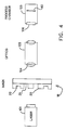
- FIGURE 4 there is shown a cross-sectional schematic diagram of apparatus for use in the method of the present invention.
- a laser 101 is positioned so as to form an optical line with a mask 16, an optical imaging system 103 and metallized base 60 to be etched.
- the base 60 is mounted in a reaction chamber 105.
- Laser 101 is a rare gas halide laser which is capable of emitting a characteristic wavelength which matches the absorption wavelength of the reaction product or the underlying material.
- One commercially available laser for purposes of this invention the LAMBDA PHYSIC EMG 201 model.
- the mask 16 is transparent to the laser light in the region 24 where there is no dielectric, is opaque in the region 20, and is partially transparent in the region 22 where the dielectric is present. As a result, light from laser 101 is transmitted by the mask 16 in the pattern corresponding to the transparent and partially transparent regions thereof.
- the imaging system 103 consists of at least one synthetic fused silica lens 104.
- the imaging system 103 images the patterned beam of laser radiation emerging from mask 16 onto the metallized base 60 for etching in conformance with the patterned laser beam.
- etching system shown in FIGURE 4 uses an image projection system 103 to effectively project the patterned beam of laser radiation onto the base 60, it is possible to dispense with the image system 103 when no volatile product is to be created (e.g., in the case of exposing, not etching, a photosensitive polymer) if a contact mask, placed in close proximity to the base 60, were utilized.
- the reaction chamber 105 is a conventional vacuum chamber constructed from stainless steel. It has removable vacuum flanges, not shown, on each of four openings. One of the flanges is connected to a pump, not shown. The pump provides the necessary low pressure within the reaction chamber 105 during the etching process. One of the other flanges is provided with a window 106 for permitting laser light to enter the chamber 105. The window 106 is optically clear and distortion-free to ensure that the mask image projected thereon is transmitted without distortion to the base 60. One of the other flanges of the reaction chamber 105 is also provided with a tube, not shown, to permit introduction of reactive gas into the chamber 105. Suitable means, such as a sample holder, not shown, is mounted in the chamber 105 to accommodate the base 60 to be etched.
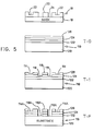
- FIGURE 5 there is shown a series of schematic representations of a substrate 119 being etched to three different levels successively over a period of time in accordance with the present invention.
- the mask assembly 16 has a layer of dielectric material disposed on a carrier 18.
- the first thin portion of the dielectric 22 covers at least part of the carrier 18 and the thicker portion of the dielectric 20 covers at least part of the thin portion 22.
- the base 120 of the substrate 119 has three complete, unetched layers disposed thereon: the first layer 122 being chromium; the second layer 124 being copper; and the uppermost layer 126 being chromium in the preferred multi-layer embodiment.
- laser light not shown, passes through the mask 16 under appropriate conditions and in conjunction with the process chamber 105 (FIGURE 4) as hereinabove described, etching begins.
- time T-1 portions of the uppermost two layers 124 and 126 are etched and removed. It can be seen that the central portions 118 are etched faster than a portion 114 of the top layer 126. This is due to the fact that the mask 16 has totally reflective and partially reflective portions corresponding to positions on the substrate 119. The absence of dielectric 24 on the mask 16 corresponds to the fastest etching areas 118 of the layers 122-126 of the substrate 119. Similarly, presence of the thickest portion of dielectric 20 of the mask 16 results in no etching of the corresponding location 116 on the substrate 119. The thin, and therefore partially reflective portion of dielectric 22 of the mask 16 results in etching only the top layer 126 of the substrate 119 corresponding to a position shown as reference numeral 114.
- FIGURE 6 there is shown a cross-sectional isometric view of a substrate 130 comprising a substantially uniform block of etchable polymer such as polyimide.
- the three dimensional view of the substrate 130 produced in accordance with the aforementioned method of the present invention is helpful in understanding the value of differential etching.
- the upper surface of the polyimide 130 is shown at reference numeral 131.
- Surface features 132, 134, 136 and 138 have been etched to varying depths by the use of a laser system.
- the features shown as reference numerals 132 and 136 represent viaduct holes or vias.
- Hole 136 has been etched to a depth of H1.
- the rectilinear circuit line structure 134 has been etched to a greater depth, H2.
- a thru hole 138 connects the upper surface of substrate 130 to the lower surface thereof.
- the thru hole 138 has been etched entirely through the thickness of the substrate 130, referred to as thickness H3.
- a mask 16 (FIGURE 1) for use in polyimide differential etching should satisfy the following three criteria:
- the first step is to measure the etch rate of the polyimide of interest 130 in air at 308 nm.
- the etch rate data collected by Brannon et al, supra will be used.
- the etch rate versus fluence (energy per cm2) data follows a Beer-Lambert law.
- ⁇ is the polyimide absorption coefficient for 308 nm laser light
- ⁇ t is the threshold fluence for etching polyimide at wavelength 308 nm. Both ⁇ and ⁇ t are functions only of the material being etched and the wavelength of light being used.
- ER i is the etch depth per pulse of the polyimide 130 at fluence ⁇ i . Note that ⁇ i ⁇ ⁇ t for etching to occur.
- the reflective dielectric is completely removed from the area of the mask corresponding to the thru hole 138 on the polyimide 130. Reflection losses on other optical surfaces would attenuate light passing through all areas of the mask equally and would not affect the ratio of the etch rates.
- T1 0.955 and substituting into equation (11) results in a value for T2 of 0.666.
- the mask 16 is constructed such that certain areas 20 of the mask 16 are totally reflecting at wavelength 308 nm.
- areas 24 of the mask 16 which correspond to etching at 100 Nanometer/pulse all coatings are removed; only the synthetic fused silica substrate 18 remains.
- areas 22 of the mask 16 only a dielectric coating with reflectivity of 33.4% at wavelength 308 nm remains.
- the etch rate at reference numeral 134 is 60 Nanometer/pulse and no etching occurs at the surface 131.
- circuit boards or semiconductor features can be etched to varying depths simultaneously by the use of the present invention. It should be noted that, while three different depths of etching are shown in FIGURE 6, other depths can also be created by modifying the structure of the mask 16 (FIGURE 1) in a suitable manner. For example, any number of dielectric layers, with or without endpoint detection, can be fabricated in a mask which, in turn, can be used to manufacture a substrate.
Landscapes
- Engineering & Computer Science (AREA)
- Physics & Mathematics (AREA)
- Optics & Photonics (AREA)
- Computer Hardware Design (AREA)
- Microelectronics & Electronic Packaging (AREA)
- Power Engineering (AREA)
- Condensed Matter Physics & Semiconductors (AREA)
- General Physics & Mathematics (AREA)
- Manufacturing & Machinery (AREA)
- High Energy & Nuclear Physics (AREA)
- Ceramic Engineering (AREA)
- Electromagnetism (AREA)
- Health & Medical Sciences (AREA)
- Toxicology (AREA)
- Plasma & Fusion (AREA)
- Mechanical Engineering (AREA)
- ing And Chemical Polishing (AREA)
- Preparing Plates And Mask In Photomechanical Process (AREA)
Claims (6)
- Procédé pour effectuer une attaque différentielle d'un substrat (119) constitué d'un corps (120) comportant un revêtement (122, ...) par un faisceau de rayonnement électromagnétique, comprenant les étapes suivantes:a) fourniture d'un masque du type comprenant un support (18) sensiblement transparent à un faisceau de rayonnement électromagnétique et recouvert d'un revêtement configuré (20, ...), dans lequel ledit revêtement configuré comporte au moins trois régions (22, 24, ...) ayant un pouvoir de réflexion différent,b) éclairage dudit substrat par un faisceau à travers ledit masque, et caractérisé parc) le réglage de la densité d'énergie locale dudit faisceau de telle sorte que des zones déterminées du revêtement correspondant auxdites régions sont attaquées chacune selon une profondeur d'attaque différente pré-sélectionnée (H1, H2, ..., H3) pendant le même temps.
- Procédé selon la revendication 1, dans lequel l'attaque est effectuée en présence d'un gaz réactif sélectionné.
- Procédé selon la revendication 1 ou 2, dans lequel ledit revêtement comporte au moins deux couches qui diffèrent dans la composition du matériau.
- Procédé selon une revendication 1, 2 ou 3, dans lequel ledit revêtement à attaquer comporte trois couches consistant en une couche inférieure de Cr, une couche intermédiaire de Cu et une couche supérieure de Cr.
- Procédé selon l'une quelconque des revendications 1 à 4, dans lequel le faisceau de rayonnement est généré par un laser excimer.
- Procédé selon la revendication 1 dans lequel le revêtement à attaquer est sélectionné parmi un groupe consistant en métaux, polymères, et semiconducteurs.
Applications Claiming Priority (2)
| Application Number | Priority Date | Filing Date | Title |
|---|---|---|---|
| US924487 | 1986-10-29 | ||
| US06/924,487 US4684436A (en) | 1986-10-29 | 1986-10-29 | Method of simultaneously etching personality and select |
Publications (3)
| Publication Number | Publication Date |
|---|---|
| EP0265872A2 EP0265872A2 (fr) | 1988-05-04 |
| EP0265872A3 EP0265872A3 (en) | 1990-04-25 |
| EP0265872B1 true EP0265872B1 (fr) | 1995-03-08 |
Family
ID=25450260
Family Applications (1)
| Application Number | Title | Priority Date | Filing Date |
|---|---|---|---|
| EP87115596A Expired - Lifetime EP0265872B1 (fr) | 1986-10-29 | 1987-10-23 | Gravure simultanée de la structure multicouche et de la structure d'image |
Country Status (4)
| Country | Link |
|---|---|
| US (1) | US4684436A (fr) |
| EP (1) | EP0265872B1 (fr) |
| JP (1) | JPS63111187A (fr) |
| DE (1) | DE3751134T2 (fr) |
Families Citing this family (37)
| Publication number | Priority date | Publication date | Assignee | Title |
|---|---|---|---|---|
| US5179262A (en) * | 1986-10-14 | 1993-01-12 | Allergan, Inc. | Manufacture of ophthalmic lenses by excimer laser |
| US4684436A (en) * | 1986-10-29 | 1987-08-04 | International Business Machines Corp. | Method of simultaneously etching personality and select |
| JPS63234548A (ja) * | 1987-03-24 | 1988-09-29 | Oki Electric Ind Co Ltd | 半導体素子の製造方法 |
| US5354695A (en) | 1992-04-08 | 1994-10-11 | Leedy Glenn J | Membrane dielectric isolation IC fabrication |
| CA2021110A1 (fr) * | 1989-09-05 | 1991-03-06 | Colloptics, Inc. | Sculpture ou rayons laser avec cache de surface pour modelage |
| GB9008580D0 (en) * | 1990-04-17 | 1990-06-13 | Pilkington Diffractive Lenses | Manufacture of contact lenses |
| US5213916A (en) * | 1990-10-30 | 1993-05-25 | International Business Machines Corporation | Method of making a gray level mask |
| US5148319A (en) * | 1991-02-25 | 1992-09-15 | Hughes Aircraft Company | System for fabricating micro optical elements |
| US6714625B1 (en) | 1992-04-08 | 2004-03-30 | Elm Technology Corporation | Lithography device for semiconductor circuit pattern generation |
| FR2694131B1 (fr) * | 1992-07-21 | 1996-09-27 | Balzers Hochvakuum | Procede et installation pour la fabrication d'un composant, notamment d'un composant optique, et composant optique ainsi obtenu. |
| US5498850A (en) * | 1992-09-11 | 1996-03-12 | Philip Morris Incorporated | Semiconductor electrical heater and method for making same |
| US5539175A (en) * | 1994-03-21 | 1996-07-23 | Litel Instruments | Apparatus and process for optically ablated openings having designed profile |
| US5501925A (en) * | 1994-05-27 | 1996-03-26 | Litel Instruments | High power masks and methods for manufacturing same |
| TW366367B (en) * | 1995-01-26 | 1999-08-11 | Ibm | Sputter deposition of hydrogenated amorphous carbon film |
| US5591480A (en) * | 1995-08-21 | 1997-01-07 | Motorola, Inc. | Method for fabricating metallization patterns on an electronic substrate |
| JPH09207343A (ja) * | 1995-11-29 | 1997-08-12 | Matsushita Electric Ind Co Ltd | レーザ加工方法 |
| US5915167A (en) | 1997-04-04 | 1999-06-22 | Elm Technology Corporation | Three dimensional structure memory |
| US6551857B2 (en) | 1997-04-04 | 2003-04-22 | Elm Technology Corporation | Three dimensional structure integrated circuits |
| US6080959A (en) * | 1999-03-12 | 2000-06-27 | Lexmark International, Inc. | System and method for feature compensation of an ablated inkjet nozzle plate |
| US6495239B1 (en) * | 1999-12-10 | 2002-12-17 | International Business Corporation | Dielectric structure and method of formation |
| US6834423B2 (en) * | 2000-07-31 | 2004-12-28 | Canon Kabushiki Kaisha | Method of manufacturing a liquid discharge head |
| TW449929B (en) * | 2000-08-02 | 2001-08-11 | Ind Tech Res Inst | Structure and manufacturing method of amorphous-silicon thin film transistor array |
| US6748994B2 (en) | 2001-04-11 | 2004-06-15 | Avery Dennison Corporation | Label applicator, method and label therefor |
| US6677552B1 (en) | 2001-11-30 | 2004-01-13 | Positive Light, Inc. | System and method for laser micro-machining |
| AU2003255254A1 (en) | 2002-08-08 | 2004-02-25 | Glenn J. Leedy | Vertical system integration |
| US7645300B2 (en) | 2004-02-02 | 2010-01-12 | Visiogen, Inc. | Injector for intraocular lens system |
| US20080182179A1 (en) * | 2007-01-25 | 2008-07-31 | Allied Integrated Patterning Corp. | Gray tone mask and method for manufacturing the same |
| US8008209B2 (en) * | 2007-10-24 | 2011-08-30 | International Business Machines Corporation | Thermal gradient control of high aspect ratio etching and deposition processes |
| EP3309823B1 (fr) * | 2008-09-18 | 2020-02-12 | FUJIFILM SonoSite, Inc. | Transducteurs à ultrasons |
| US9173047B2 (en) | 2008-09-18 | 2015-10-27 | Fujifilm Sonosite, Inc. | Methods for manufacturing ultrasound transducers and other components |
| US9184369B2 (en) | 2008-09-18 | 2015-11-10 | Fujifilm Sonosite, Inc. | Methods for manufacturing ultrasound transducers and other components |
| DE102008058535A1 (de) * | 2008-11-21 | 2010-05-27 | Tesa Se | Verfahren zur Materialbearbeitung mit energiereicher Strahlung |
| US20110115047A1 (en) * | 2009-11-13 | 2011-05-19 | Francois Hebert | Semiconductor process using mask openings of varying widths to form two or more device structures |
| US8633115B2 (en) * | 2011-11-30 | 2014-01-21 | Applied Materials, Inc. | Methods for atomic layer etching |
| US20160074968A1 (en) * | 2014-09-11 | 2016-03-17 | Suss Microtec Photonic Systems Inc. | Laser etching system including mask reticle for multi-depth etching |
| US9730625B2 (en) | 2015-03-02 | 2017-08-15 | Verily Life Sciences Llc | Automated blood sampling device |
| US10765361B2 (en) | 2015-03-02 | 2020-09-08 | Verily Life Sciences Llc | Automated sequential injection and blood draw |
Citations (3)
| Publication number | Priority date | Publication date | Assignee | Title |
|---|---|---|---|---|
| FR2228242A1 (fr) * | 1973-05-03 | 1974-11-29 | Ibm | |
| US4374911A (en) * | 1978-04-28 | 1983-02-22 | International Business Machines Corporation | Photo method of making tri-level density photomask |
| EP0120834A1 (fr) * | 1983-03-01 | 1984-10-03 | Österreichisches Forschungszentrum Seibersdorf Ges.m.b.H. | Filtres optiques texturés et procédé de fabrication |
Family Cites Families (12)
| Publication number | Priority date | Publication date | Assignee | Title |
|---|---|---|---|---|
| US2841477A (en) * | 1957-03-04 | 1958-07-01 | Pacific Semiconductors Inc | Photochemically activated gaseous etching method |
| US3649393A (en) * | 1970-06-12 | 1972-03-14 | Ibm | Variable depth etching of film layers using variable exposures of photoresists |
| US3823015A (en) * | 1973-01-02 | 1974-07-09 | Collins Radio Co | Photo-masking process |
| US4035522A (en) * | 1974-07-19 | 1977-07-12 | International Business Machines Corporation | X-ray lithography mask |
| US4151072A (en) * | 1977-05-16 | 1979-04-24 | Phillips Petroleum Company | Reclaiming used lubricating oils |
| JPS55145178A (en) * | 1979-05-02 | 1980-11-12 | Agency Of Ind Science & Technol | Precision working method of solid surface |
| JPS57121226A (en) * | 1981-01-21 | 1982-07-28 | Hitachi Ltd | Photo mask |
| US4331504A (en) * | 1981-06-25 | 1982-05-25 | International Business Machines Corporation | Etching process with vibrationally excited SF6 |
| US4508749A (en) * | 1983-12-27 | 1985-04-02 | International Business Machines Corporation | Patterning of polyimide films with ultraviolet light |
| US4490210A (en) * | 1984-01-24 | 1984-12-25 | International Business Machines Corporation | Laser induced dry chemical etching of metals |
| US4490211A (en) * | 1984-01-24 | 1984-12-25 | International Business Machines Corporation | Laser induced chemical etching of metals with excimer lasers |
| US4684436A (en) * | 1986-10-29 | 1987-08-04 | International Business Machines Corp. | Method of simultaneously etching personality and select |
-
1986
- 1986-10-29 US US06/924,487 patent/US4684436A/en not_active Expired - Lifetime
-
1987
- 1987-05-15 JP JP62117268A patent/JPS63111187A/ja active Granted
- 1987-10-23 EP EP87115596A patent/EP0265872B1/fr not_active Expired - Lifetime
- 1987-10-23 DE DE3751134T patent/DE3751134T2/de not_active Expired - Fee Related
Patent Citations (3)
| Publication number | Priority date | Publication date | Assignee | Title |
|---|---|---|---|---|
| FR2228242A1 (fr) * | 1973-05-03 | 1974-11-29 | Ibm | |
| US4374911A (en) * | 1978-04-28 | 1983-02-22 | International Business Machines Corporation | Photo method of making tri-level density photomask |
| EP0120834A1 (fr) * | 1983-03-01 | 1984-10-03 | Österreichisches Forschungszentrum Seibersdorf Ges.m.b.H. | Filtres optiques texturés et procédé de fabrication |
Also Published As
| Publication number | Publication date |
|---|---|
| US4684436A (en) | 1987-08-04 |
| DE3751134D1 (de) | 1995-04-13 |
| JPS6411717B2 (fr) | 1989-02-27 |
| EP0265872A2 (fr) | 1988-05-04 |
| EP0265872A3 (en) | 1990-04-25 |
| DE3751134T2 (de) | 1995-09-14 |
| JPS63111187A (ja) | 1988-05-16 |
Similar Documents
| Publication | Publication Date | Title |
|---|---|---|
| EP0265872B1 (fr) | Gravure simultanée de la structure multicouche et de la structure d'image | |
| JP2538728B2 (ja) | グレイ・レベル・マスクおよびその製造方法 | |
| KR100231937B1 (ko) | 멀티레벨 레티클 시스템 및 멀티레벨 포토레지스트 프로파일 형성 방법 | |
| EP0383534A2 (fr) | Masque optique, procédé de fabrication et méthode d'exposition avec ce masque | |
| US5506080A (en) | Lithographic mask repair and fabrication method | |
| EP0493963A1 (fr) | Masque microstructuré ayant une couche transparente d'arrêt de gravure | |
| EP1321820B1 (fr) | Photomasque a decalage de phase a demi-ton et ebauche de photomasque a decalage de phase a demi-ton | |
| US5686206A (en) | Method for the repair of lithographic masks | |
| US5695896A (en) | Process for fabricating a phase shifting mask | |
| EP0134789B1 (fr) | Systeme de reserve a deux niveaux pour lumiere ultraviolette pour la gravure de motifs sur des substrats a degre eleve de reflexion | |
| EP1116998B1 (fr) | Ebauche pour masque à décalage de phase atténué et masque correspondant | |
| KR100306861B1 (ko) | 포토마스크블랭크및위상쉬프트포토마스크 | |
| US6368775B1 (en) | 3-D photo-patterning of refractive index structures in photosensitive thin film materials | |
| US4144066A (en) | Electron bombardment method for making stained glass photomasks | |
| JP3645888B2 (ja) | ハーフトーン型位相シフトマスク | |
| JPH0627636A (ja) | フォトマスク及びフォトマスクの製造方法及びエッチング方法及び露光方法 | |
| US5543252A (en) | Method for manufacturing exposure mask and the exposure mask | |
| US5935734A (en) | Method for fabrication of and apparatus for use as a semiconductor photomask | |
| EP1143295B1 (fr) | Masque à décalage de phase atténué ainsi que précurseurs pour celui-ci et un procédé pour la réalisation de motifs utilisant ce masque | |
| US5756236A (en) | Fabrication of high resolution aluminum ablation masks | |
| US5468576A (en) | Method for manufacturing exposure mask | |
| EP0162717B1 (fr) | Procédé pour obtenir des modèles de masques | |
| GB2088084A (en) | Pattern Exposure Mask | |
| JP3225074B2 (ja) | 位相シフトフォトマスクの製造方法 | |
| JP3257130B2 (ja) | エッジ強調型位相シフトマスクの製造方法 |
Legal Events
| Date | Code | Title | Description |
|---|---|---|---|
| PUAI | Public reference made under article 153(3) epc to a published international application that has entered the european phase |
Free format text: ORIGINAL CODE: 0009012 |
|
| AK | Designated contracting states |
Kind code of ref document: A2 Designated state(s): DE FR GB IT |
|
| 17P | Request for examination filed |
Effective date: 19880823 |
|
| PUAL | Search report despatched |
Free format text: ORIGINAL CODE: 0009013 |
|
| AK | Designated contracting states |
Kind code of ref document: A3 Designated state(s): DE FR GB IT |
|
| 17Q | First examination report despatched |
Effective date: 19920617 |
|
| GRAA | (expected) grant |
Free format text: ORIGINAL CODE: 0009210 |
|
| AK | Designated contracting states |
Kind code of ref document: B1 Designated state(s): DE FR GB IT |
|
| PG25 | Lapsed in a contracting state [announced via postgrant information from national office to epo] |
Ref country code: IT Free format text: LAPSE BECAUSE OF FAILURE TO SUBMIT A TRANSLATION OF THE DESCRIPTION OR TO PAY THE FEE WITHIN THE PRE;WARNING: LAPSES OF ITALIAN PATENTS WITH EFFECTIVE DATE BEFORE 2007 MAY HAVE OCCURRED AT ANY TIME BEFORE 2007. THE CORRECT EFFECTIVE DATE MAY BE DIFFERENT FROM THE ONE RECORDED.SCRIBED TIME-LIMIT Effective date: 19950308 |
|
| REF | Corresponds to: |
Ref document number: 3751134 Country of ref document: DE Date of ref document: 19950413 |
|
| ET | Fr: translation filed | ||
| PGFP | Annual fee paid to national office [announced via postgrant information from national office to epo] |
Ref country code: FR Payment date: 19951009 Year of fee payment: 9 |
|
| PGFP | Annual fee paid to national office [announced via postgrant information from national office to epo] |
Ref country code: DE Payment date: 19951030 Year of fee payment: 9 |
|
| PLBE | No opposition filed within time limit |
Free format text: ORIGINAL CODE: 0009261 |
|
| STAA | Information on the status of an ep patent application or granted ep patent |
Free format text: STATUS: NO OPPOSITION FILED WITHIN TIME LIMIT |
|
| 26N | No opposition filed | ||
| PGFP | Annual fee paid to national office [announced via postgrant information from national office to epo] |
Ref country code: GB Payment date: 19960925 Year of fee payment: 10 |
|
| PG25 | Lapsed in a contracting state [announced via postgrant information from national office to epo] |
Ref country code: FR Effective date: 19970630 |
|
| PG25 | Lapsed in a contracting state [announced via postgrant information from national office to epo] |
Ref country code: DE Effective date: 19970701 |
|
| REG | Reference to a national code |
Ref country code: FR Ref legal event code: ST |
|
| PG25 | Lapsed in a contracting state [announced via postgrant information from national office to epo] |
Ref country code: GB Free format text: LAPSE BECAUSE OF NON-PAYMENT OF DUE FEES Effective date: 19971023 |
|
| GBPC | Gb: european patent ceased through non-payment of renewal fee |
Effective date: 19971023 |