EP0120194B1 - Speicherprogrammierbare Steuerung mit Wort- und Bitprozessor - Google Patents
Speicherprogrammierbare Steuerung mit Wort- und Bitprozessor Download PDFInfo
- Publication number
- EP0120194B1 EP0120194B1 EP84100397A EP84100397A EP0120194B1 EP 0120194 B1 EP0120194 B1 EP 0120194B1 EP 84100397 A EP84100397 A EP 84100397A EP 84100397 A EP84100397 A EP 84100397A EP 0120194 B1 EP0120194 B1 EP 0120194B1
- Authority
- EP
- European Patent Office
- Prior art keywords
- word
- processor
- bit
- programme
- address
- Prior art date
- Legal status (The legal status is an assumption and is not a legal conclusion. Google has not performed a legal analysis and makes no representation as to the accuracy of the status listed.)
- Expired
Links
Images
Classifications
-
- G—PHYSICS
- G05—CONTROLLING; REGULATING
- G05B—CONTROL OR REGULATING SYSTEMS IN GENERAL; FUNCTIONAL ELEMENTS OF SUCH SYSTEMS; MONITORING OR TESTING ARRANGEMENTS FOR SUCH SYSTEMS OR ELEMENTS
- G05B19/00—Program-control systems
- G05B19/02—Program-control systems electric
- G05B19/04—Program control other than numerical control, i.e. in sequence controllers or logic controllers
- G05B19/05—Programmable logic controllers, e.g. simulating logic interconnections of signals according to ladder diagrams or function charts
- G05B19/052—Linking several PLC's
Definitions
- Programmable logic controllers are described in more detail, for example, in Siemens magazine “Energietechnik” 1979, number 2, pages 43 to 47 or in number 4, pages 136 to 139 or in European patent specification 10 170 and US patent specifications 3 921 146 or 3 942158 .
- word processors are generally intended for a wide range of users in their instruction set, i.e. universal, designed. In the course of development, this set of commands increases in scope and performance. It is also characteristic of this development that more and more information carriers (bits) are combined and processed in parallel.
- peripheral states e.g. "On” switch, "Off” switch, input condition met or not met.
- a convenient, programmable logic controller of the type mentioned at the outset is intended to perform both logical linking of bit-wide data and complex functions with word-wide data, such as Can perform arithmetic function, data transfer, timing, etc.
- the object of the present invention is to provide a simple coupling and synchronization of the two processors, in which one is largely independent of the type of word processor.
- the bit processor controls that address in the mapping memory which contains the start address at which a routine for processing the breakpoint in the operating system of the word processor begins.
- the execution of the binary instructions is transferred to a separate fast bit processor 3, whereas a relatively slow word processor 2 carries out the complex functions.
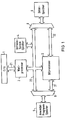
- the word processor 2 has a peripheral bus to which the input and output modules 1 are connected to and from the process, furthermore an internal system bus 22, to the operating system memory 4 and to data switches 8 An Turner program memory 5 and data memory 6 with a process image can be connected.
- the bit processor 3 is also connected to the same bus 22 and has exclusive access to user program memory 5 and data memory 6 with process image via its own buses 31 and 32 and via data switches 8.
- the traffic with the periphery always runs via the word processor 2, which at the cycle boundaries always stores the state of all input information from the process into the internal data memory 6 and transmits the output signals resulting from the links in the data memory 6 to the process periphery at the end of the cycle.
- the actual signals of the process peripherals are not used, but the internal process image in the data memory 6 is used (see, for example, European Patent 10170).
- the instructions about bit or word operations are encrypted in a special programming language and stored in the user program memory 5. These instructions are processed directly by the bit processor 3 and in certain program parts by the word processor 2. These program parts and the routine mentioned at the outset are fixed in the operating system memory 4 of the word processor 2 in the language of the microprocessor used.
- the bit processor 3 itself behaves like a memory interface or an intelligent peripheral module for the word processor 2. It has internal registers from which the word processor 2 can keep the current status at any time, e.g. "RUN” or "HALT". The bit processor 3 can also be started or stopped by the word processor 2 at any time by write access to one of these registers.
- the program counter for the actual program sequence lies in the bit processor 3. This, after it has been started, fetches instructions D from the program memory 5 and differentiates them according to word and bit operations. After recognizing a bit operation, he immediately executes it himself, if a word operation is recognized, he transfers it to word processor 2 and automatically goes into the “HALT” status.
- the bit processor 3 itself has no access or control to the word processor 2. It merely provides information for the word processor 2 in its internal registers. The control of the overall system must therefore start from the word processor 2. This principle ensures that the bit processor does not have to be tailored to a specific word processor type, but rather is kept general in its interface and can be handled by any standard microprocessor such as a memory or an intelligent peripheral module.
- the tasks of the bit processor 3 thus consist of fetching command D in the user program memory 5 at the address A of its program counter, recognizing the type of command (word or bit operation) and then reacting accordingly. This means that in the case of bit operations, these are processed by the bit processor, while when a word operation is recognized, it is passed on to the word processor 2, whereupon the bit processor then stops and waits for the word processor to start again.
- the tasks of the word processor 2 consist of processing certain routines, both asynchronous and time-controlled, and additionally controlling the bit processor 3 with processing word operations recognized by the bit processor in special program parts.
- Each word operation is interpreted by the word processor 2 by a special program part.
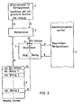
- the word processor 2 receives the entry address into the program part assigned to a specific operation not directly via the code of the word operation in the user program memory 5, but via an interposed mapping memory 9.
- the code of the word operation forms the address A1 for a specific memory cell of the memory 9, below which is entered as the date D1 the entry address in the corresponding program part.
- the word processor can then also access further data in the user program memory. In this way it is achieved that the entry addresses of the assigned program parts can be kept variable with a fixed command code of the word operation.
- the synchronization between the word processor and the bit processor is carried out by the word processor 2 by means of the STOP / start control of the bit processor.
- the program counter of the bit processor 3 can be read and written by the word processor 2. If the program counter has been preset with a defined value by the word processor, the bit processor 3 is started. The bit processor 3 starts up freely and takes over the aforementioned tasks.
- the word processor 2 either processes routines occurring parallel to the bit processor 3 or is in an idle loop (poll loop) in which it only addresses two successive 8-bit registers 31 of the bit processor 3, whereupon these registers 31 of the bit processor 3 carry out the mapping - Activate memory 9 in this way, ie address that this puts data D1 corresponding to the type of word operation on the data bus.
- This data is interpreted as a 16-bit address A2, to which the word processor 3 now branches.
- This address A2 is either the entry address for one of the program parts for word operations or the beginning of this idle loop itself.
- these registers 31 supply the basic address AO of the mapping memory 9, i.e. the entry or start address of the poll loop. If the bit processor 3 detects a word operation in the user program memory 5, it switches the mapping memory 9 to the mapping memory 9 via the correspondingly modified register 31, and the word processor reads the data D1 in its loop under the address of the abovementioned registers memory cell of the mapping memory 9 addressed by the bit processor 3, that is to say the entry address A2 into the program part D2 for this word operation in the memory 4. The word processor 2 therefore always branches to where the address in the bit processor in the above-mentioned registers 31 is pointing, that is to say Start of the loop or in one of the program parts.
- the bit processor 3 stops and must be restarted by the word processor 2 at the end of the corresponding program part of the word processor for the word operation. Since the program counter in the bit processor is incremented each time an instruction is completely fetched, it already receives the correct continuation address for further reading in the user program memory 5 .
- the polling loop of word processor 2 in conventional microprocessors consists of approx. 2 to 4 commands - address registers of the bit processor and jump to the address read from memory 9. This ensures an extremely short response time even when word operations are recognized.
- mapping memory 9 software-based branching via a list is superfluous due to the mapping memory 9, and this in turn saves time.
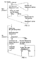
- the word processor 2 can jump from its poll loop into the asynchronous or time-controlled routines mentioned at the beginning via “interrupts” and these work in parallel with the work of the bit processor, as can also be seen from FIG. 3. If the bit processor 3 then recognizes a word operation, the actual program flow only remains until the word processor 2 has returned to its poll loop and can process the word operation.
- the main advantages of this coupling are the simple synchronization option between the word and bit processor, the possible parallel operation of both processors and the independence of the bit processor design from the type of word processor.
- the interface to the bit processor is implemented as a memory interface and is free of any additional control lines. However, a less complex and somewhat less efficient solution is also possible.
- the memory 9 is omitted.
- the memory content which transforms the number that specifies the type of the word command, to the entry address into the program part of the word command, is then located in the memory 4 in a constant data field.
- the word processor 2 reads in the bit processor only the information which indicates whether a word command has occurred, which word command is pending and whether a breakpoint has been reached.
- the required entry address is now programmed by accessing the table, i.e. the data field.
- the word processor 2 uses the information from the bit processor 3 directly as an entry address or forms this address from it with logical or arithmetic operations (masking, shifting, adding).
Landscapes
- General Physics & Mathematics (AREA)
- Engineering & Computer Science (AREA)
- Automation & Control Theory (AREA)
- Physics & Mathematics (AREA)
- Multi Processors (AREA)
- Communication Control (AREA)
- Programmable Controllers (AREA)
- Transceivers (AREA)
- Executing Machine-Instructions (AREA)
- Debugging And Monitoring (AREA)
- Devices For Executing Special Programs (AREA)
- Advance Control (AREA)
- Electrophonic Musical Instruments (AREA)
- Circuits Of Receivers In General (AREA)
- Input Circuits Of Receivers And Coupling Of Receivers And Audio Equipment (AREA)
- Stored Programmes (AREA)
Description
- Die Erfindung bezieht sich auf eine speicherprogrammierbare Steuerung mit zyklisch durchlaufenem Anwenderprogramm, bestehend zumindest aus:
- a) einem Wortprozessor zur Bearbeitung von Betriebssystem- und Wortbefehlen,
- b) einem Bitprozessor zur Bearbeitung binärer Verknüpfungsbefehle und
- c) Anwenderprogrammspeicher, Betriebssystemspeicher und Datenspeicher mit binärem Prozessabbild.
- Speicherprogrammierbare Steuerungen sind beispielsweise in der Siemens-Zeitschrift «Energietechnik» 1979, Heft 2, Seiten 43 bis 47 oder in Heft 4, Seiten 136 bis 139 oder in der europäischen Patentschrift 10 170 und den US-Patentschriften 3 921 146 oder 3 942158 näher beschrieben.
- Derzeit gängige Mikroprozessoren, im folgenden als Wortprozessoren bezeichnet, sind in ihrem Befehlssatz in der Regel für einen breiten Anwenderkreis, d.h. universell, ausgelegt. Im Zuge der Entwicklung nimmt dieser Befehlssatz an Umfang und Leistungsfähigkeit ständig zu. Kennzeichnend bei dieser Entwicklung ist auch, dass immer mehr Informationsträger (Bits) zusammengefasst und parallel bearbeitet werden.
- Es gibt jedoch auch spezielle Anwendungsfälle, bei denen weitgehend bitbreite Informationen bearbeitet werden müssen. Hierbei trägt z.B. ein Bit unabhängig von anderen die Information über periphere Zustände, wie z.B. Schalter «Ein», Schalter «Aus», Eingangsbedingung erfüllt oder nicht erfüllt.
- Eine komfortable, speicherprogrammierbare Steuerung der eingangs genannten Art soll sowohl logische Verknüpfung von bitbreiten Daten durchführen als auch komplexe Funktionen mit wortbreiten Daten, wie z.B. Arithmetikfunktion, Datentransfer, Zeitenbildung usw. ausführen können.
- Es ist daher vorteilhaft, im Rahmen einer speicherprogrammierbaren Steuerung ein Mehrprozessorsystem zu verwenden, bei dem die Ausführung der Binärbefehle einem gesonderten schnellen Bitprozessor übertragen wird, wogegen ein relativ langsamer Wortprozessor die komplexen Funktionen ausführen kann (vgl. z.B. Siemens-Zeitschrift Energietechnik 1980, Heft 9, Seiten 361).
- Da die wortbreite und bitbreite Verarbeitung der Daten gemischt und zum Teil abhängig voneinander stattfindet, ist ein spezielles Verfahren zur Kopplung und Synchronisation der Prozessoren erforderlich. Berücksichtigt werden muss dabei ausserdem, dass vom Wortprozessor, sowohl in bestimmten Abständen als auch völlig asynchrom zum eigentlichen Programmablauf (Wort-und Bitoperationen), zusätzlich spezielle Routinen abgearbeitet werden müssen. Der eigentliche Programmablauf mit bit- und wortweiser Datenbearbeitung soll durch diese Routinen möglichst wenig belastet werden, jedoch niedrigste Priorität haben, d.h. sobald die Bearbeitung einer dieser speziellen Routinen anfällt, muss diese sofort und unbedingt vorgenommen werden.
- Die Aufgabe der vorliegenden Erfindung besteht darin, eine einfache Kopplung und Synchronisation der beiden Prozessoren anzugeben, bei der man von der Art des Wortprozessors weitgehend unabhängig ist.
- Diese Aufgabe wird erfindungsgemäss durch die kennzeichnenden Merkmale des Hauptanspruches gelöst; eine besonders vorteilhafte Ausführung ergibt sich mit folgenden Merkmalen:
- a) dem Bitprozessor ist ein Mapping-Speicher mit Befehlsadressen zugeordnet, unter denen Programmroutinen des Wortprozessors beginnen,
- b) der Bitprozessor steuert beim Lesen und Abarbeiten eines binären Verknüpfungsbefehls des Anwenderprogrammspeichers eine Adresse des Mapping-Speichers an, unter der die Anfangsadresse einer Programmroutine des Wortprozessors zur fortlaufenden Abfrage des Mapping-Speichers steht (Poll-Schleife),
- c) der Bitprozessor steuert beim Lesen eines Wortbefehls im Anwenderprogrammspeicher diejenige Adresse im Mapping-Speicher an, unter der die Anfangsadresse der diesem Wortbefehl entsprechenden Programmroutine für den Wortprozessor gespeichert ist und geht bis zum Abarbeiten der Programmroutine in den Haltzustand, und der Wortprozessor springt nach der Abfrage der Anfangsadresse zu dieser Anfangsadresse.
- Ebenso steuert der Bitprozessor beim Erreichen eines Haltepunktes diejenige Adresse im Mapping-Speicher an, worin die Anfangsadresse steht, unter der eine Routine zur Bearbeitung des Haltepunktes im Betriebssystem des Wortprozessors beginnt.
- Auf die vorgenannte Weise wird erreicht, dass bei festem Befehlscode der Wortoperation im Anwenderprogrammspeicher die Einsprungadressen der zugeordneten Programmteile variabel gehalten werden können.
- Anhand einer Zeichnung sei die Erfindung näher erläutert; es zeigen:
- Fig. 1 die Struktur der speicherprogrammierbaren Steuerung,
- Fig.2 die Struktur der Kopplung zwischen Wortprozessor und Bitprozessor,
- Fig. 3 den Befehlsablauf im Wortprozessor und
- Fig. 4 den Befehlsablauf im Bitprozessor.
- Bei dem vorliegenden Mehrprozessorsystem wird die Ausführung der Binärbefehle einem gesonderten schnellen Bitprozessor 3 übertragen, wogegen ein relativ langsamer Wortprozessor 2 die komplexen Funktionen ausführt. Der Wortprozessor 2 verfügt über einen Peripheriebus, an den die Ein- und Ausgabebaugruppen 1 von und zum Prozess angeschlossen sind, ferner noch einen internen Systembus 22, an den Betriebssystemspeicher 4 und über Datenweichen 8 Anwenderprogrammspeicher 5 und Datenspeicher 6 mit Prozessabbild anschliessbar sind. An den gleichen Bus 22 ist auch der Bitprozessor 3 angeschlossen, der über eigene Busse 31 und 32 und über die Datenweichen 8 ausschliesslich Zugriff auf Anwenderprogrammspeicher 5 und Datenspeicher 6 mit Prozessabbild hat. Der Verkehr mit der Peripherie läuft immer über den Wortprozessor 2, der an den Zyklusgrenzen immer den Zustand aller Eingangsinformationen vom Prozess her in den internen Datenspeicher 6 ablegt und die sich aus den Verknüpfungen ergebenden Ausgangssignale im Datenspeicher 6 am Zyklusende an die Prozessperipherie überträgt. Während des Ablaufs des Programms wird also nicht direkt mit den eigentlichen Signalen der Prozessperipherie, sondern mit dem internen Prozessabbild im Datenspeicher 6 gearbeitet (vgl. z.B. europäische Patentschrift 10170).
- Die Instruktionen über Bit- oder Wortoperationen sind in einer speziellen Programmiersprache verschlüsselt und im Anwenderprogrammspeicher 5 niedergelegt. Diese Instruktionen werden vom Bitprozessor 3 direkt und vom Wortprozessor 2 in bestimmten Programmteilen abgearbeitet. Diese Programmteile sowie die eingangs genannte Routine sind im Betriebssystemspeicher 4 des Wortprozessors 2 in der Sprache des verwendeten Mikroprozessors fest niedergelegt.
- Im folgenden wird ein Kopplungsverfahren beschrieben, das den eingangs genannten Forderungen gerecht wird (d.h. die gemeinsame Abarbeitung einer speziellen Programmiersprache durch Wort- und Bitprozessor möglich macht) und ein universelles Design des Bitprozessors 3, d.h. unabhängig vom Typ des angekoppelten Wortprozessors 2, zulässt.
- Kennzeichnend für das Gesamtsystem ist, dass grundsätzlich der Wortprozessor 2 als Standardmikroprozessor, und der Bitprozessor 3 jeweils eigene Programmzähler besitzen und zunächst völlig unabhängig und asynchron zueinander arbeiten können.
- Der Bitprozessor 3 selbst verhält sich für den Wortprozessor 2 wie eine Speicherschnittstelle bzw. ein intelligenter Peripheriebaustein. Er besitzt interne Register, aus denen der Wortprozessor 2 jederzeit den momentanen Status, wie z.B. «RUN» oder «HALT» entnehmen kann. Durch Schreibzugriff auf eines dieser Register kann ausserdem der Bitprozessor 3 jederzeit vom Wortprozessor 2 gestartet oder gestoppt werden.
- Der Programmzähler für den eigentlichen Programmablauf liegt im Bitprozessor 3. Dieser holt sich, nachdem er gestartet wurde, Instruktionen D aus dem Programmspeicher 5 und unterscheidet diese nach Wort- und Bitoperationen. Nach Erkennen einer Bitoperation führt er diese sofort selbst aus, wird eine Wortoperation erkannt, übergibt er diese dem Wortprozessor 2 und geht automatisch in den Status «HALT».
- Der Bitprozessor 3 selbst hat keine Zugriffs-oder Steuermöglichkeit zum Wortprozessor 2. Er stellt lediglich in seinen internen Registern Informationen für den Wortprozessor 2 bereit. Die Steuerung des Gesamtsystems muss daher vom Wortprozessor 2 ausgehen. Durch dieses Prinzip wird erreicht, dass der Bitprozessor nicht auf einen speziellen Wortprozessortyp zugeschnitten werden muss, sondern in seiner Schnittstelle allgemein gehalten und von einem beliebigen Standardmikroprozessor wie ein Speicher oder ein intelligenter Peripheribaustein gehandhabt werden kann.
- Wie aus Figur 2 ersichtlich, bestehen somit die Aufgaben des Bitprozessors 3 aus Befehl D im Anwenderprogrammspeicher 5 unter der Adresse A seines Programmzählers zu holen, die Befehlsart zu erkennen (Wort- oder Bitoperation) und dann entsprechend zu reagieren. Dies bedeutet, dass bei Bitoperationen diese vom Bitprozessor abgearbeitet werden, während beim Erkennen einer Wortoperation diese an den Wortprozessor 2 übergeben wird, worauf anschliessend der Bitprozessor stoppt und auf erneuten Start durch den Wortprozessor wartet. Die Aufgaben des Wortprozessors 2 bestehen aus Abarbeiten bestimmter, sowohl asynchron als auch zeitgesteuerter anfallender Routinen und zusätzlich noch in der Steuerung des Bitprozessors 3 mit Abarbeitung von durch den Bitprozessor erkannten Wortoperationen in speziellen Programmteilen.
- Jede Wortoperation wird durch ein spezielles Programmteil vom Wortprozessor 2 interpretiert. Die Einsprungadresse in den einer bestimmten Operation zugeordneten Programmteil erhält der Wortprozessor 2 nicht direkt über den Code der Wortoperation im Anwenderprogrammspeicher 5, sondern über einen zwischengeschalteten Mapping-Speicher 9. Der Code der Wortoperation bildet die Adresse A1 für eine bestimmte Speicherzelle des Speichers 9, unter welcher als Datum D1 die Einsprungsadresse in den entsprechenden Programmteil verzeichnet ist. Bei der Bearbeitung dieses Programmteiles kann der Wortprozessor dann auch auf weitere Daten im Anwenderprogrammspeicher zugreifen. Auf diese Weise wird erreicht, dass bei festem Befehlscode der Wortoperation die Einsprungadressen der zugeordneten Programmteile variabel gehalten werden können.
- Wie angegeben, wird die Synchronisierung zwischen Wort- und Bitprozessor durch die Steuerung HALT/Start des Bitprozessors seitens des Wortprozessors 2 vorgenommen. Der Programmzähler des Bitprozessors 3 kann vom Wortprozessor 2 gelesen und geschrieben werden. Ist der Programmzähler durch den Wortprozessor mit einem definierten Wert vorbesetzt worden, wird der Bitprozessor 3 gestartet. Der Bitprozessor 3 läuft frei an und übernimmt die vorgenannten Aufgaben. Währenddessen bearbeitet der Wortprozessor 2 entweder parallel zum Bitprozessor 3 anfallende Routinen oder befindet sich in einer Untätigkeitsschleife (Poll-Schleife), in der er lediglich zwei aufeinanderfolgende 8-Bit-Register 31 des Bitprozessors 3 adressiert, worauf diese Register 31 des Bitprozessors 3 den Mapping-Speicher 9 so ansteuern, d.h. adressieren, dass dieser der Art der Wortoperation entsprechende Daten D1 auf den Datenbus legt. Diese Daten werden als 16-bit-Adresse A2 interpretiert, zu der der Wortprozessor 3 nun verzweigt. Diese Adresse A2 ist entweder die Einsprungadresse für eines der Programmteile für Wortoperationen oder der Anfang dieser Untätigkeitsschleife selbst.
- Solange vom Bitprozessor 3 keine Wortoperation erkannt wird, liefern diese Register 31 beim Adressieren die Grundadresse AO des Mapping-Speichers 9, d.h. die Einsprung- oder Anfangsadresse der Pollschleife. Erkennt der Bitprozessor 3 eine Wortoperation im Anwenderprogrammspeicher 5, so schaltet er über die entsprechend veränderten Register 31 dem Mapping-Speicher 9 den Code der Wortoperation als Adresse A1 auf, und der Wortprozessor liest in seiner Schleife unter der Adresse der obengenannten Register das Datum D1 der durch den Bitprozessor 3 adressierten Speicherzelle des Mapping-Speichers 9, also die Einsprungadresse A2 in den Programmteil D2 für diese Wortoperation im Speicher 4. Der Wortprozessor 2 verzweigt also immer dort hin, wohin die Adresse im Bitprozessor in den obengenannten Registern 31 zeigt, also zum Anfang der Schleife oder in eines der Programmteile.
- Nach Erkennen einer Wortoperation bleibt der Bitprozessor 3 stehen und muss am Ende des entsprechenden Programmteils des Wortprozessors für die Wortoperation vom Wortprozessor 2 wieder gestartet werden. Da der Programmzähler im Bitprozessor nach jedem kompletten Holen einer Instruktion inkrementiert wird, erhält er bereits die richtige Fortsetzungsadresse für das Weiterlesen im Anwenderprogrammspeicher 5. War die Wortoperation ein Sprungbefehl, so muss der Wortprozessor vor dem erneuten Starten des Bitprozessors 3 dessen Programmzähler auf das Sprungziel umladen.
- Die Poll-Schleife des Wortprozessors 2 besteht bei gängigen Mikroprozessoren aus ca. 2 bis 4 Befehlen - Register des Bitprozessors adressieren und zur aus dem Speicher 9 gelesenen Adresse springen. Dadurch wird eine extrem kurze Reaktionszeit auch beim Erkennen von Wortoperationen erreicht.
- Zusätzlich wird durch den Mapping-Speicher 9 ein softwaremässiges Verzweigen über eine Liste überflüssig und wiederum dadurch Zeit gespart.
- Während der Bearbeitung von Bitoperationen kann der Wortprozessor 2 über «Interrupts» aus seiner Poll-Schleife in die eingangs genannten asynchron- oder zeitgesteuerten Routinen springen und diese parallel zur Arbeit des Bitprozessors arbeiten, wie dies auch aus Figur 3 ersichtlich ist. Erkennt der Bitprozessor 3 dann eine Wortoperation, so bleibt der eigentliche Programmablauf nur so lange bestehen, bis der Wortprozessor 2 in seine Poll-Schleife zurückgekehrt ist und die Wortoperation bearbeiten kann.
- Neben den schnellen Reaktionszeiten liegen die Hauptvorteile dieser Kopplung in der einfachen Synchronisierungsmöglichkeit zwischen Wort- und Bitprozessor, in der möglichen Parallelarbeit beider Prozessoren und in der Unabhängigkeit der Auslegung des Bitprozessors von der Art des Wortprozessors. Die Schnittstelle zum Bitprozessor ist als Speicherschnittstelle realisiert und frei von jeglichen zusätzlichen Steuerleitungen. Es ist aber auch eine weniger aufwendige und dafür etwas weniger leistungsfähige Lösung möglich. Der Speicher 9 wird weggelassen. Der Speicherinhalt, welcher die Nummer, die die Art des Wortbefehls spezifiziert, auf die Einsprungadresse in den Programmteil des Wortbefehls transformiert, befindet sich dann innerhalb des Speichers 4 in einem Konstantdatenfeld. Der Wortprozessor 2 liest im Bitprozessor lediglich die Information, die anzeigt, ob ein Wortbefehl aufgetreten ist, welcher Wortbefehl anliegt und ob ein Haltepunkt erreicht wurde. Die erforderliche Einsprungadresse wird nun per Programm durch Zugriff auf die Tabelle, d.h. das Datenfeld, ermittelt.
- Es ist auch möglich, dass auf ein Umcodieren der Information durch Speicher verzichtet wird und der Wortprozessor 2 die Information aus dem Bitprozessor 3 direkt als Einsprungadresse benutzt oder hieraus diese Adresse mit logischen oder arithmetischen Operationen (Maskieren, Schieben, Addieren) bildet.
Claims (5)
Priority Applications (1)
| Application Number | Priority Date | Filing Date | Title |
|---|---|---|---|
| AT84100397T ATE34856T1 (de) | 1983-01-28 | 1984-01-16 | Speicherprogrammierbare steuerung mit wort- und bitprozessor. |
Applications Claiming Priority (2)
| Application Number | Priority Date | Filing Date | Title |
|---|---|---|---|
| DE19833302940 DE3302940A1 (de) | 1983-01-28 | 1983-01-28 | Speicherprogrammierbare steuerung mit wort- und bitprozessor |
| DE3302940 | 1983-01-28 |
Publications (3)
| Publication Number | Publication Date |
|---|---|
| EP0120194A2 EP0120194A2 (de) | 1984-10-03 |
| EP0120194A3 EP0120194A3 (en) | 1985-07-10 |
| EP0120194B1 true EP0120194B1 (de) | 1988-06-01 |
Family
ID=6189497
Family Applications (1)
| Application Number | Title | Priority Date | Filing Date |
|---|---|---|---|
| EP84100397A Expired EP0120194B1 (de) | 1983-01-28 | 1984-01-16 | Speicherprogrammierbare Steuerung mit Wort- und Bitprozessor |
Country Status (7)
| Country | Link |
|---|---|
| US (1) | US4627025A (de) |
| EP (1) | EP0120194B1 (de) |
| JP (1) | JPS59142612A (de) |
| AT (1) | ATE34856T1 (de) |
| DE (2) | DE3302940A1 (de) |
| ES (1) | ES529242A0 (de) |
| NO (1) | NO167112B (de) |
Families Citing this family (13)
| Publication number | Priority date | Publication date | Assignee | Title |
|---|---|---|---|---|
| DE3508984A1 (de) * | 1985-03-13 | 1986-09-18 | Siemens AG, 1000 Berlin und 8000 München | Verarbeitungseinheit fuer befehle, bestehend aus ausfuehrungseinheit und zusatzausfuehrungseinheit |
| JPS625407A (ja) * | 1985-07-01 | 1987-01-12 | Mitsubishi Electric Corp | 高速プログラマブルコントロ−ル装置 |
| US4755967A (en) * | 1986-03-21 | 1988-07-05 | Monolithic Memories, Inc. | Programmable synchronous sequential state machine or sequencer having decision variable input mapping circuit responsive to feedback signals |
| US5003466A (en) * | 1987-02-06 | 1991-03-26 | At&T Bell Laboratories | Multiprocessing method and arrangement |
| US5068821A (en) * | 1989-03-27 | 1991-11-26 | Ge Fanuc Automation North America, Inc. | Bit processor with powers flow register switches control a function block processor for execution of the current command |
| GB2232514B (en) * | 1989-04-24 | 1993-09-01 | Yokogawa Electric Corp | Programmable controller |
| US5586275A (en) * | 1989-05-04 | 1996-12-17 | Texas Instruments Incorporated | Devices and systems with parallel logic unit operable on data memory locations, and methods |
| US5142684A (en) * | 1989-06-23 | 1992-08-25 | Hand Held Products, Inc. | Power conservation in microprocessor controlled devices |
| US5225974A (en) * | 1990-10-30 | 1993-07-06 | Allen-Bradley Company, Inc. | Programmable controller processor with an intelligent functional module interface |
| JP2848060B2 (ja) * | 1991-10-24 | 1999-01-20 | 株式会社日立製作所 | プログラマブルコントローラおよびシーケンス制御方法 |
| FR2695739B1 (fr) * | 1992-09-15 | 1994-11-18 | April Automates Sa | Procédé de traitement de données booléennes dans une unité centrale d'automate programmable et coprocesseur booléen pour la mise en Óoeuvre de ce procédé. |
| WO1994009416A1 (en) * | 1992-10-19 | 1994-04-28 | Siemens Industrial Automation, Inc. | High speed programmable logic controller |
| JPH07319512A (ja) * | 1994-05-26 | 1995-12-08 | Fanuc Ltd | プログラマブル・ロジック・コントローラ |
Family Cites Families (12)
| Publication number | Priority date | Publication date | Assignee | Title |
|---|---|---|---|---|
| US3921146A (en) * | 1973-01-05 | 1975-11-18 | Gen Electric | Programmable data processor and controller system |
| US3942158A (en) * | 1974-05-24 | 1976-03-02 | Allen-Bradley Company | Programmable logic controller |
| JPS5227337A (en) * | 1975-08-27 | 1977-03-01 | Hitachi Ltd | Programable logic controller featuring numerical operation function |
| US4212076A (en) * | 1976-09-24 | 1980-07-08 | Giddings & Lewis, Inc. | Digital computer structure providing arithmetic and boolean logic operations, the latter controlling the former |
| US4165534A (en) * | 1977-04-25 | 1979-08-21 | Allen-Bradley Company | Digital control system with Boolean processor |
| CA1103364A (en) * | 1977-04-25 | 1981-06-16 | Raymond A. Grudowski | Programmable controller with integral microprocessor |
| US4172289A (en) * | 1977-10-05 | 1979-10-23 | Allen-Bradley Company | Programmable controller with programmable I/O scan rate |
| JPS54114687A (en) * | 1978-02-27 | 1979-09-06 | Toyoda Mach Works Ltd | Sequence controller |
| US4215399A (en) * | 1978-08-24 | 1980-07-29 | Texas Instruments Incorporated | Special function control system for a dual microprocessor programmable process control system |
| CA1119307A (en) * | 1978-12-15 | 1982-03-02 | Guenther K. Machol | Microcomputer having separate bit and word accumulators and separate bit and word instruction sets |
| US4251883A (en) * | 1979-04-16 | 1981-02-17 | Allen-Bradley Company | Fault detection apparatus for a programmable controller |
| DE3101270C2 (de) * | 1981-01-16 | 1985-07-25 | Christian Dipl.-Ing. 8000 München Nitschke | Rechneranordnung zur Wortverarbeitung mit einer Einrichtung zur Funktionserweiterung |
-
1983
- 1983-01-28 DE DE19833302940 patent/DE3302940A1/de not_active Withdrawn
- 1983-12-21 NO NO834726A patent/NO167112B/no unknown
-
1984
- 1984-01-04 US US06/568,105 patent/US4627025A/en not_active Expired - Fee Related
- 1984-01-16 DE DE8484100397T patent/DE3471777D1/de not_active Expired
- 1984-01-16 AT AT84100397T patent/ATE34856T1/de not_active IP Right Cessation
- 1984-01-16 EP EP84100397A patent/EP0120194B1/de not_active Expired
- 1984-01-27 ES ES529242A patent/ES529242A0/es active Granted
- 1984-01-27 JP JP59013219A patent/JPS59142612A/ja active Pending
Also Published As
| Publication number | Publication date |
|---|---|
| ES8500476A1 (es) | 1984-10-01 |
| JPS59142612A (ja) | 1984-08-15 |
| US4627025A (en) | 1986-12-02 |
| ES529242A0 (es) | 1984-10-01 |
| EP0120194A3 (en) | 1985-07-10 |
| ATE34856T1 (de) | 1988-06-15 |
| EP0120194A2 (de) | 1984-10-03 |
| DE3471777D1 (en) | 1988-07-07 |
| NO167112B (no) | 1991-06-24 |
| NO834726L (no) | 1984-07-30 |
| DE3302940A1 (de) | 1984-08-02 |
Similar Documents
| Publication | Publication Date | Title |
|---|---|---|
| EP0120194B1 (de) | Speicherprogrammierbare Steuerung mit Wort- und Bitprozessor | |
| DE69023018T2 (de) | Prozessor-Unterbrechungssteuerung. | |
| DE3854594T2 (de) | Programmierbare Steuerung mit parallelen Prozessoren. | |
| DE1774296C2 (de) | Restruktuierbare Steuereinheit für elektronische Digitalrechner | |
| DE69320122T3 (de) | Speicherprogrammierbare Steuerung mit Leiterdiagramm-Makroinstrucktionen | |
| DE69227664T2 (de) | Hardwarekonfiguriertes Betriebssystemkern für einen Multitaskprozessor | |
| DE3685876T2 (de) | Meister-sklave-mikroprozessorsystem mit einem virtuellen speicher. | |
| DE69129565T2 (de) | Hochleistungsfähiger Emulator mit Pipelining | |
| DE2424931A1 (de) | Datenverarbeitungsanlage, insbesondere mikroprogramm-datenverarbeitungseinheit mit parallelen befehlsstroemen fuer mehrere ebenen von subbefehlsvorraeten | |
| EP0121037B1 (de) | Speicherprogrammierbare Steuerung | |
| DE2744531A1 (de) | Elektronische datenverarbeitungsanlage | |
| DE2306115A1 (de) | Datenprozessor mit ablage-mikrosteuerung | |
| DE2424810A1 (de) | Datenverarbeitungsanlage, insbesondere kleine mikroprogramm-datenverarbeitungsanlage mit mehrsilbenmikrobefehlen | |
| DE602004010399T2 (de) | Neuadressierbare virtuelle dma-steuer und statusregister | |
| DE2543522A1 (de) | Einrichtung in einem mikroprogramm- prozessor mit mehreren ebenen von unterbefehlsgruppen zur bedienung von peripherie-geraeten auf vorrang-basis | |
| EP0130269B1 (de) | Speicherprogrammierbare Steuerung | |
| DE2533737C2 (de) | Mikroprozessor mit aufteilbarer Adressenschiene | |
| DE69033031T2 (de) | Programmierbares Steuergerät | |
| DE68926266T2 (de) | Datenprozessor mit der Fähigkeit, Unterbrechungen mit hoher Geschwindigkeit zu verarbeiten | |
| DE69230898T2 (de) | Speicherauswahl enthaltendes Verarbeitungs-System und Verfahren | |
| DE10213860A1 (de) | Programmierbare Steuerung | |
| EP0110199B1 (de) | Verfahren zum Steuern des Datentransfers zwischen einem Datensender und einem Datenempfänger über einen Bus mit Hilfe einer am Bus angeschlossenen Steuereinrichtung | |
| DE69528824T2 (de) | Apparat und verfahren zum erneuern von informationen in einem beschreibbaren mikrokode-kontrollspeicher | |
| EP0121038B1 (de) | Speicherprogrammierbare Steuerung | |
| DE2642251A1 (de) | Steuerungseinrichtung und betriebsverfahren fuer eine rechnergefuehrte steuerung bei einer numerisch gesteuerten maschine, beispielsweise einer werkzeugmaschine |
Legal Events
| Date | Code | Title | Description |
|---|---|---|---|
| PUAI | Public reference made under article 153(3) epc to a published international application that has entered the european phase |
Free format text: ORIGINAL CODE: 0009012 |
|
| AK | Designated contracting states |
Designated state(s): AT BE CH DE FR GB IT LI SE |
|
| 17P | Request for examination filed |
Effective date: 19841221 |
|
| PUAL | Search report despatched |
Free format text: ORIGINAL CODE: 0009013 |
|
| AK | Designated contracting states |
Designated state(s): AT BE CH DE FR GB IT LI SE |
|
| 17Q | First examination report despatched |
Effective date: 19870107 |
|
| GRAA | (expected) grant |
Free format text: ORIGINAL CODE: 0009210 |
|
| AK | Designated contracting states |
Kind code of ref document: B1 Designated state(s): AT BE CH DE FR GB IT LI SE |
|
| REF | Corresponds to: |
Ref document number: 34856 Country of ref document: AT Date of ref document: 19880615 Kind code of ref document: T |
|
| REF | Corresponds to: |
Ref document number: 3471777 Country of ref document: DE Date of ref document: 19880707 |
|
| ET | Fr: translation filed | ||
| GBT | Gb: translation of ep patent filed (gb section 77(6)(a)/1977) | ||
| ITF | It: translation for a ep patent filed | ||
| PLBE | No opposition filed within time limit |
Free format text: ORIGINAL CODE: 0009261 |
|
| STAA | Information on the status of an ep patent application or granted ep patent |
Free format text: STATUS: NO OPPOSITION FILED WITHIN TIME LIMIT |
|
| 26N | No opposition filed | ||
| ITTA | It: last paid annual fee | ||
| PGFP | Annual fee paid to national office [announced via postgrant information from national office to epo] |
Ref country code: CH Payment date: 19920422 Year of fee payment: 9 |
|
| PGFP | Annual fee paid to national office [announced via postgrant information from national office to epo] |
Ref country code: GB Payment date: 19921222 Year of fee payment: 10 |
|
| PGFP | Annual fee paid to national office [announced via postgrant information from national office to epo] |
Ref country code: AT Payment date: 19930104 Year of fee payment: 10 |
|
| PGFP | Annual fee paid to national office [announced via postgrant information from national office to epo] |
Ref country code: BE Payment date: 19930114 Year of fee payment: 10 |
|
| PGFP | Annual fee paid to national office [announced via postgrant information from national office to epo] |
Ref country code: SE Payment date: 19930119 Year of fee payment: 10 |
|
| PG25 | Lapsed in a contracting state [announced via postgrant information from national office to epo] |
Ref country code: LI Effective date: 19930131 Ref country code: CH Effective date: 19930131 |
|
| PGFP | Annual fee paid to national office [announced via postgrant information from national office to epo] |
Ref country code: DE Payment date: 19930324 Year of fee payment: 10 |
|
| REG | Reference to a national code |
Ref country code: CH Ref legal event code: PL |
|
| PG25 | Lapsed in a contracting state [announced via postgrant information from national office to epo] |
Ref country code: GB Effective date: 19940116 Ref country code: AT Effective date: 19940116 |
|
| PG25 | Lapsed in a contracting state [announced via postgrant information from national office to epo] |
Ref country code: SE Effective date: 19940117 |
|
| PG25 | Lapsed in a contracting state [announced via postgrant information from national office to epo] |
Ref country code: BE Effective date: 19940131 |
|
| BERE | Be: lapsed |
Owner name: SIEMENS A.G. BERLIN UND MUNCHEN Effective date: 19940131 |
|
| GBPC | Gb: european patent ceased through non-payment of renewal fee |
Effective date: 19940116 |
|
| PG25 | Lapsed in a contracting state [announced via postgrant information from national office to epo] |
Ref country code: DE Effective date: 19941001 |
|
| EUG | Se: european patent has lapsed |
Ref document number: 84100397.3 Effective date: 19940810 |
|
| PGFP | Annual fee paid to national office [announced via postgrant information from national office to epo] |
Ref country code: FR Payment date: 19960126 Year of fee payment: 13 |
|
| PG25 | Lapsed in a contracting state [announced via postgrant information from national office to epo] |
Ref country code: FR Effective date: 19970930 |
|
| REG | Reference to a national code |
Ref country code: FR Ref legal event code: ST |