EP0117954A2 - Busnetze für digitale Datenverarbeitungssysteme und brauchbares Modul dafür - Google Patents
Busnetze für digitale Datenverarbeitungssysteme und brauchbares Modul dafür Download PDFInfo
- Publication number
- EP0117954A2 EP0117954A2 EP83307854A EP83307854A EP0117954A2 EP 0117954 A2 EP0117954 A2 EP 0117954A2 EP 83307854 A EP83307854 A EP 83307854A EP 83307854 A EP83307854 A EP 83307854A EP 0117954 A2 EP0117954 A2 EP 0117954A2
- Authority
- EP
- European Patent Office
- Prior art keywords
- module
- conductors
- edge
- bus network
- modules
- Prior art date
- Legal status (The legal status is an assumption and is not a legal conclusion. Google has not performed a legal analysis and makes no representation as to the accuracy of the status listed.)
- Withdrawn
Links
Images


Classifications
-
- G—PHYSICS
- G06—COMPUTING OR CALCULATING; COUNTING
- G06F—ELECTRIC DIGITAL DATA PROCESSING
- G06F12/00—Accessing, addressing or allocating within memory systems or architectures
- G06F12/02—Addressing or allocation; Relocation
- G06F12/06—Addressing a physical block of locations, e.g. base addressing, module addressing, memory dedication
- G06F12/0646—Configuration or reconfiguration
- G06F12/0669—Configuration or reconfiguration with decentralised address assignment
- G06F12/0676—Configuration or reconfiguration with decentralised address assignment the address being position dependent
-
- G—PHYSICS
- G06—COMPUTING OR CALCULATING; COUNTING
- G06F—ELECTRIC DIGITAL DATA PROCESSING
- G06F13/00—Interconnection of, or transfer of information or other signals between, memories, input/output devices or central processing units
- G06F13/38—Information transfer, e.g. on bus
- G06F13/40—Bus structure
- G06F13/4063—Device-to-bus coupling
- G06F13/409—Mechanical coupling
-
- H—ELECTRICITY
- H05—ELECTRIC TECHNIQUES NOT OTHERWISE PROVIDED FOR
- H05K—PRINTED CIRCUITS; CASINGS OR CONSTRUCTIONAL DETAILS OF ELECTRIC APPARATUS; MANUFACTURE OF ASSEMBLAGES OF ELECTRICAL COMPONENTS
- H05K7/00—Constructional details common to different types of electric apparatus
- H05K7/14—Mounting supporting structure in casing or on frame or rack
- H05K7/1422—Printed circuit boards receptacles, e.g. stacked structures, electronic circuit modules or box like frames
- H05K7/1427—Housings
- H05K7/1429—Housings for circuits carrying a CPU and adapted to receive expansion cards
-
- H—ELECTRICITY
- H05—ELECTRIC TECHNIQUES NOT OTHERWISE PROVIDED FOR
- H05K—PRINTED CIRCUITS; CASINGS OR CONSTRUCTIONAL DETAILS OF ELECTRIC APPARATUS; MANUFACTURE OF ASSEMBLAGES OF ELECTRICAL COMPONENTS
- H05K7/00—Constructional details common to different types of electric apparatus
- H05K7/14—Mounting supporting structure in casing or on frame or rack
- H05K7/1438—Back panels or connecting means therefor; Terminals; Coding means to avoid wrong insertion
- H05K7/1452—Mounting of connectors; Switching; Reinforcing of back panels
- H05K7/1455—Coding for prevention of wrong insertion
-
- H—ELECTRICITY
- H05—ELECTRIC TECHNIQUES NOT OTHERWISE PROVIDED FOR
- H05K—PRINTED CIRCUITS; CASINGS OR CONSTRUCTIONAL DETAILS OF ELECTRIC APPARATUS; MANUFACTURE OF ASSEMBLAGES OF ELECTRICAL COMPONENTS
- H05K1/00—Printed circuits
- H05K1/02—Details
- H05K1/14—Structural association of two or more printed circuits
Definitions
- the present invention relates to a structure for supporting modules in a digital control system and modules therefor and, more particularly, to such a system and modules wherein the modules can control the motherboard or bus network employed by the system.
- microprocessor is employed as a central process unit for a digital data processing system
- Such digital systems generally employ a frame or rack for supporting a plurality of generally parallel, card like modules, each of which contains its own digital circuits and components.
- cards or modules are generally printed circuit boards with a number of attached components, many of which are IC chips.
- An array of terminals adjacent an edge of the module is used to interconnect the module with conductors in the rack or frame.
- the total digital system including processor, memories, 1/0 connections and peripheral accessories, is joined together in an architecture generally determined by the supporting frame.
- the frame or rack often includes a motherboard arrangement wherein the bus network itself is permanently located in the supporting frame.
- the terminal arrays on the edge of the cards coact with motherboard terminals to connect the individual modules or cards into the control system.
- this assembly concept is simple, complexity is created by the large number of component and system manufacturers.
- the scheme by which different suppliers use the permanent bus network is often different.
- bus networks include a large number of individual conductors, each of which is assigned a particular function generally associated with the scheme selected by the manufacturer. These bus networks provide a certain uniformity from one system to another as long as the scheme determined by the processor manufacturer is followed. Such attempts to provide uniformity in the industry have not been successful.
- One major difficulty is that the use of preassigned conductors in a network places drastic constraints on the support frame used in supporting the several cards or modules, the number of receptacles within that frame determine the extent to which the system can be expanded.
- the present invention relates to a structure for supporting individual cards or modules of a digital processing system which overcomes the disadvantages discussed above and which also allows the use of standard cards having a predetermined shaped profile which is indicative of the function to which the card is employed in the digital control system.
- a primary object of the present invention is the provision of a structure to support a plurality of card-like modules, which structure can include more than one digital control system using the same bus network without time sharing.
- Another object of the present invention is the provision of a structure as defined above, wherein insertion of a card into a receptacle in the structure determines the interconnection between adjacent receptacles.
- the use of the cards can determine the extent to which various receptacles are employed in one or more independent digital processing systems.
- Yet another object of the present invention is the provision of a structure, as defined above, which structure uses two separate bus networks each of which is positionally spaced with respect to each other and intersect the card receiving receptacle, whereby one of the bus networks does not have electrical connections through the individual receptacles. In this manner, insertion of a particular card-like module into a receptacle of the structure can determine the architecture and structural confinement of one or more digital control systems.
- Yet another object of the present invention is the provision of a structure having two separate bus networks, as defined above, which system can use one bus network to interconnect between modules or cards mounted in various locations on the frame.
- one set network can be used for controlling and interconnecting of a plurality of cards or modules in one system in a manner separate from the other on the same bus network.
- the second bus network can be used, if necessary, to provide overall system control or cross-talk.
- a particular module can include terminal arrangements for providing interconnection between the two separate bus networks at a given card receptacle.
- a further object of the present invention is the provision of a structure, as defined above, which structure allows the creation of separate and distinct control systems in the same frame or rack, without cross-talk.
- Still a further object of the present invention is the provision of a structure, as defined above, which struc-- ture allows the use of a standard module shape wherein the profile is selected to determine the specific function of the module or card in the overall control scheme when it is inserted into the supporting structure.
- a structure for supporting generally flat, modules of the type containing electrical circuits for digital processing of data and having a bus network connecting edge includes a number of separate modules receiving receptacles, each capable of receiving and retaining one of the modules, with the edge of the module intersecting first and second spaced, generally parallel, areas of the module supporting structure. The first and second generally parallel areas extend in a preselected direction.
- a first bus network is located along the first area of the supporting structure and contains several process active, individual first electrical conductors. These first electrical conductors in the first bus network are electrically connectable to the terminal array on the edge of a module by providing means on the structure, frame or rack.
- the first electrical conductors do not extend across the module receptacles.
- a module inserted into a receiving means or receptacle includes a preselected interconnecting feature to determine whether or not the bus network continues through the receptacle to the next module receptacle. In this manner, a given module can be employed in a receptacle to terminate the first bus network, This can isolate sections of the first bus network to provide a barrier for a data processing system.
- the term "process active" indicates that the conductors of this first network are the type conductors used for designated purposes in the general interconnection of modules to construct a digital control system. In otherwords, several conductors are used, some of which are designated as address lines, data lines, interrupt lines, busy lines, read/ write lines, etc.
- a second bus network at a second area of the module supporting structure and containing several individual second electrical conductors extending generally parallel to the preselected direction and being continuous through the receptacles.
- This second bus network can be used for interconnecting separate and distinct control systems.
- this second bus network can be connected to a master control system which controls the overall function of the individual systems determined by the interconnection of the various conductors of the first bus network. In this manner, the first bus network provides interconnecting wires between the receptacles.
- the insertion of a selected type of module into a receptacle connects the bus conductors across the receptacle.
- the particular module or card inserted into a given receptacle can interconnect and continue the flow of and continuity between the conductors on opposite sides of the receptacle to determine whether or not a particular receptacle is to be used as a terminating and/or starting area for an isolated digital control system mounted on the structure.
- a structure for interconnecting a plurality of modules into a data processing system includes a plurality of module receiving receptacles, several process active, individual first electrical conductors interconnecting the receptacle wherein the conductors are positionally located in sequence, i.e. 1, 2, 3 ... n, and including means on a selected type module for interconnecting the several conductors across a receptacle in conformity with the sequence mentioned above, whereby the bus conductors can be selectively interconnected in the system through the receptacle by use of a particular module in a receptacle.
- a system for constructing a digital control system of the type formed from a plurality of separate, generally flat, modules insertable into a supporting structure in generally parallel relationship at spaced receptacles which system comprises (a) means for supporting first bus network of a number of process active, first electrical conductors extending in a first direction.
- a module can determine the interconnection between the two bus networks.
- a module for a system as defined above and having a shape indicative of a predetermined connection scheme for the module which scheme can include either a first edge connector extension connectable with the first bus network, a second edge connector extension connectable with the second bus network or both of such edge connectors.
- the shape or profile of the module itself determines its function with respect to interconnecting the two separate and distinct, spaced bus networks.
- Patent No. 3,815,099 relates to the use of a selected bus network wherein the conductors have preselected functions in a digital control system connectable to a microprocessor.
- Patent No. 4,050,098 relates to self-addressing scheme wherein a module or card inserted into a particular receptacle determines the address of the card, by use of a series of address lines in a system. This latter patent is incorporated by reference herein, in that the particular card employed in the present invention can also use this self-addressing scheme in the local bus network. In the prior patent on self-addressing the system, data of the bus network is connected in parallel with the motherboard as is common.
- FIGURE 1 shows a frame or rack A which may take a variety of forms and includes axially spaced receptacles adapted to receive and secure cards, boards or other modules Bl, B2 ... BN.
- a frame or rack A which may take a variety of forms and includes axially spaced receptacles adapted to receive and secure cards, boards or other modules Bl, B2 ... BN.
- Each of these receptacles include an upper portion 20a-28a and respective lower portions 20b-28b.
- Some type of snap-in or mounting mechanism is provided for holding the boards in the receptacles.
- these mechanisms include a lower support channel 30 having a detent spring 32 with a front cam portion 34 defining a rear shoulder 35 adapted to engage shoulder 36 of a card.
- a similar arrangement is provided at the upper portion of the card to hold the card in place.
- Each receptacle 20-28 can be provided with a further lower portion represented schematically as portions 22c-28c in FIGURE 12. This portion has conductors for use in self-addressing, such as shown in U.S. Patent No. 4,040,098.
- This prior patent relates to use of a single bus network that has a portion of address lines that can select a particular module. That scheme can be used in the lower bus network L. To illustrate this feature a part of the lower bus network is shown separated as the self-addressing portion SA.
- two spaced parallel areas D, E extend in parallel directions represented generally as arrows d, e.
- receptacles include a portion F extending in the direction of arrow f shown in FIGURE 12. This is combined with portion L to make a single bus network.
- L will be used for the total bus network with or without self-addressing as shown in FIGURE 12.
- a portion 40 of frame A is a separation portion between the upper area D and the lower parallel area E or E and F combined.
- FS Spacing between these two areas is fixed so that the upper bus network S is generally parallel from the lower bus network L (which may include portion F) and is in a fixed spaced relationship so that insertion of the cards, boards or modules can allow the board itself to selectively form a particular architecture for a given digital process control system incorporating various standard components mounted on or connected to the boards or cards.
- the fixed space relationship is indicated by "FS" and means that the use of this spacing between two terminal arrays or connector extensions on the board can allow for either connection of the board with network S, network L, or both networks S, L.
- lower bus network L is unique in itself.
- the unique feature of the lower bus network allows the use of two parallel bus networks in a manner which facilitates the construction of two separate, distinct local digital process control systems with or without interconnection of the local systems, or master control over these systems by logic in the upper bus network S.
- This unique feature of the lower bus network L in the motherboard of frame A will be described with respect to FIGURE 12; however, other structural features of the preferred embodiment of the invention are provided for more detailed discussion of an installation using a preferred embodiment of the present invention.
- FIGURE 2 the standard type of receptacle for an edge connection with a printed circuit board is schematically illustrated.
- a receptacle for an edge connection with a printed circuit board is schematically illustrated.
- such a receptacle includes a plurality of axially spaced spring elements 50 arranged on ppposite sides of the receptacle and designated collective terminal array 50.
- Upper portion 20a of receptacle 20 is shown as for illustrative purposes.
- Array 50 has terminals 52 spaced along the other side. These individual terminals are spring biased toward extension 60 of one of the circuit boards.
- This extension has a terminal array formed in standard practice by a plurality of axially spaced terminals 62 on one side and axially spaced terminals 64 on the other side.
- Each of these card mounted terminals are arranged in proper sequence to engage one of the spring elements 52, 54, respectively.
- another terminal extension 70 is located in a spaced position with respect to extension 60.
- this extension is adapted to use terminals 62, 64 in the lower portion of the receptacle, such as combined portions 20b-20c or 20b alone (when no self-address is employed).
- the printed circuit boards include two spaced terminal extensions 60, 70 which are spaced from each other a distance determined by the fixed spacing FS between separate receptacle portions in frame A.
- extension 60 can plug into and interconnect the many terminals forming bus network S and extension 70 can extend into and form electrical connections between the printed circuit board, card or module and the parallel electrical conductors forming bus network L.
- the upper bus network S is formed from a multitude of generally parallel electrical conductors, a few of which are shown as electrical conductors 100-110. Each of these conductors is connected to one of the terminals 52, 54 to produce a series of connections with the various conductors in the network at terminals Nos. 1, 3, 5, etc. at the left side of the upper receptacle portion. In the like manner, alternate electrical conductors are connected to terminals 54 which are designated terminal Nos. 2, 4, 6, etc.
- the terminal array on the upper extension 60 of a particular board is used to join components on the board with the various multitude of electrical conductors forming a somewhat standard bus network S.
- a second network L also formed from a multitude of generally parallel electrical conductors 120-124.
- This lower bus network at the lower portion of frame A forms a portion of the present invention in that the multitude of conductors in network L, which may number several dozen, are interrupted between terminals 52, 54 at lower receptacle portions 20b, 22b, 24b, 26b, 28b, respectively.
- the conductors in the lower bus network can also include self addressing lines such as lines 130. Consequently, insertion of a board, card or other module having an extension 70 on one edge thereof will determine the continuity of the various electrical conductors in lower bus network L, as the extension extends across the individual lower receptacle portions as shown in FIGURE 12.
- a somewhat standard self-addressing arrangement may be employed in the lowermost portion of FIGURE 12; however, this does not form a part of the invention and is illustrated only for the purpose of indicating that the various cards, boards or modules may have the same lines in the lower bus network to provide self-addressing of the various modules as taught in U.S. Patent No. 4,050,098.
- the particular location in which a module is installed in frame A determines its physical address with respect to the conductors shown in the lower portion of FIGURE 12.
- These lower conductors may number sixteen or so and are designated generally as bus sub-network SA.
- These conductors are illustrated as conductors 130 and may take any form which will allow selectivity of a particular printed circuit board or module with respect to a logic on one of these designated lines.
- These address lines are not process active in that they are used only for the purpose of addressing a module. Any data to be inputted to or outputted from an addressed module would be from the logic lines 120-124 of network L.
- FIGURE 12 The internal structure or circuits on the printed circuit boards, modules or cards, are schematically illustrated in FIGURE 12 wherein the terminals 52, 54 are aligned on opposite sides of the receptacle portions and can be connected to a series operated circuit on the board as shown by component 132.
- Component 134 is a parallel connected component which is jointly connected to space terminals 52, 54 at two locations to provide a parallel connection, as indicated. It is also possible to provide a straight through conduction between terminals on either side of the receptacle when a module or card is inserted. This concept is illustrated by a jumper 136 carried by the card. In this manner, bus network L passes through the particular receptacle and allows interconnection between adjacent receptacles by the mere insertion of a predeterminded type of module, card or board into the particular receptacle of frame A.
- the architecture of a system is determined by the location and design of the various axially spaced, generally parallel boards supported in frame A.
- a particular board can be provided with extension 150 having a terminal array, such as provided on extensions 60, 70.
- the terminals 52, 54 of extensions 150 can be connected by appropriate edge connectors to external devices such as memories. Generally, this arrangement is used for 1/0 devices.
- FIGURE 10 illustrates an arrangement for interconnecting the various electrical conductors forming lower bus network L.
- the bus network L is usually interconnected as a unit totally, except for the self-address lines in network L.
- extension 70 on a particular board which is used to pass the electrical conductors of bus network L through or across a given receptacle would provide a jumper 160 for all the process active lines.
- this particular edge extension into the receptacle located at parallel area E would interconnect the left hand conductors with the right hand conductors. This would convey the bus network L from one side of the receptacle to the other side of the receptacle. To terminate the bus network L, the jumpers would be eliminated. This could be done by leaving extension 70 off the module or by providing edge extension 70 with terminals on only one side thereof, without an interconnection through the particular card.
- the individual electrical conductors forming the lower bus network L are not continuous through the receptacles. They may be made continuous through the receptacle only by insertion of some item into the receptacle. In practice, this item is an extension on a particular card.
- the inserted card may include operative components to be used with the logic on conductors in network L or the card may isolate the electrical conductors on opposite sides of the receptacle.
- a further arrangement is one where one side of the receptacle is active and the opposite side has no active electrical terminals. In other words, it is possible to make the right hand side or the left hand side of the receptacle active, in that logic is directed to or from the left hand or right hand conductors without interconnecting the conductors through the receptacle.
- extension 70 used to terminate the digital processing system connected to frame A.
- terminals 62 on extension 70 are used to process and control logic circuits 170 on the module B.
- Terminals 64 engage the other terminals in the receptacle and are isolated from terminals 62.
- an interruption of bus network L occurs.
- a second control system could be.used at the next receptacle in frame A to form an architecture using the same conductors of network L.
- frame A can be used to provide separate and distinct, independent digital systems without cross-talk or interconnection.
- components or logic circuits 138 are interconnected by the terminal array at the left hand side of the extension 70 of a card or board.
- the total digital system terminates at socket D.
- a separate and distinct digital processing system could be constructed using conductors of network L. If this separate control system was to be interconnected with the first system by a master controller by cross talking, it is possible to then use the upper extensions 60 of a board or card in each system. Terminals 52, 54 would connect the cards with the electrical conductors of upper bus network S.
- various arrangements can be employed for controlling the architecture of a digital control system mounted in a single standard frame A. This versatility will be explained later with respect to different types of systems which can interconnect the fixedly spaced bus networks S, L on standard frame A.
- card B2 includes an upper extension 60 and lower extension 70 spaced apart a standard fixed amount FS so that card B2 can be inserted into a receptacle with the terminal array on extension 60 forming the connection with bus network S and a terminal array on lower extension 70 forming the electrical connection with the bus network L.
- Extensions 60, 70 are on one edge of board B2.
- Lower extension 70 controls the electrical continuity through board B2 from one side of the receptacle to the other side.
- the terminal arrays could be interconnected as shown in FIGURE 10 to provide continuity between the parallel conductors of bus network L or they could be provided with appropriate connections with components on the module such as schematically illustrated components 132, 134 and 138 in FIGURE 12.
- the standard board includes two spaced terminal extensions 60, 70 which allows a direct interconnection between the upper and lower bus networks S, L. This could be used as a local processor, wherein card B would be the central processing unit and certain perpheral circuits therefor. Standard data is directed through the terminal array on extension 60 to upper bus network S. This would allow for communication of the local processor with the upper bus network, while the lower network L is employed by use of extension 70. This would allow communication from card B2 to another adjacent card in a particular local processing system.
- FIGURE 5 Another card Bn2 is shown in FIGURE 5, wherein only upper extension 60 is employed,
- This card or module also includes an extension 150 at the opposite edge of the module which is a standard connector used to interconnect module Bn2 with the outside world in the form of an I/O device, a system memory or peripheral equipment.
- a card having the form shown in FIGURE 5 would be of the type which would interconnect the upper bus system S with the card and also interconnect the outside world with the card and with network S.
- the card profile shown in FIGURE 5 would have a particular operational function allowing interconnection of the upper bus system with the outside world only. Such an arrangement is applicable for use with a system memory wherein the memory is interconnected with extension 150 by a standard edge connector.
- FIGURE 6 Another profile for a module using the present invention is illustrated in FIGURE 6 wherein an outside world edge connector or extension 150 is employed with an extension 70. This would allow for the interconnection of external I/O terminals with module Bn3 for connection with various electrical conductors forming lower bus network L.
- a particular profile shape such as shown in FIGURE 7 can be employed.
- This shape or profile includes only extension 70 which would allow electrical connection through the receptacle by employing the structure shown in FIGURE 10.
- the profile or shape of module or card Bn4 is indicative of its intended use. This same concept is true with respect to the three distinct shapes of the cards or modules shown in FIGURES 4-6.
- FIGURES 8 and 9 The next profile is illustrated in FIGURES 8 and 9 wherein all extensions 60, 70 and 150 are used for module Bn5 or Bl. In this instance, all electrical connections are employed.
- module Bn5 interconnects positionally aligned conductors forming network L.
- the spacing between the connector extensions 60, 70 is fixed from one module to the other so that cards may be interchanged.
- FIGURE 13 An illustrated use of the present invention is found in FIGURE 13.
- Separate and distinct control systems 200, 202, 204 are connected to the lower bus network L. Interruptions occur at receptacles 210 and 212.
- Each of the systems 200, 202 and 204 include at least one module which interconnects both lower network L and upper network S. These modules, illustrated as modules 214, 216, and 218, allow control of the separate and distinct systems by logic on upper bus network S.
- System control of logic on designated conductors of network S is by use of a somewhat standard microprocessor or central processing unit 220, as shown in FIGURE 14. In this manner, each of the many individual electrical conductors forming the somewhat standard bus network S would have predesignated use.
- Processor card 220 controls each of the separate systems 200, 202 and 204 shown in FIGURE 13.
- FIGURE 14 shows individual local control systems as having addresses X. Y, Z and 0.
- These local systems 230, 232, 234 and 236, respectively, are controlled by the logic on the electrical conductors forming upper network S.
- a separate system memory or peripheral unit 240 is used in conjunction with processor 220 for controlling the logic on lines of network S.
- the various controllers 230-236 are used much like sub-routine devices to be called up by system processor card 220.
- an appropriate Executive Program could be employed wherein processor 220 shifts to one of the separate and distinct control systems at addresses X, Y, Z, or 0 to process particular sub-routines by the separate and distinct systems sharing use of the conductors in lower bus network L.
- the modules 214, 216 and 218 have the profile shape, as shown in FIGURES 3 and 4.
- the other modules in the individual systems 200, 202 and 204 would include profiles as shown in FIGURES 6 and 7.
- the profile of FIGURE 6 would be employed in the systems 200, 202 and 204.
- two local controllers 300, 302 are constructed to share the electrical connectors forming lower bus network L.
- Each of these systems have at least one connection with the upper bus network S by using a module, card or board having a profile such as shown in FIGURE 4.
- bus network S is not controlled by a master controller such as that shown in FIGURE 14.
- the upper bus network S floats and is used for cross talk between adjacent systems 300, 302.
- FIGURE 16 a standard arrangement is illustrated for providing the logic designations for the individual electrical conductors extending through the various receptacles and forming the parallel conductors of upper bus network S.
- the microprocessor such as the Intel No. 8080 is used as a central processing unit 310.
- a series of memory units 320, 322 and 324 are employed to control information to an interface module 312.
- the logic on conductors of bus network S is created at the output side of interface module 312.
- FIGURES 17, 17A and 17B illustrate another example of how to use the present invention to create control systems.
- a system processor 340 is connected to upper bus network S and communicates directly with external circuitry 342.
- Separate and distinct local controllers 344, 346 are also connected to network S as shown in FIGURES 13 and 14. These local controllers 344, 346 are isolated from each other.
- controller 344 includes microprocessor 350 together with I/O terminals 352, 354.
- local controller 344 is a mini-computer and can be synchronized or otherwise coordinated by system processor 340.
- Local controller 346 is a microprocessor 360 with a miscellaneous accessory device 362.
- all systems 340, 344 and 346 can be mounted in a single frame A.
- the board shown in FIGURE 5 is employed for system 340.
- Extension 150 is employed for connecting external circuits, such as memories indicated as 342 in FIGURE 17.
- a module, such as shown in FIGURE 4 is used to interconnect system 344 with bus network S.
- controller 346 I/0 units 352, 354 employ boards such as shown in FIGURE 6.
- a board, such as shown in FIGURE 7, is used by miscellaneous circuit 362 for interconnecting components on the board with bus network L.
- bus network which can be interconnected at the receptacles by selection of a particular module, provides substantial versatility in a standard construction.
- Lower network L in combination with a fixed positioned upper bus network S, allows interconnecting of the various isolated independent local controllers with a system or master controller.
- To expand the capacity of frame A it is only necessary to add more boards or modules.
- a portion of frame A is to be used in a separate control system, it can be used by providing isolation, either by a special module or card or by the absence of a card or an absence of an extension 70 on a card.
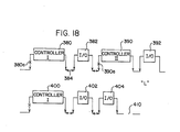
- This general concept is illustrated schematically in FIGURE 18.
- Separate controller 380 is a separate card or board having a left set of terminals isolated by separation at position 380a.
- the second board 382 is an 1/0 board controlled by processor 380.
- a motherboard 384 connects the control module 380 with the I/O module 382.
- controller 390 can be on a card inserted into the next module receptacle. By providing an isolation of the pins or terminals on the left side of extension 70 for the board supporting controller 390, controller 390 is isolated from controller 380.
- systems using bus network L can be isolated providing electrical discontinuity of the terminals on either edge of extension 70.
- the same concept is employed in the lower portion of FIGURE 18 for controller 400 used with output modules 402, 404. At the right end of this system, there is an opening 410 which isolates the system from any subsequent system connected to bus network L.
- the upper continuous conductor bus network S may not be employed in frame or rack A.
- a modified frame Al as schematically illustrated in FIGURE 19, could be used.
- This frame has a motherboard recess 500 extending along area D.
- Recess 500 supports a motherboard unit 502 which is snapped in place and held therby a series of detents 504.
- Motherboard unit 502 has spaced module receptacles 510-522 for receiving board edge extensions 60 as previously described.
Landscapes
- Engineering & Computer Science (AREA)
- Theoretical Computer Science (AREA)
- Microelectronics & Electronic Packaging (AREA)
- General Engineering & Computer Science (AREA)
- Physics & Mathematics (AREA)
- General Physics & Mathematics (AREA)
- Computer Hardware Design (AREA)
- Small-Scale Networks (AREA)
- Multi Processors (AREA)
- Communication Control (AREA)
- Structure Of Telephone Exchanges (AREA)
Applications Claiming Priority (2)
| Application Number | Priority Date | Filing Date | Title |
|---|---|---|---|
| US464342 | 1983-02-07 | ||
| US06/464,342 US4647123A (en) | 1983-02-07 | 1983-02-07 | Bus networks for digital data processing systems and modules usable therewith |
Publications (2)
| Publication Number | Publication Date |
|---|---|
| EP0117954A2 true EP0117954A2 (de) | 1984-09-12 |
| EP0117954A3 EP0117954A3 (de) | 1986-03-19 |
Family
ID=23843545
Family Applications (1)
| Application Number | Title | Priority Date | Filing Date |
|---|---|---|---|
| EP83307854A Withdrawn EP0117954A3 (de) | 1983-02-07 | 1983-12-22 | Busnetze für digitale Datenverarbeitungssysteme und brauchbares Modul dafür |
Country Status (4)
| Country | Link |
|---|---|
| US (1) | US4647123A (de) |
| EP (1) | EP0117954A3 (de) |
| JP (1) | JPS59146323A (de) |
| CA (1) | CA1231166A (de) |
Cited By (12)
| Publication number | Priority date | Publication date | Assignee | Title |
|---|---|---|---|---|
| GB2173349A (en) * | 1985-03-29 | 1986-10-08 | Gec Avionics | Electric circuit module arrangements |
| DE3510820A1 (de) * | 1985-03-26 | 1986-10-09 | Erhardt & Leimer GmbH, 8900 Augsburg | Vorrichtung zur elektronischen steuerung und regelung von maschinen |
| FR2611394A1 (fr) * | 1987-02-26 | 1988-09-02 | Ibm | Montage d'une carte d'adaptation dans un micro-ordinateur a profil bas |
| EP0226765A3 (en) * | 1985-11-08 | 1989-03-22 | American Telephone And Telegraph Company | Variable length backplane bus |
| EP0302351A3 (en) * | 1987-08-03 | 1990-07-25 | Siemens Aktiengesellschaft | Electronical apparatus |
| EP0410861A1 (de) * | 1989-07-27 | 1991-01-30 | Bull S.A. | Aufbau eines zwei Bus enthaltenden Rechnersystems |
| WO1991004539A1 (en) * | 1989-09-25 | 1991-04-04 | Cabletron Systems, Inc. | Flexible module interconnect system |
| EP0315792A3 (de) * | 1987-11-06 | 1991-12-18 | Loral Aerospace Corporation | Zwischenschaltungssystem für integrierte Halbleiterschaltungen |
| EP0491480A3 (en) * | 1990-12-17 | 1992-09-23 | Hewlett-Packard Company | Computer addressing method and apparatus |
| EP0668566A1 (de) * | 1994-02-16 | 1995-08-23 | International Business Machines Corporation | PCMCIA/- und VMC-Buskartenschnittstellenanpassungseinrichtung |
| US5740379A (en) * | 1994-08-19 | 1998-04-14 | Siemens Aktiengesellschaft | Method for generating unique addresses for electrical devices from input bit patterns being verifiable for admissibility |
| EP0840541A1 (de) * | 1996-11-05 | 1998-05-06 | Tulip Computers International B.V. | Videokarte |
Families Citing this family (49)
| Publication number | Priority date | Publication date | Assignee | Title |
|---|---|---|---|---|
| USD306429S (en) | 1986-10-30 | 1990-03-06 | American Telephone And Telegraph Company | Circuit module mounting apparatus |
| JPS63184815A (ja) * | 1987-01-27 | 1988-07-30 | Matsushita Electric Ind Co Ltd | デ−タ処理装置 |
| US4853831A (en) * | 1987-02-12 | 1989-08-01 | Nec Corporation | Bus connection structure for interruption control system |
| JPH01112681A (ja) * | 1987-07-31 | 1989-05-01 | Toshiba Corp | ハイブリッド化プリント基板 |
| EP0372021A4 (en) * | 1988-02-05 | 1993-07-28 | Commodore-Amiga, Inc. | Universal connector device |
| US4954949A (en) * | 1988-02-05 | 1990-09-04 | Commodore-Amiga, Inc. | Universal connector device for bus networks in host computer/co-processor computer system |
| US5006961A (en) * | 1988-04-25 | 1991-04-09 | Catene Systems Corporation | Segmented backplane for multiple microprocessing modules |
| US5162675A (en) * | 1989-04-14 | 1992-11-10 | Digital Communications Associates, Inc. | Dual personal computer architecture peripheral adapter board and circuit |
| CA2067599A1 (en) * | 1991-06-10 | 1992-12-11 | Bruce Alan Smith | Personal computer with riser connector for alternate master |
| US5440755A (en) * | 1992-04-06 | 1995-08-08 | Accelerated Systems, Inc. | Computer system with a processor-direct universal bus connector and interchangeable bus translator |
| US5402078A (en) * | 1992-10-13 | 1995-03-28 | Micro Control Company | Interconnection system for burn-in boards |
| US5536176A (en) * | 1994-05-25 | 1996-07-16 | Tandem Computers Incorporated | Flexible bus routing structure |
| US5572688A (en) * | 1994-09-30 | 1996-11-05 | Tyan Computer Corporation | Primary bus processing element with multifunction interconnection to secondary bus |
| US5719860A (en) * | 1996-03-22 | 1998-02-17 | Tellabs Wireless, Inc. | Wideband bus for wireless base station |
| KR100472173B1 (ko) * | 1997-05-07 | 2005-07-07 | 삼성전자주식회사 | 확장에지를갖는카드 |
| KR100241596B1 (ko) * | 1997-11-24 | 2000-02-01 | 윤종용 | 온 보드된 스카시를 이용하여 레이드 기능을 구현하는 컴퓨터시스템 |
| US6025990A (en) * | 1997-12-30 | 2000-02-15 | Intel Corporation | Processor support assembly |
| US6111757A (en) * | 1998-01-16 | 2000-08-29 | International Business Machines Corp. | SIMM/DIMM memory module |
| JP3263362B2 (ja) * | 1998-06-05 | 2002-03-04 | 三菱電機株式会社 | データ処理装置 |
| KR100355223B1 (ko) * | 1999-01-07 | 2002-10-09 | 삼성전자 주식회사 | 멀티 인라인 메모리 모듈 및 그와 결합되는 전자 부품 소켓 |
| JP2000277944A (ja) * | 1999-03-24 | 2000-10-06 | Ando Electric Co Ltd | 増設用の基板および基板の増設方法 |
| CA2302925C (en) | 1999-06-07 | 2009-05-19 | Ekstrom Industries, Inc. | Watthour meter socket adapter with circuit board mounts |
| JP3621608B2 (ja) * | 1999-07-28 | 2005-02-16 | ケル株式会社 | マザーボード |
| US6362974B1 (en) * | 2000-03-20 | 2002-03-26 | Hewlett-Packard Company | Stacked processor construction and a method for producing same |
| US6454585B1 (en) | 2001-08-01 | 2002-09-24 | Compaq Information Technologies Group, L.P. | Low profile NIC jumper solution using ZIF connector |
| US6903939B1 (en) * | 2002-04-19 | 2005-06-07 | Turnstone Systems, Inc. | Physical architecture for design of high density metallic cross connect systems |
| US6811414B1 (en) * | 2003-05-16 | 2004-11-02 | Tyco Electronics Corporation | Electrical connector module with multiple card edge sections |
| US7535718B2 (en) * | 2003-08-20 | 2009-05-19 | Imation Corp. | Memory card compatible with multiple connector standards |
| US7721118B1 (en) | 2004-09-27 | 2010-05-18 | Nvidia Corporation | Optimizing power and performance for multi-processor graphics processing |
| US8066515B2 (en) * | 2004-11-17 | 2011-11-29 | Nvidia Corporation | Multiple graphics adapter connection systems |
| US8134568B1 (en) | 2004-12-15 | 2012-03-13 | Nvidia Corporation | Frame buffer region redirection for multiple graphics adapters |
| US8212831B1 (en) | 2004-12-15 | 2012-07-03 | Nvidia Corporation | Broadcast aperture remapping for multiple graphics adapters |
| US7172465B2 (en) * | 2005-02-22 | 2007-02-06 | Micron Technology, Inc. | Edge connector including internal layer contact, printed circuit board and electronic module incorporating same |
| US8239594B2 (en) * | 2005-11-10 | 2012-08-07 | Datacard Corporation | Modular card issuance system and method of operation |
| TW200734887A (en) * | 2006-03-08 | 2007-09-16 | Tyan Computer Corp | Computing system and I/O board thereof |
| US7481659B2 (en) * | 2007-01-05 | 2009-01-27 | Imation Corp. | Multiconnector memory card |
| US7792914B2 (en) * | 2008-01-14 | 2010-09-07 | Aten International Co., Ltd. | Server with network-based remote access and server management functions using reduced number of network connections |
| TWI354213B (en) * | 2008-04-01 | 2011-12-11 | Inventec Corp | Server |
| KR20100030126A (ko) | 2008-09-09 | 2010-03-18 | 삼성전자주식회사 | 메모리 장치 및 그를 포함하는 전자 장치 |
| CN102693666A (zh) * | 2011-04-22 | 2012-09-26 | 张朋月 | 一种万用实验底板装置 |
| TW201314445A (zh) * | 2011-09-16 | 2013-04-01 | Hon Hai Prec Ind Co Ltd | 固態硬碟及安裝有該固態硬碟的電腦系統 |
| TWI553443B (zh) * | 2011-11-17 | 2016-10-11 | 華碩電腦股份有限公司 | 擴充卡 |
| USD729250S1 (en) * | 2013-07-30 | 2015-05-12 | Samsung Electronics Co., Ltd. | Semiconductor memory device |
| JP6754031B2 (ja) * | 2015-12-25 | 2020-09-09 | 北川工業株式会社 | クリップ及び固定機構 |
| JP6981859B2 (ja) * | 2017-11-28 | 2021-12-17 | タイコエレクトロニクスジャパン合同会社 | コネクタ |
| US11895797B2 (en) * | 2018-08-27 | 2024-02-06 | Sew-Eurodrive Gmbh & Co. Kg | Electrical device including a connection part and a cover part connected to the connection part |
| US11585835B2 (en) * | 2021-01-15 | 2023-02-21 | Red Lion Controls, Inc. | System of determining the sequence and positioning of pluggable modules |
| CN114256660A (zh) * | 2021-12-14 | 2022-03-29 | 东莞立讯技术有限公司 | 电连接器 |
| JP2023139826A (ja) * | 2022-03-22 | 2023-10-04 | キオクシア株式会社 | 基板及びメモリシステム |
Family Cites Families (13)
| Publication number | Priority date | Publication date | Assignee | Title |
|---|---|---|---|---|
| US3368117A (en) * | 1966-06-13 | 1968-02-06 | Ncr Co | Voltage distribution circuit arrangements for high-density packaging of electronic systems |
| US3815099A (en) * | 1970-04-01 | 1974-06-04 | Digital Equipment Corp | Data processing system |
| US3710324A (en) * | 1970-04-01 | 1973-01-09 | Digital Equipment Corp | Data processing system |
| US3675083A (en) * | 1970-09-14 | 1972-07-04 | Digital Equipment Corp | Universal bus arrangement for data processing systems |
| US3699396A (en) * | 1971-04-21 | 1972-10-17 | Honeywell Bull Soc Ind | Mounting system for printed circuit boards |
| US3867000A (en) * | 1973-09-10 | 1975-02-18 | Gte Automatic Electric Lab Inc | Latching spring clip device for securing electrical cable connectors to printed wiring cards |
| US3993935A (en) * | 1974-12-16 | 1976-11-23 | Xerox Corporation | Printed circuit board connection |
| US4050098A (en) * | 1975-11-17 | 1977-09-20 | Gulf & Western Industries, Inc. | Self-addressing modules for programmable controller |
| US4016369A (en) * | 1976-03-09 | 1977-04-05 | Bell Telephone Laboratories, Incorporated | Addressing arrangements for communications networks |
| JPS5597625A (en) * | 1979-01-17 | 1980-07-25 | Fanuc Ltd | Bus connection system |
| US4253087A (en) * | 1979-03-08 | 1981-02-24 | Nestar Systems Incorporated | Self-assigning address system |
| US4241381A (en) * | 1979-04-04 | 1980-12-23 | Amp Incorporated | Bus bar assembly for circuit cards |
| SE423777B (sv) * | 1980-09-29 | 1982-05-24 | Asea Ab | Elektrisk utrustning innefattande ett antal samarbetande kretskort |
-
1983
- 1983-02-07 US US06/464,342 patent/US4647123A/en not_active Expired - Fee Related
- 1983-12-22 EP EP83307854A patent/EP0117954A3/de not_active Withdrawn
-
1984
- 1984-01-18 CA CA000445494A patent/CA1231166A/en not_active Expired
- 1984-02-07 JP JP59020685A patent/JPS59146323A/ja active Pending
Cited By (24)
| Publication number | Priority date | Publication date | Assignee | Title |
|---|---|---|---|---|
| DE3510820A1 (de) * | 1985-03-26 | 1986-10-09 | Erhardt & Leimer GmbH, 8900 Augsburg | Vorrichtung zur elektronischen steuerung und regelung von maschinen |
| EP0196032A3 (de) * | 1985-03-26 | 1989-04-19 | Erhardt & Leimer GmbH | Vorrichtung zur elektronischen Steuerung und Regelung von Maschinen |
| GB2173349A (en) * | 1985-03-29 | 1986-10-08 | Gec Avionics | Electric circuit module arrangements |
| EP0226765A3 (en) * | 1985-11-08 | 1989-03-22 | American Telephone And Telegraph Company | Variable length backplane bus |
| FR2611394A1 (fr) * | 1987-02-26 | 1988-09-02 | Ibm | Montage d'une carte d'adaptation dans un micro-ordinateur a profil bas |
| EP0279906A3 (en) * | 1987-02-26 | 1988-12-28 | International Business Machines Corporation | Adapter card mounting in a low profile microcomputer |
| BE1000953A3 (fr) * | 1987-02-26 | 1989-05-23 | Ibm | Montage d'une carte d'adaptation dans un micro-ordinateur a profil bas. |
| EP0302351A3 (en) * | 1987-08-03 | 1990-07-25 | Siemens Aktiengesellschaft | Electronical apparatus |
| EP0315792A3 (de) * | 1987-11-06 | 1991-12-18 | Loral Aerospace Corporation | Zwischenschaltungssystem für integrierte Halbleiterschaltungen |
| EP0410861A1 (de) * | 1989-07-27 | 1991-01-30 | Bull S.A. | Aufbau eines zwei Bus enthaltenden Rechnersystems |
| FR2650414A1 (fr) * | 1989-07-27 | 1991-02-01 | Bull Sa | Architecture de systeme informatique comportant deux bus |
| US5225967A (en) * | 1989-07-27 | 1993-07-06 | Bull, S.A. | Information processing system architecture including two buses |
| US5115235A (en) * | 1989-09-25 | 1992-05-19 | Cabletron Systems, Inc. | Flexible module interconnect system |
| WO1991004539A1 (en) * | 1989-09-25 | 1991-04-04 | Cabletron Systems, Inc. | Flexible module interconnect system |
| US5349343A (en) * | 1989-09-25 | 1994-09-20 | Cabletron Systems, Inc. | Flexible module interconnect system |
| EP0491480A3 (en) * | 1990-12-17 | 1992-09-23 | Hewlett-Packard Company | Computer addressing method and apparatus |
| US5437019A (en) * | 1990-12-17 | 1995-07-25 | Hewlett-Packard Company | Addressing method and apparatus for a computer system |
| EP0668566A1 (de) * | 1994-02-16 | 1995-08-23 | International Business Machines Corporation | PCMCIA/- und VMC-Buskartenschnittstellenanpassungseinrichtung |
| GB2287106A (en) * | 1994-02-16 | 1995-09-06 | Ibm | Connection of adaptors for multiple bus architectures |
| US5761447A (en) * | 1994-02-16 | 1998-06-02 | International Business Machines Corp. | Adaptor connection apparatus for simultaneously connecting a plurality of adaptors to diverse bus architectures |
| US5740379A (en) * | 1994-08-19 | 1998-04-14 | Siemens Aktiengesellschaft | Method for generating unique addresses for electrical devices from input bit patterns being verifiable for admissibility |
| EP0840541A1 (de) * | 1996-11-05 | 1998-05-06 | Tulip Computers International B.V. | Videokarte |
| NL1004429C2 (nl) * | 1996-11-05 | 1998-05-08 | Tulip Computers International | Videokaart. |
| US6126452A (en) * | 1996-11-05 | 2000-10-03 | Tulips Computers International B.V. | Video card |
Also Published As
| Publication number | Publication date |
|---|---|
| EP0117954A3 (de) | 1986-03-19 |
| CA1231166A (en) | 1988-01-05 |
| JPS59146323A (ja) | 1984-08-22 |
| US4647123A (en) | 1987-03-03 |
Similar Documents
| Publication | Publication Date | Title |
|---|---|---|
| US4647123A (en) | Bus networks for digital data processing systems and modules usable therewith | |
| US6081048A (en) | Modular peripheral unit expandable by modules and having an automatically establishing electrical connection | |
| US3675083A (en) | Universal bus arrangement for data processing systems | |
| JP2543312B2 (ja) | コンピュ―タ・アセンブリ | |
| US5523747A (en) | Asset management in a cable management system | |
| US5432505A (en) | Cable management system with automatic mapping | |
| GB2148056A (en) | Expandable modular sequence control system | |
| JPS6011828B2 (ja) | モジユ−ル型ハ−ドウエアのパツケ−ジ装置 | |
| CN102891391A (zh) | 双堆叠紧凑型闪存卡连接器 | |
| US5547386A (en) | Apparatus adapted for coaction with a number of circuit boards | |
| US5785533A (en) | Termination panel for control unit | |
| HK160395A (en) | Assembly support for electronic or electromechanical plug-in-panel assemblies | |
| DE68928725T2 (de) | Anschlusspunkt und Schnittstellenvorrichtung | |
| KR100351188B1 (ko) | 모듈카드 | |
| JP3660552B2 (ja) | 相互接続システム | |
| US20020127895A1 (en) | Electrical apparatus including a bus conductor section | |
| JP2002026235A (ja) | メモリモジュール及びメモリモジュールソケット並びにこれらを含むシステムボード | |
| US4674007A (en) | Method and apparatus for facilitating production of electronic circuit boards | |
| US6382983B2 (en) | Module mounting system | |
| US6519145B1 (en) | ETSI/NEBS housing structure | |
| US6174196B1 (en) | Low-cost multi-shelf cabling arrangement | |
| JPH05225129A (ja) | 装着可能な構造グループ支持体用のバスシステム | |
| US4226492A (en) | Electrical interconnection apparatus | |
| US5989061A (en) | Low profile backplane jumper board | |
| US5951334A (en) | Junction box for printed circuits |
Legal Events
| Date | Code | Title | Description |
|---|---|---|---|
| PUAI | Public reference made under article 153(3) epc to a published international application that has entered the european phase |
Free format text: ORIGINAL CODE: 0009012 |
|
| AK | Designated contracting states |
Designated state(s): AT BE CH DE FR GB IT LI LU NL SE |
|
| 17P | Request for examination filed |
Effective date: 19841128 |
|
| PUAL | Search report despatched |
Free format text: ORIGINAL CODE: 0009013 |
|
| AK | Designated contracting states |
Kind code of ref document: A3 Designated state(s): AT BE CH DE FR GB IT LI LU NL SE |
|
| RAP1 | Party data changed (applicant data changed or rights of an application transferred) |
Owner name: EAGLE SIGNAL CONTROLS CORP. |
|
| 17Q | First examination report despatched |
Effective date: 19880325 |
|
| STAA | Information on the status of an ep patent application or granted ep patent |
Free format text: STATUS: THE APPLICATION IS DEEMED TO BE WITHDRAWN |
|
| 18D | Application deemed to be withdrawn |
Effective date: 19880805 |
|
| PGFP | Annual fee paid to national office [announced via postgrant information from national office to epo] |
Ref country code: GB Payment date: 19890131 Year of fee payment: 6 |
|
| RIN1 | Information on inventor provided before grant (corrected) |
Inventor name: BAKER, DENNIS G. Inventor name: MAY, WILLIAM L. Inventor name: MILLER, DAVID D. Inventor name: CHIN, DANIEL Y.S. |