EP0115792A2 - Bloc d'alimentation pour un appareil avec opération en attente, en particulier un téléviseur - Google Patents
Bloc d'alimentation pour un appareil avec opération en attente, en particulier un téléviseur Download PDFInfo
- Publication number
- EP0115792A2 EP0115792A2 EP84100344A EP84100344A EP0115792A2 EP 0115792 A2 EP0115792 A2 EP 0115792A2 EP 84100344 A EP84100344 A EP 84100344A EP 84100344 A EP84100344 A EP 84100344A EP 0115792 A2 EP0115792 A2 EP 0115792A2
- Authority
- EP
- European Patent Office
- Prior art keywords
- power supply
- voltage
- supply according
- primary side
- secondary side
- Prior art date
- Legal status (The legal status is an assumption and is not a legal conclusion. Google has not performed a legal analysis and makes no representation as to the accuracy of the status listed.)
- Granted
Links
Images

Classifications
-
- H—ELECTRICITY
- H04—ELECTRIC COMMUNICATION TECHNIQUE
- H04N—PICTORIAL COMMUNICATION, e.g. TELEVISION
- H04N5/00—Details of television systems
- H04N5/63—Generation or supply of power specially adapted for television receivers
-
- H—ELECTRICITY
- H02—GENERATION; CONVERSION OR DISTRIBUTION OF ELECTRIC POWER
- H02M—APPARATUS FOR CONVERSION BETWEEN AC AND AC, BETWEEN AC AND DC, OR BETWEEN DC AND DC, AND FOR USE WITH MAINS OR SIMILAR POWER SUPPLY SYSTEMS; CONVERSION OF DC OR AC INPUT POWER INTO SURGE OUTPUT POWER; CONTROL OR REGULATION THEREOF
- H02M3/00—Conversion of dc power input into dc power output
- H02M3/22—Conversion of dc power input into dc power output with intermediate conversion into ac
- H02M3/24—Conversion of dc power input into dc power output with intermediate conversion into ac by static converters
- H02M3/28—Conversion of dc power input into dc power output with intermediate conversion into ac by static converters using discharge tubes with control electrode or semiconductor devices with control electrode to produce the intermediate ac
- H02M3/325—Conversion of dc power input into dc power output with intermediate conversion into ac by static converters using discharge tubes with control electrode or semiconductor devices with control electrode to produce the intermediate ac using devices of a triode or a transistor type requiring continuous application of a control signal
- H02M3/335—Conversion of dc power input into dc power output with intermediate conversion into ac by static converters using discharge tubes with control electrode or semiconductor devices with control electrode to produce the intermediate ac using devices of a triode or a transistor type requiring continuous application of a control signal using semiconductor devices only
- H02M3/33569—Conversion of dc power input into dc power output with intermediate conversion into ac by static converters using discharge tubes with control electrode or semiconductor devices with control electrode to produce the intermediate ac using devices of a triode or a transistor type requiring continuous application of a control signal using semiconductor devices only having several active switching elements
Definitions
- a switched-mode power supply enables the desired galvanic separation of the receiver circuit from the mains, is much smaller and lighter than a mains transformer due to its high operating frequency in the order of 30 kHz and can generate a large number of operating voltages of different sizes and polarities on its primary side by means of appropriate windings or taps.
- the essential operating voltages must be switched off or reduced to a much smaller value, while at least one operating voltage must remain for the remote control receiver and possibly a tuner.
- the invention has for its object to provide a switching power supply that has a particularly low power consumption in standby mode with a simple structure.
- a particularly low power consumption of the order of 5 W is achieved with little switching effort in standby mode. This is particularly important for energy reasons, because the device only works in standby mode for the majority of the time of approx. 90% the power consumed in standby mode is practically lost.
- Normal operation is only initiated by a targeted intervention from the secondary side to the primary side via a route that is ineffective in standby mode. This switchover to normal operation can be carried out deliberately soft by means of a corresponding low pass in the way of the manipulated variable, so that the transition from standby to normal operation takes place without dangerous voltage jumps or peak currents.
- Another advantage is that the path that triggers normal operation from the secondary side to the primary side in standby mode, that is to say the majority of the time, is completely ineffective, that is to say without current, and therefore likewise does not consume any power.
- the components in this way are not subject to wear during standby operation. If an error, such as an interruption, occurs in the above-mentioned way, the switched-mode power supply inevitably goes into the non-hazardous standby mode, so that undefined conditions and damage cannot occur.
- a DC voltage obtained on the primary side in known circuits anyway by rectifying the pulse voltage can advantageously be used, so that the circuit complexity remains low.
- a control voltage derived from an operating voltage is also transmitted in order to stabilize the operating voltages.
- This control voltage is preferably derived directly from an operating voltage, the stabilization of which is particularly important. In a television receiver, this is primarily the main operating voltage of the order of 150 V, which also supplies the line output stage. There this operating voltage is evaluated for the control itself and the control is not carried out in a known manner only on the primary side, this operating voltage is stabilized particularly well. This also results in low crosstalk between the individual operating voltages. This is particularly important for crosstalk between the operating voltage for the sound output stage and the operating voltage for the line output stage. As is known, the sound output stage has a strongly fluctuating power consumption depending on the volume set, which means that the size of the operating voltage for the line output stage can change in an undesirable manner and can cause disturbances in the reproduced image.
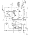
- the switched-mode power supply according to FIG. 1 contains on the primary side of the isolating transformer 1 the mains rectifier 2, the charging capacitor 3, the current measuring resistor 4, the working winding 5, the switching transistor 6, the feedback winding 7 used to generate vibrations and the thyristor used to periodically switch off the transistor 6 8.
- the secondary winding 14 supplies an operating voltage U1 of 150 V via the rectifier 15 at the terminal f.
- a tap of the winding 14 supplies the operating voltage U2 for the remote control receiver 18 via the rectifier 16 and the zener diode 17 used for voltage stabilization at the terminal g.
- Another secondary winding 19 supplies the rectifier ter 20 at terminal i a further operating voltage U3.
- the dash-dotted line 34 indicates the galvanic separation point between the network and the receiver circuit.
- the first, low voltage value for standby mode and the second, larger voltage value for normal mode apply at terminals f and i.
- the various operating modes and additional modules are described below.
- the remote control receiver 18 which is constantly supplied with operating voltage U2, supplies the manipulated variable 22 with a positive value.
- the transistor 35 is conductive and shorts the point a to earth. There is therefore no voltage at point a and the transistor 36 has no current.
- the light-emitting diode 43 of the oppocoupler 23 likewise receives no voltage, and no light reaches the phototransistor 33, so that the latter is also blocked.
- the collector-emitter path of transistor 33 lies between points b, c. At point b is a direct voltage obtained from the winding 7 with the rectifier 37 from the pulse voltage.
- the point c is the ignition electrode of the thyristor 8.
- the blocked transistor 33 has no influence on the two points b and c.
- the current flowing through the transistor 6 is switched off each time the thyristor 8 is ignited. This ignition takes place when a voltage of +0.8 V occurs at the ignition electrode, ie at point c compared to point d. The voltage effective there depends on the current through the resistor 4. By changing the voltage at point c, the switch-off time of the transistor 6 and thus the amplitude of the pulse voltage and thus also the generated operating voltages can be changed.
- the circuit described is dimensioned as follows. The ignition of the thyristor 8 and the switching off of the transistor 6 take place early, ie at such a low value of the current il through the work winding 5 that only the power required for standby operation of about 5 W is transmitted to the secondary side of the isolating transformer 1.
- the voltages U1 and U3 then have their low values of 15 V or 1.2 V, at which the connected stages are ineffective in the desired manner, that is to say the receiver is practically switched off. This voltage reduction would also decrease the voltage at points h and g, so that the remote control receiver 18 would also no longer work.
- the circuit with transistors 25, 26, 27 is provided, which acts as an electronic switch between points f and h. The transistor 25 is blocked by grounding the point a, so that the transistors 26, 27 are conductive.
- the conductive collector-emitter path of the transistor 27 connects the points f and h, so that the operating voltage U1 with its low value of 15 V is now desirably available at point h as a voltage for generating the voltage U2 for the remote control receiver 18 is.
- This circuit is described in more detail in the earlier patent application P 32 23 756.
- the receiver 18 When switching from standby to normal operation, the receiver 18 receives a signal from a remote control unit and then generates the manipulated variable 22 with the voltage value zero.
- the transistor 35 is blocked. This causes the voltage from point h to reach point a via resistor 39, so that voltage 40 at point a slowly increases due to the action of capacitor 41.
- the light-emitting diode of the Otto coupler 23 is now supplied with an initially large current, so that the transistor 33 becomes conductive.
- point b is connected to point c, that is, the ignition electrode of thyristor 8. This will get the negative voltage from point b to the ignition electrode of the thyristor 8, so that it is biased in the negative direction.
- the thyristor 8 Since the thyristor 8 only ignites at a voltage of +0.7 V at point c compared to point d, a much larger voltage must now drop for the ignition via the resistor 4. Since this voltage is proportional to the current il, the current il now reaches such a high value that the power of approximately 100 W required for normal operation is transmitted to the secondary side.
- the voltages U1 and U3 assume their high values of 150 V and 12 V, respectively.
- the transistor 25 becomes conductive, blocks the transistors 26, 27 and separates the points f, h of different voltages from one another again.
- a control voltage Ur derived from Ul via the voltage divider 42 reaches the base of the transistor 36 and reduces the current through the light-emitting diode of the optocoupler to a value which is necessary for maintaining the voltage Ul is.
- the optocoupler 23 thus transmits a quasi-digital manipulated variable supplied from point a to switch the primary side to that for normal be necessary conditions and also from point f the control voltage Ur for the continuous stabilization of the amplitude of the generated operating voltages.
- the Zener diode 44 serves as a voltage reference element for evaluating the control voltage Ur for controlling the transistor 36.
- the thyristor 28 is additionally connected to the secondary winding 19, to the control electrode of which point h is connected via the voltage divider 29,30.
- the thyristor 28 remains blocked by appropriate measurement of the resistors 29,30 and has practically the Circuit no influence.
- the thyristor 28 ignites and forms a heavy load on the transformer for the current-carrying phase. As a result, the feedback voltage at the feedback winding 7 breaks down, so that the switching power supply no longer oscillates. This circuit is described in more detail in the earlier application P 32 20 188.
- the capacitor 41 in FIG. 1 brings about the desired slow increase in the manipulated variable 40.
- the manipulated variable which initiates normal operation only appears briefly when it is generated, for example, by a so-called wiping contact of the mains switch of the device.
- the manipulated variable must be transmitted without delay via the optocoupler 23 so that the switching power supply can switch over to normal operation for the short duration of the manipulated variable.
- the capacitor 45 is provided in parallel to the zener diode 44 in FIG. 1, while the capacitor 41 is not applicable.
- the capacitor 45 forms a short circuit for a brief, pulse-like manipulated variable, so that a sufficiently high current can immediately flow through the photodiode 43, which causes the switchover to normal operation on the primary side in the manner described.
- the resistor 38 ensures that the capacitor 45 is discharged again and again at the time of switch-on, even when it is switched on briefly.
- the capacitor 45 has no effect.
- the abrupt increase in manipulated variable 40 described is shown in dashed lines.
- Pulse behavior of the primary side during normal operation and standby operation Figure 2 shows the current il through the working winding 5 and the voltage U CE across the collector-emitter path of the transistor 6 for normal operation and a power transmission of 100 W.
- the working frequency is 36 kHz.
- Figure 3 shows the values of Figure 2 for standby mode.
- the current i1 reaches correspondingly lower values because the current flow duration of the transistor 6 is controlled by the thyristor 8 to a lower value.
- the operating frequency is approximately half the value in normal operation, that is approximately 18 kHz, and is advantageously outside the hearing range. This reduced frequency is advantageous because when the frequency rises, as in known circuits, the switching transistor 6 no longer works properly as a switch because of the then low current amplitude, and the power loss on this transistor is increased.
- the power consumption in standby mode according to FIG. 3 is approximately 5 W.
- the optocoupler 23 In standby mode, the optocoupler 23 is blocked, see above that the control voltage Ur serving to stabilize the operating voltages is not effective. Nevertheless, the effective voltage U2 for the remote control receiver 18 changes only slightly, even when the mains voltage changes significantly. This is explained on the basis of FIG. 4.
- the current i1 rises to a value of 0.5 A and is then switched off with the transistor 6.
- periodic switch-on takes place again with a period of T1.
- Current i1 is switched off when point c is positive by +0.7 V compared to point d.
- the rise in the current il At a mains voltage of 110 V, the rise in the current il is correspondingly flatter because of the reduced voltage at the charging capacitor 3.
- the switch-off takes place again at the same voltage value at the resistor 4 and thus at the same value of the current il, but later because of the flatter rise.
- This reduced frequency of the pulses occurring at the transformer 5 reduces the transmitted energy, so that the value of the voltage U2 also drops.
- the relative change from T1 to T2 is significantly less than the relative change in the mains voltage of 50%. Therefore, the voltage U2 changes only slightly when there is a major change in the mains voltage.
- a slight change in the voltage U2 for the remote control receiver 18 is also uncritical because its power consumption is small and therefore a stabilization of the operating voltage is possible with simple means, for example a Zener diode.
Landscapes
- Engineering & Computer Science (AREA)
- Power Engineering (AREA)
- Multimedia (AREA)
- Signal Processing (AREA)
- Television Receiver Circuits (AREA)
- Dc-Dc Converters (AREA)
- Rectifiers (AREA)
- Details Of Television Scanning (AREA)
- Two-Way Televisions, Distribution Of Moving Picture Or The Like (AREA)
- Control Of Electrical Variables (AREA)
- Direct Current Feeding And Distribution (AREA)
- Input Circuits Of Receivers And Coupling Of Receivers And Audio Equipment (AREA)
- Details Of Television Systems (AREA)
Priority Applications (1)
| Application Number | Priority Date | Filing Date | Title |
|---|---|---|---|
| AT84100344T ATE34256T1 (de) | 1983-01-31 | 1984-01-14 | Schaltnetzteil fuer ein geraet mit bereitschaftsbetrieb, insbesondere einen fernsehempfaenger. |
Applications Claiming Priority (2)
| Application Number | Priority Date | Filing Date | Title |
|---|---|---|---|
| DE3303114 | 1983-01-31 | ||
| DE3303114A DE3303114C2 (de) | 1983-01-31 | 1983-01-31 | Selbstschwingendes Schaltnetzteil für ein Gerät mit Bereitschaftsbetrieb, insbesondere einen Fernsehempfänger |
Publications (3)
| Publication Number | Publication Date |
|---|---|
| EP0115792A2 true EP0115792A2 (fr) | 1984-08-15 |
| EP0115792A3 EP0115792A3 (en) | 1985-12-11 |
| EP0115792B1 EP0115792B1 (fr) | 1988-05-11 |
Family
ID=6189629
Family Applications (1)
| Application Number | Title | Priority Date | Filing Date |
|---|---|---|---|
| EP84100344A Expired EP0115792B1 (fr) | 1983-01-31 | 1984-01-14 | Bloc d'alimentation pour un appareil avec opération en attente, en particulier un téléviseur |
Country Status (6)
| Country | Link |
|---|---|
| EP (1) | EP0115792B1 (fr) |
| JP (1) | JPH0815325B2 (fr) |
| KR (1) | KR920002050B1 (fr) |
| AT (1) | ATE34256T1 (fr) |
| DE (2) | DE3303114C2 (fr) |
| ES (1) | ES529285A0 (fr) |
Cited By (2)
| Publication number | Priority date | Publication date | Assignee | Title |
|---|---|---|---|---|
| EP0214680B1 (fr) * | 1985-08-26 | 1990-10-31 | Koninklijke Philips Electronics N.V. | Circuit d'alimentation à commutation à deux états |
| GB2365268A (en) * | 2000-07-28 | 2002-02-13 | Motorola Israel Ltd | Antenna switch that reduces interference caused during linearisation by preventing training signals being transmitted or leaked |
Families Citing this family (2)
| Publication number | Priority date | Publication date | Assignee | Title |
|---|---|---|---|---|
| DE3341074A1 (de) * | 1983-11-12 | 1985-05-23 | Telefunken Fernseh Und Rundfunk Gmbh, 3000 Hannover | Schaltnetzteil, insbesondere fuer einen fernsehempfaenger, mit einer schutzschaltung zur begrenzung des primaerstroms |
| DE4321948C3 (de) * | 1993-07-01 | 1999-02-25 | Siemens Ag | Standby-Schaltung für elektrische Verbraucher |
Citations (2)
| Publication number | Priority date | Publication date | Assignee | Title |
|---|---|---|---|---|
| DE2620191A1 (de) | 1976-05-07 | 1977-11-17 | Graetz Gmbh & Co Ohg | Schaltnetzteil fuer die versorgung eines fernsehgeraetes |
| DE2919905A1 (de) | 1979-05-17 | 1980-11-20 | Standard Elektrik Lorenz Ag | Schaltnetzteil nach dem sperrwandleroder flusswandlerprinzip |
Family Cites Families (2)
| Publication number | Priority date | Publication date | Assignee | Title |
|---|---|---|---|---|
| DE2651196C2 (de) * | 1976-11-10 | 1986-06-26 | Telefunken Fernseh Und Rundfunk Gmbh, 3000 Hannover | Schaltnetzteil für ein Gerät der Nachrichtentechnik, insbesondere einen Fernsehempfänger |
| DE3223756C2 (de) * | 1982-06-25 | 1984-08-23 | Licentia Patent-Verwaltungs-Gmbh, 6000 Frankfurt | Schaltnetzteil für ein elektrisches Gerät mit Bereitschaftsbetrieb, insbesondere einen Fernsehempfänger |
-
1983
- 1983-01-31 DE DE3303114A patent/DE3303114C2/de not_active Expired
-
1984
- 1984-01-14 DE DE8484100344T patent/DE3471212D1/de not_active Expired
- 1984-01-14 EP EP84100344A patent/EP0115792B1/fr not_active Expired
- 1984-01-14 AT AT84100344T patent/ATE34256T1/de not_active IP Right Cessation
- 1984-01-30 ES ES529285A patent/ES529285A0/es active Granted
- 1984-01-31 KR KR1019840000428A patent/KR920002050B1/ko not_active IP Right Cessation
- 1984-01-31 JP JP59014570A patent/JPH0815325B2/ja not_active Expired - Lifetime
Patent Citations (2)
| Publication number | Priority date | Publication date | Assignee | Title |
|---|---|---|---|---|
| DE2620191A1 (de) | 1976-05-07 | 1977-11-17 | Graetz Gmbh & Co Ohg | Schaltnetzteil fuer die versorgung eines fernsehgeraetes |
| DE2919905A1 (de) | 1979-05-17 | 1980-11-20 | Standard Elektrik Lorenz Ag | Schaltnetzteil nach dem sperrwandleroder flusswandlerprinzip |
Cited By (3)
| Publication number | Priority date | Publication date | Assignee | Title |
|---|---|---|---|---|
| EP0214680B1 (fr) * | 1985-08-26 | 1990-10-31 | Koninklijke Philips Electronics N.V. | Circuit d'alimentation à commutation à deux états |
| GB2365268A (en) * | 2000-07-28 | 2002-02-13 | Motorola Israel Ltd | Antenna switch that reduces interference caused during linearisation by preventing training signals being transmitted or leaked |
| GB2365268B (en) * | 2000-07-28 | 2002-10-09 | Motorola Israel Ltd | Antenna switch |
Also Published As
| Publication number | Publication date |
|---|---|
| DE3471212D1 (en) | 1988-06-16 |
| EP0115792B1 (fr) | 1988-05-11 |
| JPS59143476A (ja) | 1984-08-17 |
| EP0115792A3 (en) | 1985-12-11 |
| ES8503898A1 (es) | 1985-04-01 |
| KR840007493A (ko) | 1984-12-07 |
| ATE34256T1 (de) | 1988-05-15 |
| KR920002050B1 (ko) | 1992-03-10 |
| DE3303114A1 (de) | 1984-08-09 |
| DE3303114C2 (de) | 1985-08-29 |
| ES529285A0 (es) | 1985-04-01 |
| JPH0815325B2 (ja) | 1996-02-14 |
Similar Documents
| Publication | Publication Date | Title |
|---|---|---|
| EP0309892B1 (fr) | Alimentation de puissance à découpage | |
| EP0143359A1 (fr) | Alimentation à découpage plus particulièrement pour récepteur de télévision avec circuit de protection pour limiter le courant primaire | |
| EP0097884B1 (fr) | Bloc d'alimentation de commande, pour un dispositif avec fonctionnement de réserve, particulièrement un récepteur de télévision | |
| DE19652604A1 (de) | Netzteil für ein Gerät mit Standby-Betrieb | |
| DE2607463C2 (de) | Schaltungsanordnung zum Schutz eines Schwingkreises gegen Überlast | |
| DE3645149C2 (fr) | ||
| DE3303114C2 (de) | Selbstschwingendes Schaltnetzteil für ein Gerät mit Bereitschaftsbetrieb, insbesondere einen Fernsehempfänger | |
| EP0299405B1 (fr) | Alimentation à découpage | |
| DE19529333B4 (de) | Selbsterregender Rücklaufkonverter und Verfahren zur Steuerung eines selbsterregenden Rücklaufkonverters | |
| DE19830758B4 (de) | Schaltnetzteil | |
| DE2910593C2 (de) | Schaltnetzteil, insbesondere für einen Fernsehempfänger | |
| EP0197045B1 (fr) | Arrangement d'un circuit pour l'alimentation d'un recepteur de television | |
| DE2804694A1 (de) | Getaktetes netzgeraet | |
| DE19613453C2 (de) | Schaltungsanordnung für ein Schaltnetzteil | |
| EP0096300B1 (fr) | Dispositif d'alimentation à découpage, plus particulièrement pour récepteur de télévision | |
| DE2755607C2 (fr) | ||
| DE3444035C2 (fr) | ||
| DE3518676A1 (de) | Schaltnetzteil fuer ein geraet mit bereitschaftsbetrieb, insbesondere einen fernsehempfaenger | |
| DE3705249C2 (fr) | ||
| EP0131703B1 (fr) | Dispositif d'alimentation à découpage pour un dispositif à fonctionnement de disponibilité, spécialement pour un récepteur de télévision | |
| EP0228582B1 (fr) | Circuit pour la génération d'une tension de fonctionnement et d'un courant de déflection horizontal | |
| EP0701318A1 (fr) | Alimentation à découpage | |
| DE3319785C2 (de) | Schaltnetzteil für ein elektrisches Gerät mit Bereitschaftsbetrieb, insbesondere einem Fernsehempfänger | |
| DE4245072B4 (de) | Freischwingendes Schaltnetzteil | |
| DD205310A1 (de) | Schutzschaltungsanordnung zum selbsttaetigen abschalten bei ueberstrom in schaltnetzteilen |
Legal Events
| Date | Code | Title | Description |
|---|---|---|---|
| PUAI | Public reference made under article 153(3) epc to a published international application that has entered the european phase |
Free format text: ORIGINAL CODE: 0009012 |
|
| AK | Designated contracting states |
Designated state(s): AT BE CH DE FR GB IT LI LU NL SE |
|
| PUAL | Search report despatched |
Free format text: ORIGINAL CODE: 0009013 |
|
| AK | Designated contracting states |
Designated state(s): AT BE CH DE FR GB IT LI LU NL SE |
|
| 17P | Request for examination filed |
Effective date: 19860211 |
|
| 17Q | First examination report despatched |
Effective date: 19870119 |
|
| ITF | It: translation for a ep patent filed |
Owner name: BARZANO' E ZANARDO MILANO S.P.A. |
|
| GRAA | (expected) grant |
Free format text: ORIGINAL CODE: 0009210 |
|
| AK | Designated contracting states |
Kind code of ref document: B1 Designated state(s): AT BE CH DE FR GB IT LI LU NL SE |
|
| REF | Corresponds to: |
Ref document number: 34256 Country of ref document: AT Date of ref document: 19880515 Kind code of ref document: T |
|
| GBT | Gb: translation of ep patent filed (gb section 77(6)(a)/1977) | ||
| REF | Corresponds to: |
Ref document number: 3471212 Country of ref document: DE Date of ref document: 19880616 |
|
| ET | Fr: translation filed | ||
| PLBI | Opposition filed |
Free format text: ORIGINAL CODE: 0009260 |
|
| 26 | Opposition filed |
Opponent name: BLAUPUNKT-WERKE GMBH Effective date: 19890210 |
|
| NLR1 | Nl: opposition has been filed with the epo |
Opponent name: BLAUPUKT-WERKE GMBH |
|
| ITTA | It: last paid annual fee | ||
| PLBN | Opposition rejected |
Free format text: ORIGINAL CODE: 0009273 |
|
| STAA | Information on the status of an ep patent application or granted ep patent |
Free format text: STATUS: OPPOSITION REJECTED |
|
| 27O | Opposition rejected |
Effective date: 19910402 |
|
| NLR2 | Nl: decision of opposition | ||
| EPTA | Lu: last paid annual fee | ||
| EAL | Se: european patent in force in sweden |
Ref document number: 84100344.5 |
|
| REG | Reference to a national code |
Ref country code: CH Ref legal event code: PFA Free format text: THOMSON CONSUMER ELECTRONIC SALES GMBH |
|
| NLT1 | Nl: modifications of names registered in virtue of documents presented to the patent office pursuant to art. 16 a, paragraph 1 |
Owner name: THOMSON CONSUMER ELECTRONICS SALES GMBH TE HANNOVE |
|
| PGFP | Annual fee paid to national office [announced via postgrant information from national office to epo] |
Ref country code: LU Payment date: 19960101 Year of fee payment: 13 |
|
| PGFP | Annual fee paid to national office [announced via postgrant information from national office to epo] |
Ref country code: SE Payment date: 19960126 Year of fee payment: 13 Ref country code: BE Payment date: 19960126 Year of fee payment: 13 Ref country code: AT Payment date: 19960126 Year of fee payment: 13 |
|
| PGFP | Annual fee paid to national office [announced via postgrant information from national office to epo] |
Ref country code: NL Payment date: 19960129 Year of fee payment: 13 |
|
| PGFP | Annual fee paid to national office [announced via postgrant information from national office to epo] |
Ref country code: CH Payment date: 19960206 Year of fee payment: 13 |
|
| PG25 | Lapsed in a contracting state [announced via postgrant information from national office to epo] |
Ref country code: LU Free format text: LAPSE BECAUSE OF NON-PAYMENT OF DUE FEES Effective date: 19970114 Ref country code: AT Effective date: 19970114 |
|
| PG25 | Lapsed in a contracting state [announced via postgrant information from national office to epo] |
Ref country code: SE Effective date: 19970115 |
|
| PG25 | Lapsed in a contracting state [announced via postgrant information from national office to epo] |
Ref country code: LI Effective date: 19970131 Ref country code: CH Effective date: 19970131 Ref country code: BE Effective date: 19970131 |
|
| BERE | Be: lapsed |
Owner name: THOMSON CONSUMER ELECTRONICS SALES G.M.B.H. Effective date: 19970131 |
|
| PG25 | Lapsed in a contracting state [announced via postgrant information from national office to epo] |
Ref country code: NL Effective date: 19970801 |
|
| REG | Reference to a national code |
Ref country code: GB Ref legal event code: 746 Effective date: 19970808 |
|
| REG | Reference to a national code |
Ref country code: CH Ref legal event code: PL |
|
| NLV4 | Nl: lapsed or anulled due to non-payment of the annual fee |
Effective date: 19970801 |
|
| EUG | Se: european patent has lapsed |
Ref document number: 84100344.5 |
|
| REG | Reference to a national code |
Ref country code: GB Ref legal event code: IF02 |
|
| PGFP | Annual fee paid to national office [announced via postgrant information from national office to epo] |
Ref country code: GB Payment date: 20021205 Year of fee payment: 20 |
|
| PGFP | Annual fee paid to national office [announced via postgrant information from national office to epo] |
Ref country code: FR Payment date: 20030113 Year of fee payment: 20 |
|
| PGFP | Annual fee paid to national office [announced via postgrant information from national office to epo] |
Ref country code: DE Payment date: 20030204 Year of fee payment: 20 |
|
| PG25 | Lapsed in a contracting state [announced via postgrant information from national office to epo] |
Ref country code: GB Free format text: LAPSE BECAUSE OF EXPIRATION OF PROTECTION Effective date: 20040113 |
|
| REG | Reference to a national code |
Ref country code: GB Ref legal event code: PE20 |
|
| APAH | Appeal reference modified |
Free format text: ORIGINAL CODE: EPIDOSCREFNO |