EP0113161A2 - Procédé pour la fabrication d'un transistor à effet de champ à grille Schottky - Google Patents
Procédé pour la fabrication d'un transistor à effet de champ à grille Schottky Download PDFInfo
- Publication number
- EP0113161A2 EP0113161A2 EP83304872A EP83304872A EP0113161A2 EP 0113161 A2 EP0113161 A2 EP 0113161A2 EP 83304872 A EP83304872 A EP 83304872A EP 83304872 A EP83304872 A EP 83304872A EP 0113161 A2 EP0113161 A2 EP 0113161A2
- Authority
- EP
- European Patent Office
- Prior art keywords
- layer
- insulation layer
- semiconductor body
- electrode
- portions
- Prior art date
- Legal status (The legal status is an assumption and is not a legal conclusion. Google has not performed a legal analysis and makes no representation as to the accuracy of the status listed.)
- Granted
Links
- 230000005669 field effect Effects 0.000 title claims description 10
- 238000004519 manufacturing process Methods 0.000 title claims description 6
- 238000009413 insulation Methods 0.000 claims abstract description 40
- 239000004065 semiconductor Substances 0.000 claims abstract description 30
- 125000006850 spacer group Chemical group 0.000 claims abstract description 20
- 239000007769 metal material Substances 0.000 claims abstract description 14
- 239000000758 substrate Substances 0.000 claims abstract description 9
- 230000004888 barrier function Effects 0.000 claims abstract description 5
- 238000000034 method Methods 0.000 claims description 37
- 229920002120 photoresistant polymer Polymers 0.000 claims description 18
- BASFCYQUMIYNBI-UHFFFAOYSA-N platinum Chemical compound [Pt] BASFCYQUMIYNBI-UHFFFAOYSA-N 0.000 claims description 12
- JBRZTFJDHDCESZ-UHFFFAOYSA-N AsGa Chemical compound [As]#[Ga] JBRZTFJDHDCESZ-UHFFFAOYSA-N 0.000 claims description 11
- 229910001218 Gallium arsenide Inorganic materials 0.000 claims description 10
- 238000005530 etching Methods 0.000 claims description 10
- 229910052782 aluminium Inorganic materials 0.000 claims description 8
- 239000004411 aluminium Substances 0.000 claims description 8
- 229910052697 platinum Inorganic materials 0.000 claims description 6
- XAGFODPZIPBFFR-UHFFFAOYSA-N aluminium Chemical compound [Al] XAGFODPZIPBFFR-UHFFFAOYSA-N 0.000 claims description 5
- 150000001875 compounds Chemical class 0.000 claims description 4
- 238000000151 deposition Methods 0.000 claims description 4
- 229910000927 Ge alloy Inorganic materials 0.000 claims description 2
- 229910052581 Si3N4 Inorganic materials 0.000 claims description 2
- BYDQGSVXQDOSJJ-UHFFFAOYSA-N [Ge].[Au] Chemical compound [Ge].[Au] BYDQGSVXQDOSJJ-UHFFFAOYSA-N 0.000 claims description 2
- 238000005229 chemical vapour deposition Methods 0.000 claims description 2
- 239000011810 insulating material Substances 0.000 claims description 2
- 238000001020 plasma etching Methods 0.000 claims description 2
- HQVNEWCFYHHQES-UHFFFAOYSA-N silicon nitride Chemical compound N12[Si]34N5[Si]62N3[Si]51N64 HQVNEWCFYHHQES-UHFFFAOYSA-N 0.000 claims description 2
- 239000000463 material Substances 0.000 claims 6
- 229910052751 metal Inorganic materials 0.000 description 11
- 239000002184 metal Substances 0.000 description 11
- 230000003071 parasitic effect Effects 0.000 description 5
- 229910017401 Au—Ge Inorganic materials 0.000 description 3
- HEMHJVSKTPXQMS-UHFFFAOYSA-M Sodium hydroxide Chemical compound [OH-].[Na+] HEMHJVSKTPXQMS-UHFFFAOYSA-M 0.000 description 3
- 229910045601 alloy Inorganic materials 0.000 description 3
- 239000000956 alloy Substances 0.000 description 3
- 238000005268 plasma chemical vapour deposition Methods 0.000 description 3
- VYZAMTAEIAYCRO-UHFFFAOYSA-N Chromium Chemical compound [Cr] VYZAMTAEIAYCRO-UHFFFAOYSA-N 0.000 description 1
- GPXJNWSHGFTCBW-UHFFFAOYSA-N Indium phosphide Chemical compound [In]#P GPXJNWSHGFTCBW-UHFFFAOYSA-N 0.000 description 1
- VYPSYNLAJGMNEJ-UHFFFAOYSA-N Silicium dioxide Chemical compound O=[Si]=O VYPSYNLAJGMNEJ-UHFFFAOYSA-N 0.000 description 1
- 238000005275 alloying Methods 0.000 description 1
- 239000007864 aqueous solution Substances 0.000 description 1
- 230000015572 biosynthetic process Effects 0.000 description 1
- 229910052804 chromium Inorganic materials 0.000 description 1
- 239000011651 chromium Substances 0.000 description 1
- 238000007796 conventional method Methods 0.000 description 1
- 230000007423 decrease Effects 0.000 description 1
- 239000012535 impurity Substances 0.000 description 1
- 238000005468 ion implantation Methods 0.000 description 1
- 238000005259 measurement Methods 0.000 description 1
- 238000001259 photo etching Methods 0.000 description 1
- 238000000206 photolithography Methods 0.000 description 1
- 230000000717 retained effect Effects 0.000 description 1
- 230000000630 rising effect Effects 0.000 description 1
- 238000004904 shortening Methods 0.000 description 1
- 229910052710 silicon Inorganic materials 0.000 description 1
- 239000010703 silicon Substances 0.000 description 1
- 229910052814 silicon oxide Inorganic materials 0.000 description 1
Images


Classifications
-
- H—ELECTRICITY
- H01—ELECTRIC ELEMENTS
- H01L—SEMICONDUCTOR DEVICES NOT COVERED BY CLASS H10
- H01L29/00—Semiconductor devices adapted for rectifying, amplifying, oscillating or switching, or capacitors or resistors with at least one potential-jump barrier or surface barrier, e.g. PN junction depletion layer or carrier concentration layer; Details of semiconductor bodies or of electrodes thereof ; Multistep manufacturing processes therefor
- H01L29/66—Types of semiconductor device ; Multistep manufacturing processes therefor
- H01L29/66007—Multistep manufacturing processes
- H01L29/66075—Multistep manufacturing processes of devices having semiconductor bodies comprising group 14 or group 13/15 materials
- H01L29/66227—Multistep manufacturing processes of devices having semiconductor bodies comprising group 14 or group 13/15 materials the devices being controllable only by the electric current supplied or the electric potential applied, to an electrode which does not carry the current to be rectified, amplified or switched, e.g. three-terminal devices
- H01L29/66409—Unipolar field-effect transistors
- H01L29/66848—Unipolar field-effect transistors with a Schottky gate, i.e. MESFET
- H01L29/66856—Unipolar field-effect transistors with a Schottky gate, i.e. MESFET with an active layer made of a group 13/15 material
- H01L29/66863—Lateral single gate transistors
-
- H—ELECTRICITY
- H01—ELECTRIC ELEMENTS
- H01L—SEMICONDUCTOR DEVICES NOT COVERED BY CLASS H10
- H01L29/00—Semiconductor devices adapted for rectifying, amplifying, oscillating or switching, or capacitors or resistors with at least one potential-jump barrier or surface barrier, e.g. PN junction depletion layer or carrier concentration layer; Details of semiconductor bodies or of electrodes thereof ; Multistep manufacturing processes therefor
- H01L29/66—Types of semiconductor device ; Multistep manufacturing processes therefor
- H01L29/68—Types of semiconductor device ; Multistep manufacturing processes therefor controllable by only the electric current supplied, or only the electric potential applied, to an electrode which does not carry the current to be rectified, amplified or switched
- H01L29/76—Unipolar devices, e.g. field effect transistors
- H01L29/772—Field effect transistors
- H01L29/80—Field effect transistors with field effect produced by a PN or other rectifying junction gate, i.e. potential-jump barrier
- H01L29/812—Field effect transistors with field effect produced by a PN or other rectifying junction gate, i.e. potential-jump barrier with a Schottky gate
Definitions
- This invention relates to a method of fabricating a Schottky gate field effect transistor (FET), and more particularly, to a method of fabricating a Schottky gate field effect transistor based on a III - V Group compound semiconductor.
- FET Schottky gate field effect transistor
- GaAs gallium arsenide
- the figure of merit of MESFETs in high frequency bands is expressed as Cgs/gm (where Cgs denotes the capacitance between the gate and source, and gm represents mutual conductance). It can be understood that the figure of merit can be improved by reducing the gate-source capacitance and/or enlarging the mutual conductance.
- the mutual conductance gm is expressed by the following formula: where:
- the mutual conductance gm is reduced to a smaller value than a maximum value gm o due to the presence of the parasitic resistance Rs.
- Rs parasitic resistance
- the enlargement of the mutual conductance gm can also be effected by increasing gm 0 .
- the source-gate capacitance Cgs is proportional to a gate length Lg, and the intrinsic mutual conductance gm o is inversely proportional to the gate length Lg. Therefore, the shortening of the gate length Lg can reduce the source-gate capacitance Cgs and enlarge the mutual conductance gm.
- a typical process of this type is, for example, the type which utilizes the overhang of a photoresist as set forth in, for example, Electronics Letters, December 1981, pp. 944-945.
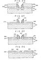
- Description will now be given with reference to Figs. lA to 1C of the fundamental steps of the process.
- a metal layer 13 used as a gate electrode is deposited on the surface of an active layer 12 formed on a GaAs substrate 11.
- a patterned photoresist 14 having a width L is formed on the metal layer 13. This metal layer 13 is selectively removed by isotropic etching with the photoresist 14 used as a mask.
- overhanging portions 14a, 14b corresponding to the extent ( ⁇ x) of the lateral etching of the metal layer 13 are formed in the photoresist 14 (Fig. 1B).
- the remaining portion 13a of the metal layer 13 is the gate electrode.
- An ohmic-contacting metal layer is deposited on the structure shown in Fig. 1B. This ohmic-contacting metal layer is divided by the photoresist 14 into two portions 15a, 15b on the active layer 12. A separate portion 15c of the ohmic-contacting metal layer is formed on the photoresist 14 (Fig. 1C).
- the photoresist 14, together with the overlying separate metal layer 15c is removed to finish the MESFET.
- the distance between the source and gate electrodes and the distance between the gate and drain electrodes are defined by a relatively small extent ( ⁇ x) of lateral etching. Therefore, the source and drain electrodes can be set close to the gate electrode, thereby reducing parasitic resistance. Further, the above-mentioned process has the advantage that the gate length can be shortened to that-which is arrived at by subtracting twice the extent ( ⁇ x) of the lateral etching from the width L of the photoresist 14.
- the aforementioned process indeed has the merit of satisfying the two previously described requirements, but this process has the drawback that difficulties are presented in rigidly controlling the extent ( ⁇ x) to which the thin metal layer used as a gate electrode is isotropically etched laterally, resulting in a decline in reproducibility.
- the conventional process presents considerable difficulties in satisfying the requirements of fixing the gate lengths over the whole surface of a wafer.
- the process of fabricating a Schottky gate FET comprises the steps of forming on a semiconductor body in a mutually facing relationship a first stack including a source electrode formed on the semiconductor body and a first spacer film formed on the planar surface of the source electrode and a second stack including a drain electrode formed on the semiconductor body and a second spacer film formed on the planar surface of the drain electrode.
- a continuous insulation layer is formed to substantially conform to the surface of the semiconductor body including the surfaces of the first and second stacks.
- the insulation layer is then anisotropically etched in the direction of its thickness, thereby allowing portions of the insulation layer to remain only on the mutually facing side walls of the first and second stacks and partially exposing the surface of the semiconductor body between the remaining portions of the insulation layer.
- the first and second spacer films are removed to expose the planar surfaces of the source and drain electrodes, thereby defining stepped portions between the remaining portions of the insulation layer and the surfaces of the respective electrodes.
- a metallic material capable of forming a Schottky barrier with the semiconductor body is deposited on the whole surface of the structure obtained by the foregoing steps, thereby forming a layer of the metallic material which is discontinuous at the stepped portions.
- the remaining portions of the insulation layer are removed to pattern the metallic material layer, thereby providing a Schottky gate electrode on that portion of the surface of the semiconductor body which is defined between the source and drain electrodes.
- a desired Schottky gate field effect transistor is fabricated.
- a distance between the source and gate electrodes, a distance between the gate and drain electrodes and a gate length are defined by the width of those portions of an insulation layer remaining on the mutually facing side walls of the first and second stacks.
- the width of the remaining portions of the insulation layer is controlled by the thickness of the insulation layer which is formed to substantially conform to the surface of the semiconductor body.
- plasma CVD plasma chemical vapor deposition
- anisotropic etching, particularly reactive ion etching can precisely control the width of those portions of the insulation layer remaining on the mutually facing side walls of the first and second stacks within an error range of 100 to 200 A or less.
- control effected by the method of this invention is far better than the conventional process of defining a distance between the source electrode and gate electrode and a distance between the drain electrode and gate electrode by means of the lateral overetching of the gate electrode, utilizing isotropic etching.
- the method of this invention very precisely controls a distance between the source electrode and gate electrode and a distance between the drain electrode and gate electrode. Therefore, the interelectrode distance is effectively reduced, enabling a MESFET having a small parasitic resistance to be fabricated with high reproducibility.
- the gate of the MESFET thus obtained has a length arrived at by subtracting a sum of the widths of both remaining portions of the insulation layer from a distance between the source and drain electrodes. Therefore, it is possible to easily realize a gate length on the order of sub- microns, which is smaller than the shortest limit attained by photolithography.
- a semiinsulating GaAs substrate 21 doped with, for example, chromium is further doped with an impurity such as silicon by, for example, ion implantation to produce an active layer 22.
- an impurity such as silicon
- a prescribed semiconductor body 20 including both the substrate 21 and the active layer 22, is provided.
- a photoresist layer 23 having a width of, for example, 1.5 pm is selectively deposited on the prescribed portion of the active layer 22, with a relatively great thickness.
- a metallic material capable of ohmic-contacting GaAs for example, a gold-germanium alloy, is deposited to a thickness of, for example, 2,000 A.
- This Au-Ge alloy is deposited in three separate portions at 24a, 24b on the surface of the active layer 22 and at 24c on the planar surface of the photoresist layer 23.
- aluminium is vapor-deposited to a thickness of, for example, 6,000 A. Namely, the aluminium is laid in three separate portions by means of the photoresist layer 23 as indicated by 25a, 25b, 25c on the surface of the corresponding Au-Ge alloy layers 24a, 24b, 24c.
- a first stack 26a comprised of the source electrode 24a and overlying aluminium spacer film 25a and a second stack comprised of the drain electrode 24b and overlying aluminium spacer film 25b are formed self-aligned.
- a distance L SD between the source electrode 24a and drain electrode 24b conforms to the width of the photoresist layer 23, i.e., 1.5 pm.
- a continuous insulation layer 27 is deposited with a thickness of, for example, 4,000 A on the whole surface of the structure shown in Fig. 2B in conformity with the physical condition of the surface.
- This conforming or conformable formation of the insulation layer 27 can be effected by the plasma CV D process or a low temperature CVD process capable of effecting excellent step coverage.
- a plasma CVD silicon nitride layer or low temperature CV D silicon oxide layer is preferred.
- the insulation layer 27 is anisotropically etched in the direction of its thickness to remove its planar portion. As shown in Fig. 2D, the separate portions 27a and 27b of the insulation layer 27 remain only on the mutually facing side walls of the first and second stacks 26a, 26b, respectively. The active layer 22 is partly exposed between the remaining portions 27a, 27b of the insulation layer 27. With the above-mentioned anisotropic etching, the width ⁇ y of the retained portions 27a, 27b of the insulation layer 27 is substantially defined by the thickness t (Fig. 2C) of the insulation layer 27, namely, is set at, for example, about 4,000 A. This condition is ascertained by a scanning type electronic microscope.
- the aluminium spacer films 25a, 25b are etched off by an aqueous solution of NaOH (Fig. 2E), for example.
- Fig. 2E aqueous solution of NaOH
- the sharply rising side walls of the remaining portions 27a, 27b of the insulation layer 27 are broadly exposed, forming stepped portions 27' between the source electrode 24a and the remaining portion 27a and also between the drain electrode 24b and the remaining portion 27b.
- the stepped portions 27' are formed on the remote sides of the remaining portions 27a, 27b.
- a metallic layer capable of constituting a Schottky barrier together with GaAs for example, a platinum layer
- a platinum layer is vapor-deposited to a thickness of, for example, 800 A on the whole surface of the structure of Fig. 2E.
- the platinum layer is made discontinuous by the aforesaid stepped portions 27' as seen from Fig. 2F. That is, the platinum layer is divided into three separate portions, namely, a portion 28a lying on the source electrode 24a, a portion 28b laid on the drain electrode 24b and a portion 28c deposited on the mutually facing sides of the remaining portions 27a, 27b of the insulation layer 27 and also on the exposed surface of the active layer 22.
- a gate electrode 28'c is formed on the active layer 22 between the source and drain electrodes.
- a desired MESFET is fabricated (Fig. 2G).
- the gate of the MESFET thus obtained has a length Lg approximately expressed as (L SD - 2 ⁇ y).
- the gate length Lg measures about 0.7 pm (1.5 pm - 0.4 pm x 2). Variations in the gate lengths of FET's produced in the same wafer were inferred from the current-voltage characteristics of the FET's. It has been ascertained that in Schottky gate field effect transistors embodying this invention, variations in the gate lengths have been reduced to about half of what was observed in the conventional type.
- the semiconductor body may be prepared not only from GaAs but also from other semiconductors including III - V Group compound semiconductors, for example, indium phosphide (InP).
- the active layer may be formed by epitaxial growth.
- the spacer film need not be exclusively formed of aluminium, but may be prepared from any other metallic material, provided it satisfies the requirement that it can be selectively etched to a greater or lesser extent than the source and drain electrodes and the conforming insulation layer (for instance, at a rate as large as 3 to 10 times or more, or as small as one-third to one-tenth or less than that at which the above-listed elements are etched).
- the stacks were formed by the lift-off method, but may be produced by the conventional photoetching process.
- the spacer film involved in the stack may be prepared from insulating material, provided it meets the above-mentioned requirement.
- the thickness of the source, gate and drain electrodes and spacer film need not be limited to the description in the foregoing embodiment. Namely, the source and drain electrodes may be formed with a thickness ranging between 2,000 A and 4,000 A, and the gate electrode may be produced with a thickness ranging from 500 A to 5,000 A.
- the spacer film may be formed with a thickness ranging between 0.5 pm and 1.5 pm.
- the conforming insulation layer may be prepared with a thickness ranging from 3,000 A to 10,000 A.
- a distance between the source and drain electrodes may be set at a level ranging between 1.5 pm and 3 pm. Obviously, the above-mentioned measurements can be suitably chosen in accordance with the desired high frequency property of the subject Schottky gate field effect transistor.
Applications Claiming Priority (2)
| Application Number | Priority Date | Filing Date | Title |
|---|---|---|---|
| JP224163/82 | 1982-12-21 | ||
| JP57224163A JPS59114871A (ja) | 1982-12-21 | 1982-12-21 | シヨツトキ−ゲ−ト型GaAs電界効果トランジスタの製造方法 |
Publications (3)
| Publication Number | Publication Date |
|---|---|
| EP0113161A2 true EP0113161A2 (fr) | 1984-07-11 |
| EP0113161A3 EP0113161A3 (en) | 1986-10-15 |
| EP0113161B1 EP0113161B1 (fr) | 1988-12-28 |
Family
ID=16809512
Family Applications (1)
| Application Number | Title | Priority Date | Filing Date |
|---|---|---|---|
| EP83304872A Expired EP0113161B1 (fr) | 1982-12-21 | 1983-08-23 | Procédé pour la fabrication d'un transistor à effet de champ à grille Schottky |
Country Status (4)
| Country | Link |
|---|---|
| US (1) | US4472872A (fr) |
| EP (1) | EP0113161B1 (fr) |
| JP (1) | JPS59114871A (fr) |
| DE (1) | DE3378806D1 (fr) |
Cited By (7)
| Publication number | Priority date | Publication date | Assignee | Title |
|---|---|---|---|---|
| EP0177129A1 (fr) * | 1984-09-29 | 1986-04-09 | Kabushiki Kaisha Toshiba | Procédé de fabrication d'un transistor à effet de champ en AsGa |
| EP0237826A2 (fr) * | 1986-03-19 | 1987-09-23 | Siemens Aktiengesellschaft | Procédé pour la fabrication d'un contact métallique auto-aligné |
| EP0287769A1 (fr) * | 1987-04-20 | 1988-10-26 | International Business Machines Corporation | MESFET rapide en GaAs ayant des contacts réfractaires et procédé de fabrication de grille à froid avec auto-alignement |
| US5024971A (en) * | 1990-08-20 | 1991-06-18 | Motorola, Inc. | Method for patterning submicron openings using an image reversal layer of material |
| EP0439114A1 (fr) * | 1990-01-24 | 1991-07-31 | Kabushiki Kaisha Toshiba | Dispositif à semiconducteurs composés possédant une électrode de grille auto-alignée par rapport aux électrodes de source et drain, et méthode de fabrication du dispositif |
| EP0484096A2 (fr) * | 1990-10-30 | 1992-05-06 | Mitsubishi Denki Kabushiki Kaisha | Procédé pour fabriquer un transistor à effet de champ ayant une porte Schottky en forme de T et encastrée |
| US9267453B2 (en) | 2013-08-22 | 2016-02-23 | Ford Global Technologies, Llc | Learning of EGR valve lift and EGR valve flow transfer function |
Families Citing this family (19)
| Publication number | Priority date | Publication date | Assignee | Title |
|---|---|---|---|---|
| JPS59229876A (ja) * | 1983-06-13 | 1984-12-24 | Toshiba Corp | シヨツトキ−ゲ−ト型電界効果トランジスタの製造方法 |
| JPS6151980A (ja) * | 1984-08-22 | 1986-03-14 | Fujitsu Ltd | 半導体装置の製造方法 |
| DE3576610D1 (de) * | 1985-12-06 | 1990-04-19 | Ibm | Verfahren zum herstellen eines voellig selbstjustierten feldeffekttransistors. |
| US4679311A (en) * | 1985-12-12 | 1987-07-14 | Allied Corporation | Method of fabricating self-aligned field-effect transistor having t-shaped gate electrode, sub-micron gate length and variable drain to gate spacing |
| JPS62199068A (ja) * | 1986-02-27 | 1987-09-02 | Toshiba Corp | 半導体装置及びその製造方法 |
| US4677736A (en) * | 1986-04-17 | 1987-07-07 | General Electric Company | Self-aligned inlay transistor with or without source and drain self-aligned metallization extensions |
| US4849717A (en) * | 1987-05-19 | 1989-07-18 | Gazelle Microcircuits, Inc. | Oscillator circuit |
| JP2612836B2 (ja) * | 1987-09-23 | 1997-05-21 | シーメンス、アクチエンゲゼルシヤフト | 自己整合ゲートを備えるmesfetの製造方法 |
| US4792531A (en) * | 1987-10-05 | 1988-12-20 | Menlo Industries, Inc. | Self-aligned gate process |
| US4947142A (en) * | 1987-12-23 | 1990-08-07 | Reza Tayrani | Attenuation controlling by means of a monolithic device |
| JP2670293B2 (ja) * | 1988-04-15 | 1997-10-29 | 富士通株式会社 | 高電子移動度トランジスタの製造方法 |
| FR2646291B1 (fr) * | 1989-04-21 | 1991-06-14 | Thomson Hybrides Microondes | Procede de realisation d'un transistor autoaligne |
| US5231040A (en) * | 1989-04-27 | 1993-07-27 | Mitsubishi Denki Kabushiki Kaisha | Method of making a field effect transistor |
| JPH04280436A (ja) * | 1990-09-28 | 1992-10-06 | Motorola Inc | 相補型自己整合hfetの製造方法 |
| US5182218A (en) * | 1991-02-25 | 1993-01-26 | Sumitomo Electric Industries, Ltd. | Production methods for compound semiconductor device having lightly doped drain structure |
| US5147812A (en) * | 1992-04-01 | 1992-09-15 | Motorola, Inc. | Fabrication method for a sub-micron geometry semiconductor device |
| US6523215B2 (en) * | 2001-04-04 | 2003-02-25 | Saint-Gobain Abrasives Technology Company | Polishing pad and system |
| DE10117741B4 (de) * | 2001-04-09 | 2008-05-21 | United Monolithic Semiconductors Gmbh | Verfahren zur Herstellung eines Halbleiter-Bauelements mit T-förmigen Kontaktelektrode |
| US6963083B2 (en) * | 2003-06-30 | 2005-11-08 | Lg.Philips Lcd Co., Ltd. | Liquid crystal display device having polycrystalline TFT and fabricating method thereof |
Citations (4)
| Publication number | Priority date | Publication date | Assignee | Title |
|---|---|---|---|---|
| DE2824026A1 (de) * | 1978-06-01 | 1979-12-20 | Licentia Gmbh | Verfahren zum herstellen eines sperrschicht-feldeffekttransistors |
| JPS57103364A (en) * | 1980-12-18 | 1982-06-26 | Nippon Telegr & Teleph Corp <Ntt> | Preparation of field-effect trasistor |
| JPS57103363A (en) * | 1980-12-18 | 1982-06-26 | Nippon Telegr & Teleph Corp <Ntt> | Manufacture of field effect transistor |
| EP0063221A2 (fr) * | 1981-04-17 | 1982-10-27 | International Business Machines Corporation | Procédé pour la fabrication d'un transistor à effet de champ |
Family Cites Families (4)
| Publication number | Priority date | Publication date | Assignee | Title |
|---|---|---|---|---|
| US4266333A (en) * | 1979-04-27 | 1981-05-12 | Rca Corporation | Method of making a Schottky barrier field effect transistor |
| US4377899A (en) * | 1979-11-19 | 1983-03-29 | Sumitomo Electric Industries, Ltd. | Method of manufacturing Schottky field-effect transistors utilizing shadow masking |
| US4359816A (en) * | 1980-07-08 | 1982-11-23 | International Business Machines Corporation | Self-aligned metal process for field effect transistor integrated circuits |
| US4426767A (en) * | 1982-01-11 | 1984-01-24 | Sperry Cororation | Selective epitaxial etch planar processing for gallium arsenide semiconductors |
-
1982
- 1982-12-21 JP JP57224163A patent/JPS59114871A/ja active Pending
-
1983
- 1983-08-16 US US06/523,600 patent/US4472872A/en not_active Expired - Lifetime
- 1983-08-23 DE DE8383304872T patent/DE3378806D1/de not_active Expired
- 1983-08-23 EP EP83304872A patent/EP0113161B1/fr not_active Expired
Patent Citations (4)
| Publication number | Priority date | Publication date | Assignee | Title |
|---|---|---|---|---|
| DE2824026A1 (de) * | 1978-06-01 | 1979-12-20 | Licentia Gmbh | Verfahren zum herstellen eines sperrschicht-feldeffekttransistors |
| JPS57103364A (en) * | 1980-12-18 | 1982-06-26 | Nippon Telegr & Teleph Corp <Ntt> | Preparation of field-effect trasistor |
| JPS57103363A (en) * | 1980-12-18 | 1982-06-26 | Nippon Telegr & Teleph Corp <Ntt> | Manufacture of field effect transistor |
| EP0063221A2 (fr) * | 1981-04-17 | 1982-10-27 | International Business Machines Corporation | Procédé pour la fabrication d'un transistor à effet de champ |
Non-Patent Citations (2)
| Title |
|---|
| PATENTS ABSTRACTS OF JAPAN, vol. 6, no. 189 (E -133)[1067], 28th September 1982; & JP - A - 57 103 363 (NIPPON DENSHIN DENWA KOSHA) 26-06-1982 * |
| PATENTS ABSTRACTS OF JAPAN, vol. 6, no. 189 (E-133)[1067], 28th September 1982; & JP - A - 57 103 364 (NIPPON DENSHIN DENWA KOSHA) 26-06-1982 * |
Cited By (15)
| Publication number | Priority date | Publication date | Assignee | Title |
|---|---|---|---|---|
| US4645563A (en) * | 1984-09-29 | 1987-02-24 | Kabushiki Kaisha Toshiba | Method of manufacturing GaAs field effect transistor |
| EP0177129A1 (fr) * | 1984-09-29 | 1986-04-09 | Kabushiki Kaisha Toshiba | Procédé de fabrication d'un transistor à effet de champ en AsGa |
| EP0237826A2 (fr) * | 1986-03-19 | 1987-09-23 | Siemens Aktiengesellschaft | Procédé pour la fabrication d'un contact métallique auto-aligné |
| DE3609274A1 (de) * | 1986-03-19 | 1987-09-24 | Siemens Ag | Verfahren zur herstellung eines selbstjustiert positionierten metallkontaktes |
| EP0237826A3 (en) * | 1986-03-19 | 1990-05-02 | Siemens Aktiengesellschaft | Method of making a self-aligned metallic contact |
| EP0287769A1 (fr) * | 1987-04-20 | 1988-10-26 | International Business Machines Corporation | MESFET rapide en GaAs ayant des contacts réfractaires et procédé de fabrication de grille à froid avec auto-alignement |
| US5409849A (en) * | 1990-01-24 | 1995-04-25 | Kabushiki Kaisha Toshiba | Method of manufacturing a compound semiconductor device having gate electrode self-aligned to source and drain electrodes |
| EP0439114A1 (fr) * | 1990-01-24 | 1991-07-31 | Kabushiki Kaisha Toshiba | Dispositif à semiconducteurs composés possédant une électrode de grille auto-alignée par rapport aux électrodes de source et drain, et méthode de fabrication du dispositif |
| US5024971A (en) * | 1990-08-20 | 1991-06-18 | Motorola, Inc. | Method for patterning submicron openings using an image reversal layer of material |
| EP0484096A3 (en) * | 1990-10-30 | 1993-05-19 | Mitsubishi Denki Kabushiki Kaisha | Method of making recessed t-shaped schottky gate field effect transistor |
| US5240869A (en) * | 1990-10-30 | 1993-08-31 | Mitsubishi Denki Kabushiki Kaisha | Method for fabricating a field effect transistor |
| EP0484096A2 (fr) * | 1990-10-30 | 1992-05-06 | Mitsubishi Denki Kabushiki Kaisha | Procédé pour fabriquer un transistor à effet de champ ayant une porte Schottky en forme de T et encastrée |
| EP0668610A2 (fr) * | 1990-10-30 | 1995-08-23 | Mitsubishi Denki Kabushiki Kaisha | Procédé de fabrication d'un transistor à effet de champ à porte Schottky |
| EP0668610A3 (fr) * | 1990-10-30 | 1995-10-11 | Mitsubishi Electric Corp | Procédé de fabrication d'un transistor à effet de champ à porte Schottky. |
| US9267453B2 (en) | 2013-08-22 | 2016-02-23 | Ford Global Technologies, Llc | Learning of EGR valve lift and EGR valve flow transfer function |
Also Published As
| Publication number | Publication date |
|---|---|
| EP0113161B1 (fr) | 1988-12-28 |
| EP0113161A3 (en) | 1986-10-15 |
| US4472872A (en) | 1984-09-25 |
| JPS59114871A (ja) | 1984-07-03 |
| DE3378806D1 (en) | 1989-02-02 |
Similar Documents
| Publication | Publication Date | Title |
|---|---|---|
| EP0113161B1 (fr) | Procédé pour la fabrication d'un transistor à effet de champ à grille Schottky | |
| US4711858A (en) | Method of fabricating a self-aligned metal-semiconductor FET having an insulator spacer | |
| US5510280A (en) | Method of making an asymmetrical MESFET having a single sidewall spacer | |
| US5384479A (en) | Field effect transistor with T-shaped gate electrode | |
| US4545109A (en) | Method of making a gallium arsenide field effect transistor | |
| EP0177129B1 (fr) | Procédé de fabrication d'un transistor à effet de champ en AsGa | |
| US4325181A (en) | Simplified fabrication method for high-performance FET | |
| US4651179A (en) | Low resistance gallium arsenide field effect transistor | |
| JPS5950567A (ja) | 電界効果トランジスタの製造方法 | |
| US4997779A (en) | Method of making asymmetrical gate field effect transistor | |
| JP3233207B2 (ja) | 電界効果トランジスタの製造方法 | |
| US5550065A (en) | Method of fabricating self-aligned FET structure having a high temperature stable T-shaped Schottky gate contact | |
| GB2230899A (en) | Method of producing a gate | |
| US5643811A (en) | Method of making field effect transistor for high-frequency operation | |
| US20080064155A1 (en) | Method for Producing a Multi-Stage Recess in a Layer Structure and a Field Effect Transistor with a Multi-Recessed Gate | |
| US5837570A (en) | Heterostructure semiconductor device and method of fabricating same | |
| US20030113985A1 (en) | Field effect transistor semiconductor and method for manufacturing the same | |
| EP0201713A1 (fr) | Procédé de fabrication de l'électrode de porte d'un TEC par évaporation oblique | |
| EP0585942A1 (fr) | MESFET à double grille | |
| JP3200917B2 (ja) | 半導体装置及びその製造方法 | |
| JPS62169483A (ja) | シヨツトキゲ−ト電界効果トランジスタの構造及び製造方法 | |
| JP2790104B2 (ja) | 電界効果トランジスタの製造方法 | |
| KR100366422B1 (ko) | 금속트랜지스터제조방법 | |
| KR100220870B1 (ko) | 화합물 반도체 장치의 제조 방법 | |
| JP2001524759A (ja) | ガリウムひ素ベースのエピタキシャル電界効果トランジスタの選択性凹部用InxGa1−xPエッチング停止層及びその製造方法 |
Legal Events
| Date | Code | Title | Description |
|---|---|---|---|
| PUAI | Public reference made under article 153(3) epc to a published international application that has entered the european phase |
Free format text: ORIGINAL CODE: 0009012 |
|
| 17P | Request for examination filed |
Effective date: 19830831 |
|
| AK | Designated contracting states |
Designated state(s): DE FR GB NL |
|
| RAP1 | Party data changed (applicant data changed or rights of an application transferred) |
Owner name: KABUSHIKI KAISHA TOSHIBA |
|
| PUAL | Search report despatched |
Free format text: ORIGINAL CODE: 0009013 |
|
| AK | Designated contracting states |
Kind code of ref document: A3 Designated state(s): DE FR GB NL |
|
| 17Q | First examination report despatched |
Effective date: 19880330 |
|
| GRAA | (expected) grant |
Free format text: ORIGINAL CODE: 0009210 |
|
| AK | Designated contracting states |
Kind code of ref document: B1 Designated state(s): DE FR GB NL |
|
| REF | Corresponds to: |
Ref document number: 3378806 Country of ref document: DE Date of ref document: 19890202 |
|
| ET | Fr: translation filed | ||
| PLBE | No opposition filed within time limit |
Free format text: ORIGINAL CODE: 0009261 |
|
| STAA | Information on the status of an ep patent application or granted ep patent |
Free format text: STATUS: NO OPPOSITION FILED WITHIN TIME LIMIT |
|
| 26N | No opposition filed | ||
| PGFP | Annual fee paid to national office [announced via postgrant information from national office to epo] |
Ref country code: FR Payment date: 19930805 Year of fee payment: 11 |
|
| PGFP | Annual fee paid to national office [announced via postgrant information from national office to epo] |
Ref country code: GB Payment date: 19930816 Year of fee payment: 11 |
|
| PGFP | Annual fee paid to national office [announced via postgrant information from national office to epo] |
Ref country code: DE Payment date: 19930823 Year of fee payment: 11 |
|
| PGFP | Annual fee paid to national office [announced via postgrant information from national office to epo] |
Ref country code: NL Payment date: 19930831 Year of fee payment: 11 |
|
| PG25 | Lapsed in a contracting state [announced via postgrant information from national office to epo] |
Ref country code: GB Effective date: 19940823 |
|
| PG25 | Lapsed in a contracting state [announced via postgrant information from national office to epo] |
Ref country code: NL Effective date: 19950301 |
|
| NLV4 | Nl: lapsed or anulled due to non-payment of the annual fee | ||
| GBPC | Gb: european patent ceased through non-payment of renewal fee |
Effective date: 19940823 |
|
| PG25 | Lapsed in a contracting state [announced via postgrant information from national office to epo] |
Ref country code: FR Effective date: 19950428 |
|
| PG25 | Lapsed in a contracting state [announced via postgrant information from national office to epo] |
Ref country code: DE Effective date: 19950503 |
|
| REG | Reference to a national code |
Ref country code: FR Ref legal event code: ST |