EP0111932B1 - Harzgekapselte Halbleiteranordnungen und ein Verfahren zum Herstellen derselben - Google Patents
Harzgekapselte Halbleiteranordnungen und ein Verfahren zum Herstellen derselben Download PDFInfo
- Publication number
- EP0111932B1 EP0111932B1 EP83112853A EP83112853A EP0111932B1 EP 0111932 B1 EP0111932 B1 EP 0111932B1 EP 83112853 A EP83112853 A EP 83112853A EP 83112853 A EP83112853 A EP 83112853A EP 0111932 B1 EP0111932 B1 EP 0111932B1
- Authority
- EP
- European Patent Office
- Prior art keywords
- epoxy resin
- sub
- assembly
- moles
- resin
- Prior art date
- Legal status (The legal status is an assumption and is not a legal conclusion. Google has not performed a legal analysis and makes no representation as to the accuracy of the status listed.)
- Expired
Links
- 239000004065 semiconductor Substances 0.000 title claims description 23
- 238000000034 method Methods 0.000 title claims description 17
- 238000004519 manufacturing process Methods 0.000 title claims description 10
- 239000003822 epoxy resin Substances 0.000 claims description 50
- 229920000647 polyepoxide Polymers 0.000 claims description 50
- 239000008188 pellet Substances 0.000 claims description 19
- 238000007789 sealing Methods 0.000 claims description 13
- 229920005989 resin Polymers 0.000 claims description 9
- 239000011347 resin Substances 0.000 claims description 9
- RAXXELZNTBOGNW-UHFFFAOYSA-N imidazole Natural products C1=CNC=N1 RAXXELZNTBOGNW-UHFFFAOYSA-N 0.000 claims description 8
- -1 imidazole compound Chemical class 0.000 claims description 6
- 239000002253 acid Substances 0.000 claims description 4
- 230000009974 thixotropic effect Effects 0.000 claims description 4
- 125000000217 alkyl group Chemical group 0.000 claims description 3
- 125000004435 hydrogen atom Chemical group [H]* 0.000 claims description 3
- 125000004029 hydroxymethyl group Chemical group [H]OC([H])([H])* 0.000 claims description 3
- 125000002496 methyl group Chemical group [H]C([H])([H])* 0.000 claims description 3
- 238000001879 gelation Methods 0.000 claims description 2
- 239000000463 material Substances 0.000 description 13
- XUIMIQQOPSSXEZ-UHFFFAOYSA-N Silicon Chemical compound [Si] XUIMIQQOPSSXEZ-UHFFFAOYSA-N 0.000 description 9
- 229910052710 silicon Inorganic materials 0.000 description 9
- 239000010703 silicon Substances 0.000 description 9
- 239000002184 metal Substances 0.000 description 8
- 229910052751 metal Inorganic materials 0.000 description 8
- 239000004593 Epoxy Substances 0.000 description 7
- 238000005219 brazing Methods 0.000 description 6
- 239000011521 glass Substances 0.000 description 4
- 239000002966 varnish Substances 0.000 description 4
- 230000007423 decrease Effects 0.000 description 3
- 238000010438 heat treatment Methods 0.000 description 3
- PXHVJJICTQNCMI-UHFFFAOYSA-N Nickel Chemical compound [Ni] PXHVJJICTQNCMI-UHFFFAOYSA-N 0.000 description 2
- 239000003795 chemical substances by application Substances 0.000 description 2
- 150000002500 ions Chemical class 0.000 description 2
- RYGMFSIKBFXOCR-UHFFFAOYSA-N Copper Chemical compound [Cu] RYGMFSIKBFXOCR-UHFFFAOYSA-N 0.000 description 1
- 241001635479 Coris bulbifrons Species 0.000 description 1
- 239000011248 coating agent Substances 0.000 description 1
- 238000000576 coating method Methods 0.000 description 1
- 229910052802 copper Inorganic materials 0.000 description 1
- 239000010949 copper Substances 0.000 description 1
- 238000010894 electron beam technology Methods 0.000 description 1
- 125000003700 epoxy group Chemical group 0.000 description 1
- LNEPOXFFQSENCJ-UHFFFAOYSA-N haloperidol Chemical compound C1CC(O)(C=2C=CC(Cl)=CC=2)CCN1CCCC(=O)C1=CC=C(F)C=C1 LNEPOXFFQSENCJ-UHFFFAOYSA-N 0.000 description 1
- 238000002844 melting Methods 0.000 description 1
- 230000008018 melting Effects 0.000 description 1
- 229910052759 nickel Inorganic materials 0.000 description 1
- 229920002050 silicone resin Polymers 0.000 description 1
- 239000002002 slurry Substances 0.000 description 1
- 238000005476 soldering Methods 0.000 description 1
- XLYOFNOQVPJJNP-UHFFFAOYSA-N water Substances O XLYOFNOQVPJJNP-UHFFFAOYSA-N 0.000 description 1
Images
Classifications
-
- H—ELECTRICITY
- H01—ELECTRIC ELEMENTS
- H01L—SEMICONDUCTOR DEVICES NOT COVERED BY CLASS H10
- H01L21/00—Processes or apparatus adapted for the manufacture or treatment of semiconductor or solid state devices or of parts thereof
- H01L21/02—Manufacture or treatment of semiconductor devices or of parts thereof
- H01L21/04—Manufacture or treatment of semiconductor devices or of parts thereof the devices having potential barriers, e.g. a PN junction, depletion layer or carrier concentration layer
- H01L21/50—Assembly of semiconductor devices using processes or apparatus not provided for in a single one of the subgroups H01L21/06 - H01L21/326, e.g. sealing of a cap to a base of a container
- H01L21/56—Encapsulations, e.g. encapsulation layers, coatings
-
- H—ELECTRICITY
- H01—ELECTRIC ELEMENTS
- H01L—SEMICONDUCTOR DEVICES NOT COVERED BY CLASS H10
- H01L23/00—Details of semiconductor or other solid state devices
- H01L23/28—Encapsulations, e.g. encapsulating layers, coatings, e.g. for protection
- H01L23/29—Encapsulations, e.g. encapsulating layers, coatings, e.g. for protection characterised by the material, e.g. carbon
- H01L23/293—Organic, e.g. plastic
-
- H—ELECTRICITY
- H01—ELECTRIC ELEMENTS
- H01L—SEMICONDUCTOR DEVICES NOT COVERED BY CLASS H10
- H01L23/00—Details of semiconductor or other solid state devices
- H01L23/28—Encapsulations, e.g. encapsulating layers, coatings, e.g. for protection
- H01L23/31—Encapsulations, e.g. encapsulating layers, coatings, e.g. for protection characterised by the arrangement or shape
- H01L23/3107—Encapsulations, e.g. encapsulating layers, coatings, e.g. for protection characterised by the arrangement or shape the device being completely enclosed
- H01L23/3135—Double encapsulation or coating and encapsulation
-
- H—ELECTRICITY
- H01—ELECTRIC ELEMENTS
- H01L—SEMICONDUCTOR DEVICES NOT COVERED BY CLASS H10
- H01L23/00—Details of semiconductor or other solid state devices
- H01L23/28—Encapsulations, e.g. encapsulating layers, coatings, e.g. for protection
- H01L23/31—Encapsulations, e.g. encapsulating layers, coatings, e.g. for protection characterised by the arrangement or shape
- H01L23/3157—Partial encapsulation or coating
- H01L23/3171—Partial encapsulation or coating the coating being directly applied to the semiconductor body, e.g. passivation layer
-
- H—ELECTRICITY
- H01—ELECTRIC ELEMENTS
- H01L—SEMICONDUCTOR DEVICES NOT COVERED BY CLASS H10
- H01L2924/00—Indexing scheme for arrangements or methods for connecting or disconnecting semiconductor or solid-state bodies as covered by H01L24/00
- H01L2924/0001—Technical content checked by a classifier
- H01L2924/0002—Not covered by any one of groups H01L24/00, H01L24/00 and H01L2224/00
-
- Y—GENERAL TAGGING OF NEW TECHNOLOGICAL DEVELOPMENTS; GENERAL TAGGING OF CROSS-SECTIONAL TECHNOLOGIES SPANNING OVER SEVERAL SECTIONS OF THE IPC; TECHNICAL SUBJECTS COVERED BY FORMER USPC CROSS-REFERENCE ART COLLECTIONS [XRACs] AND DIGESTS
- Y10—TECHNICAL SUBJECTS COVERED BY FORMER USPC
- Y10T—TECHNICAL SUBJECTS COVERED BY FORMER US CLASSIFICATION
- Y10T29/00—Metal working
- Y10T29/49—Method of mechanical manufacture
- Y10T29/49002—Electrical device making
- Y10T29/49117—Conductor or circuit manufacturing
- Y10T29/49169—Assembling electrical component directly to terminal or elongated conductor
- Y10T29/49171—Assembling electrical component directly to terminal or elongated conductor with encapsulating
Definitions
- the present invention relates to a resin-molded semiconductor device and more specifically to a resin-molded axial lead-type semiconductor device.
- the Japanese Patent Laid-Open No. 1174/1980 discloses a method according to which the sub-assembly is sealed in a glass, and the epoxy resion is further applied thereto. In this case, however, the epoxy resin which is applied forms a film which is not thick enough to achieve the purpose of sealing.
- the GB-A-1 303 382 discloses a method for manufacturing resin-molded semiconductor device comprising two steps of (1) horizontally holding the sub-assembly and coating a polyes- terimide varnish onto the semiconductor pellet while rotating the sub-assembly on the axis of the axial leads as center and (2) curing the varnish while maintaining the sub-assembly stationary without rotationg it.
- the varnish is not thick enough to achieve the purpose of sealing, because the curing of the varnish is carried out without rotating the sub-assembly.
- the object of the present invention is to provide a process for manufacturing resin-molded semi- conductor devices sealed in an epoxy resin which have high quality and reliability without employing a metal mold.
- the above problem is solved according to the claim.
- the subclaims refer to prefered embodiments.
- the present invention relates to a process which comprises the steps of:
- the heating is carried out 2 to 10 min at 160 to 180°C in step (C) and 3 to 24 h at 160 to 200° in step (D).
- the invention also relates to semiconductor devices obtained by the above-mentioned process.
- the invention can be put into practice by using an epoxy resin which has a suitable degree of hardening property and a suitable thixotropic index.
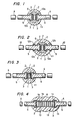
- the figs. 1 to 4 are vertical section views of resin-molded semiconductor devices according to different embodiments of the present invention.
- a silicon pellet 1 having a pn junction J has nickel-plated layers 2 on its both surfaces so that the solderiong can be easily accomplished.
- the silicon pellet 1 is held between a pair of copper header leads 4 by soldering as designated at 3.
- Silver-plated layers 5 are formed on the surfaces of the header leads 4.
- a generally used surface-stabilizing material 6 such as a silicone resin is provided around the side periphery of the silicon pellet 1, and then a sealing layer is formed by using an epoxy resin.
- a one-can epoxy resin having epoxy groups in the molecules and containing 3 to 15 moles of an organic dibasic acid dihydrazide per 100 moles of the epoxy resin, and 2 to 7 moles of an imidazole compound represented by the following formula, wherein R, is a methyl group, a hydrogen atom or a hydroxymethyl group, and R 2 is an alkyl group, per 100 moles of the epoxy resin.
- a one-can epoxy resin which does not contain an organic dibasic acid dihydrazide, but contains only the imidazole compound represented by the above formula in an amount of 2 to 20 moles per 100 moles of the epoxy resin.
- This resin exhibits a thixotropic index and hardening properties that are suited for the manufacturing process according to the invention which is described below.
- such resins exhibit a viscosity ratio of 1.0 to 2.5, as measured by a rotation viscometer under the conditions of 4 turns a minute and 20 turns a minute (thixotropic index), and exhibits a gelation time of 0.8 to 3 min in a constant temperature bath.
- the device of the embodiment of fig. 1 is manufactured as described below.
- a predetermined amount of the epoxy resin is dropped onto the sub-assembly which is provided with the surface-stabilizing material 6 and which is rotated at a speed of 2 turns a second with the leads 4 being held nearly horizontally.
- the resin will be required in an amount of about 0.05 g when it is to be applied to a length of 4 mm and to a diameter of 3.5 mm onto the sub-assembly in which the leads have a diameter of 0.6 mm and the header portions 12a have a diameter of 1.5 mm.
- the epoxy resion builds up in a shape as schematically shown in fig. 1.
- the epoxy resin in the portions where the epoxy resin comes into contact with the electrodes 4 or the surface-stabilizing material 6, it transforms into a sol due to the frictional forces produced by the rotation, whereby the viscosity decreases and the resin applies well onto the header leads 4 and the surface-stabilizing material 6.
- the frictional forces are smaller and practically only the centrifugal force is acting on these portions. Therefore, the epoxy resin is not transformed into a sol and maintains the shape as indicated in fig. 1. Then, the surface only of the epoxy resin is hardened by heating while rotating the sub-assembly. Good results will be obtained if the epoxy resin is heated 2 to 10 min at 160° to 180°C.
- the epoxy resion in the surface is once transformed into a sol by the heat and its viscosity decreases conspicuously.
- the internal epoxy resin is not transformed into a sol and has a higher viscosity than the epoxy resin in the surface. Therefore, the represented shape is roughly maintained, and the surface portion only is hardened.
- the internal epoxy resin is confined by the hardened surface portion. At this moment, therefore, the epoxy resin no more drops from the sub-assembly despite it is not rotated; i.e., the epoxy resin which is applied thereto maintains its shape. Therefore, there is no need of rotating the sub-assembly.
- the epoxy resin is heated 3 to 24 h at 160° to 200°C so that it is perfectly cured up to its internal portion, at a different place as required.
- the epoxy resin is cured by heating.
- the epoxy resin can also be cured by the generally employed methods such as irradiation with ultraviolet rays, X-rays, infrared rays, and electron beams.
- the sub-assembly can be molded without the need of using a metal mold. Therefore, the number of manufacturing steps can be reduced, and the manufacturing operation can be continuously carried out using automatic machines for the mass-production of those devices having constant quality.
- the epoxy resin is cured after it is sufficiently applied to the header leads 4 or the surface-stabilizing material 6. Therefore, the sealing layer 11 is well adhering onto the header leads 4 or the surface-stabilizing material 6. Further, since the epoxy resin does not contain a parting agent, no gap develops between the leads and the sealing layer occurring in the prior art, and there are obtained semiconductor devices having an increased moisture resistance.
- Fig. 2 illustrates another embodiment of the present invention, in which the portions same as, or corresponding to, those of fig. 1 are denoted by the same reference numerals.
- This embodiment employs double header leads 12 which have flange portions 12b at positions separated away from the header portions 12a.
- the flange portions 12b block the epoxy resin from flowing in the axial direction when it is being applied, work to trim the shape of the sealing layer 11, and contribute to a constant quality.
- Fig. 3 shows a further embodiment of the present invention, in which the portions same as, or corresponding to, those of fig. 1 are denoted by the same reference numerals.
- the above-mentioned epoxy resin does not contain movable ions such as Na + , CI- or the like, that make the exposed surfaces of pn junction J of the silicon pellet 1 unstable. Therefore, the use of the surface-stabilizing material can be eliminated so far as the epoxy resin is not contaminated by movable ions such as Na + , CI- or the like. This helps to further reduce the number of manufacturing steps.
- Fig. 4 shows still further embodiment of the present invention, in which the portions same as, or corresponding to, those of fig. 1 are denoted by the same refrence numerals.
- a plurality of silicon pellets 1a,1b,---1n having pn junctions are laminated in a predetermined rectifying direction, adhered by a brazing material 13, and are then supported between the header leads 4 by brazing with a brazing material 3.
- the brazing material 3 has a melting point lower than that of the brazing material 13, such that the laminate of silicon pellets 1a, 1 --- 1n is not deformed when it is being brazed to the header leads 4 with the brazing material 3.
- the silicon pellets 1a, 1 b, - - - 1n of fig. 4 are not provided with plated nickel layers.
- the sub-assembly can be molded sufficiently even if the distance is large between the two header leads 4.
Landscapes
- Engineering & Computer Science (AREA)
- Physics & Mathematics (AREA)
- Condensed Matter Physics & Semiconductors (AREA)
- General Physics & Mathematics (AREA)
- Computer Hardware Design (AREA)
- Microelectronics & Electronic Packaging (AREA)
- Power Engineering (AREA)
- Manufacturing & Machinery (AREA)
- Encapsulation Of And Coatings For Semiconductor Or Solid State Devices (AREA)
- Structures Or Materials For Encapsulating Or Coating Semiconductor Devices Or Solid State Devices (AREA)
- Epoxy Resins (AREA)
Claims (6)


Applications Claiming Priority (2)
| Application Number | Priority Date | Filing Date | Title |
|---|---|---|---|
| JP224483/82 | 1982-12-20 | ||
| JP57224483A JPS59113648A (ja) | 1982-12-20 | 1982-12-20 | 樹脂モ−ルド型半導体装置 |
Publications (3)
| Publication Number | Publication Date |
|---|---|
| EP0111932A2 EP0111932A2 (de) | 1984-06-27 |
| EP0111932A3 EP0111932A3 (en) | 1985-08-28 |
| EP0111932B1 true EP0111932B1 (de) | 1988-07-20 |
Family
ID=16814499
Family Applications (1)
| Application Number | Title | Priority Date | Filing Date |
|---|---|---|---|
| EP83112853A Expired EP0111932B1 (de) | 1982-12-20 | 1983-12-20 | Harzgekapselte Halbleiteranordnungen und ein Verfahren zum Herstellen derselben |
Country Status (5)
| Country | Link |
|---|---|
| US (1) | US4540603A (de) |
| EP (1) | EP0111932B1 (de) |
| JP (1) | JPS59113648A (de) |
| CA (1) | CA1206819A (de) |
| DE (1) | DE3377438D1 (de) |
Families Citing this family (11)
| Publication number | Priority date | Publication date | Assignee | Title |
|---|---|---|---|---|
| US5994041A (en) * | 1985-04-06 | 1999-11-30 | Eastman Kodak Company | Process for buffering concentrated aqueous slurries |
| JPS63283054A (ja) * | 1987-03-11 | 1988-11-18 | Fuji Plant Kogyo Kk | ピン保持部付リードフレームの製造方法 |
| US4985747A (en) * | 1988-06-09 | 1991-01-15 | Oki Electric Industry Co., Ltd. | Terminal structure and process of fabricating the same |
| US5219795A (en) * | 1989-02-07 | 1993-06-15 | Fujitsu Limited | Dual in-line packaging and method of producing the same |
| DE4110318C2 (de) * | 1991-03-28 | 2001-10-11 | Bosch Gmbh Robert | Verfahren zum Zusammenlöten zweier Bauteile |
| US5609998A (en) * | 1994-12-29 | 1997-03-11 | Eastman Kodak Company | Process for dispersing concentrated aqueous slurries |
| US5550086A (en) * | 1995-12-27 | 1996-08-27 | Tai; George | Ceramic chip form semiconductor diode fabrication method |
| US6477037B1 (en) * | 1998-04-03 | 2002-11-05 | Medtronic, Inc. | Implantable medical device having flat electrolytic capacitor with miniaturized epoxy connector droplet |
| US6008535A (en) * | 1998-09-17 | 1999-12-28 | Advanced Ceramic X Corp. | Method of making a semiconductor diode from laminated ceramic tape |
| US6700210B1 (en) | 1999-12-06 | 2004-03-02 | Micron Technology, Inc. | Electronic assemblies containing bow resistant semiconductor packages |
| US6384487B1 (en) * | 1999-12-06 | 2002-05-07 | Micron Technology, Inc. | Bow resistant plastic semiconductor package and method of fabrication |
Family Cites Families (14)
| Publication number | Priority date | Publication date | Assignee | Title |
|---|---|---|---|---|
| US3492157A (en) * | 1966-06-20 | 1970-01-27 | Tokyo Shibaura Electric Co | Resin-sealed semiconductor device and manufacturing method for the same |
| DE2027105C3 (de) * | 1970-06-03 | 1981-03-26 | Robert Bosch Gmbh, 70469 Stuttgart | Verfahren zur Herstellung eines Halbleiterbauelements |
| JPS4831965U (de) * | 1971-08-20 | 1973-04-18 | ||
| US3751724A (en) * | 1972-04-28 | 1973-08-07 | C Mcgrath | Encapsulated electrical component |
| JPS5619086B2 (de) * | 1974-03-08 | 1981-05-06 | ||
| JPS531469A (en) * | 1976-06-26 | 1978-01-09 | Hitachi Ltd | Glass seal type semiconductor device |
| JPS55111344U (de) * | 1979-01-29 | 1980-08-05 | ||
| JPS551174A (en) * | 1979-03-28 | 1980-01-07 | Hitachi Ltd | Semiconductor apparatus |
| US4282136A (en) * | 1979-04-09 | 1981-08-04 | Hunt Earl R | Flame retardant epoxy molding compound method and encapsulated device |
| JPS5629339A (en) * | 1979-08-20 | 1981-03-24 | Origin Electric Co Ltd | Glass seal of semiconductor element |
| DE2944922C2 (de) * | 1979-11-07 | 1981-11-12 | Standard Elektrik Lorenz Ag, 7000 Stuttgart | Elektrisches Bauelement |
| JPS5749126A (en) * | 1980-09-08 | 1982-03-20 | Hitachi Ltd | Bushing |
| JPS5769750A (en) * | 1980-10-17 | 1982-04-28 | Hitachi Ltd | Manufacture of semiconductor device |
| JPS57152125A (en) * | 1981-03-12 | 1982-09-20 | Nippon Electric Co | Method of sheathing electronic part |
-
1982
- 1982-12-20 JP JP57224483A patent/JPS59113648A/ja active Granted
-
1983
- 1983-12-19 US US06/563,039 patent/US4540603A/en not_active Expired - Lifetime
- 1983-12-20 DE DE8383112853T patent/DE3377438D1/de not_active Expired
- 1983-12-20 CA CA000443800A patent/CA1206819A/en not_active Expired
- 1983-12-20 EP EP83112853A patent/EP0111932B1/de not_active Expired
Also Published As
| Publication number | Publication date |
|---|---|
| JPS6347340B2 (de) | 1988-09-21 |
| EP0111932A3 (en) | 1985-08-28 |
| JPS59113648A (ja) | 1984-06-30 |
| EP0111932A2 (de) | 1984-06-27 |
| DE3377438D1 (en) | 1988-08-25 |
| CA1206819A (en) | 1986-07-02 |
| US4540603A (en) | 1985-09-10 |
Similar Documents
| Publication | Publication Date | Title |
|---|---|---|
| EP0111932B1 (de) | Harzgekapselte Halbleiteranordnungen und ein Verfahren zum Herstellen derselben | |
| US3868724A (en) | Multi-layer connecting structures for packaging semiconductor devices mounted on a flexible carrier | |
| US5057457A (en) | Multimold semiconductor device and the manufacturing method therefor | |
| EP0511162A1 (de) | Wärmeleitende Klebfilme, Laminate mit wärmeleitenden Klebschichten und deren Verwendung | |
| DE102013204344A1 (de) | Halbleitervorrichtung und Verfahren zum Herstellen selbiger | |
| JPS646538B2 (de) | ||
| US7829389B2 (en) | Roll-on encapsulation method for semiconductor packages | |
| DE2326314A1 (de) | Verfahren zur herstellung einer passivierenden schicht mit wenigstens einer kontaktoeffnung | |
| US4230754A (en) | Bonding electronic component to molded package | |
| CN1106689C (zh) | 半导体封装引线去边方法 | |
| GB2164794A (en) | Method for encapsulating semiconductor components mounted on a carrier tape | |
| US20170287729A1 (en) | Process for packaging circuit component having copper circuits with solid electrical and thermal conductivities and circuit component thereof | |
| DE102017104305A1 (de) | Halbleiterbauelement | |
| DE112016006751B4 (de) | Leistungshalbleitermodul, Leistungsumsetzungsvorrichtung, die es verwendet, und Verfahren zum Herstellen der Leistungsumsetzungsvorrichtung | |
| JPH0936177A (ja) | 半導体装置及びその製造方法 | |
| DE3019868A1 (de) | Verfahren zur herstellung von halbleiteranordnungen | |
| CN101925989B (zh) | 用于半导体封装的滚压囊封方法 | |
| US3255393A (en) | Metal to semiconductor rectifying junction | |
| US4010143A (en) | Molding compound containing N-methyl-Z pyrrolidone and method | |
| JPH0117261B2 (de) | ||
| JP2001055432A (ja) | 半導体装置封止用樹脂組成物及びこれを用いた半導体装置、並びに半導体装置製造方法及び製造装置 | |
| JPH0247106B2 (ja) | Jushimoorudogatahandotaisochi | |
| JPS62226634A (ja) | 半導体素子の製造方法 | |
| JP3309889B2 (ja) | 半導体素子の樹脂封止方法 | |
| JPS6214100B2 (de) |
Legal Events
| Date | Code | Title | Description |
|---|---|---|---|
| PUAI | Public reference made under article 153(3) epc to a published international application that has entered the european phase |
Free format text: ORIGINAL CODE: 0009012 |
|
| 17P | Request for examination filed |
Effective date: 19831229 |
|
| AK | Designated contracting states |
Designated state(s): DE FR GB |
|
| PUAL | Search report despatched |
Free format text: ORIGINAL CODE: 0009013 |
|
| AK | Designated contracting states |
Designated state(s): DE FR GB |
|
| 17Q | First examination report despatched |
Effective date: 19870511 |
|
| GRAA | (expected) grant |
Free format text: ORIGINAL CODE: 0009210 |
|
| AK | Designated contracting states |
Kind code of ref document: B1 Designated state(s): DE FR GB |
|
| REF | Corresponds to: |
Ref document number: 3377438 Country of ref document: DE Date of ref document: 19880825 |
|
| ET | Fr: translation filed | ||
| PLBE | No opposition filed within time limit |
Free format text: ORIGINAL CODE: 0009261 |
|
| STAA | Information on the status of an ep patent application or granted ep patent |
Free format text: STATUS: NO OPPOSITION FILED WITHIN TIME LIMIT |
|
| 26N | No opposition filed | ||
| REG | Reference to a national code |
Ref country code: GB Ref legal event code: IF02 |
|
| PGFP | Annual fee paid to national office [announced via postgrant information from national office to epo] |
Ref country code: FR Payment date: 20021105 Year of fee payment: 20 |
|
| PGFP | Annual fee paid to national office [announced via postgrant information from national office to epo] |
Ref country code: GB Payment date: 20021126 Year of fee payment: 20 |
|
| PGFP | Annual fee paid to national office [announced via postgrant information from national office to epo] |
Ref country code: DE Payment date: 20021205 Year of fee payment: 20 |
|
| PG25 | Lapsed in a contracting state [announced via postgrant information from national office to epo] |
Ref country code: GB Free format text: LAPSE BECAUSE OF EXPIRATION OF PROTECTION Effective date: 20031219 |
|
| REG | Reference to a national code |
Ref country code: GB Ref legal event code: PE20 |