EP0111932B1 - Resin-molded semiconductor devices and a process for manufacturing the same - Google Patents
Resin-molded semiconductor devices and a process for manufacturing the same Download PDFInfo
- Publication number
- EP0111932B1 EP0111932B1 EP83112853A EP83112853A EP0111932B1 EP 0111932 B1 EP0111932 B1 EP 0111932B1 EP 83112853 A EP83112853 A EP 83112853A EP 83112853 A EP83112853 A EP 83112853A EP 0111932 B1 EP0111932 B1 EP 0111932B1
- Authority
- EP
- European Patent Office
- Prior art keywords
- epoxy resin
- sub
- assembly
- moles
- resin
- Prior art date
- Legal status (The legal status is an assumption and is not a legal conclusion. Google has not performed a legal analysis and makes no representation as to the accuracy of the status listed.)
- Expired
Links
Images
Classifications
-
- H—ELECTRICITY
- H01—ELECTRIC ELEMENTS
- H01L—SEMICONDUCTOR DEVICES NOT COVERED BY CLASS H10
- H01L21/00—Processes or apparatus adapted for the manufacture or treatment of semiconductor or solid state devices or of parts thereof
- H01L21/02—Manufacture or treatment of semiconductor devices or of parts thereof
- H01L21/04—Manufacture or treatment of semiconductor devices or of parts thereof the devices having at least one potential-jump barrier or surface barrier, e.g. PN junction, depletion layer or carrier concentration layer
- H01L21/50—Assembly of semiconductor devices using processes or apparatus not provided for in a single one of the subgroups H01L21/06 - H01L21/326, e.g. sealing of a cap to a base of a container
- H01L21/56—Encapsulations, e.g. encapsulation layers, coatings
-
- H—ELECTRICITY
- H01—ELECTRIC ELEMENTS
- H01L—SEMICONDUCTOR DEVICES NOT COVERED BY CLASS H10
- H01L23/00—Details of semiconductor or other solid state devices
- H01L23/28—Encapsulations, e.g. encapsulating layers, coatings, e.g. for protection
- H01L23/29—Encapsulations, e.g. encapsulating layers, coatings, e.g. for protection characterised by the material, e.g. carbon
- H01L23/293—Organic, e.g. plastic
-
- H—ELECTRICITY
- H01—ELECTRIC ELEMENTS
- H01L—SEMICONDUCTOR DEVICES NOT COVERED BY CLASS H10
- H01L23/00—Details of semiconductor or other solid state devices
- H01L23/28—Encapsulations, e.g. encapsulating layers, coatings, e.g. for protection
- H01L23/31—Encapsulations, e.g. encapsulating layers, coatings, e.g. for protection characterised by the arrangement or shape
- H01L23/3107—Encapsulations, e.g. encapsulating layers, coatings, e.g. for protection characterised by the arrangement or shape the device being completely enclosed
- H01L23/3135—Double encapsulation or coating and encapsulation
-
- H—ELECTRICITY
- H01—ELECTRIC ELEMENTS
- H01L—SEMICONDUCTOR DEVICES NOT COVERED BY CLASS H10
- H01L23/00—Details of semiconductor or other solid state devices
- H01L23/28—Encapsulations, e.g. encapsulating layers, coatings, e.g. for protection
- H01L23/31—Encapsulations, e.g. encapsulating layers, coatings, e.g. for protection characterised by the arrangement or shape
- H01L23/3157—Partial encapsulation or coating
- H01L23/3171—Partial encapsulation or coating the coating being directly applied to the semiconductor body, e.g. passivation layer
-
- H—ELECTRICITY
- H01—ELECTRIC ELEMENTS
- H01L—SEMICONDUCTOR DEVICES NOT COVERED BY CLASS H10
- H01L2924/00—Indexing scheme for arrangements or methods for connecting or disconnecting semiconductor or solid-state bodies as covered by H01L24/00
- H01L2924/0001—Technical content checked by a classifier
- H01L2924/0002—Not covered by any one of groups H01L24/00, H01L24/00 and H01L2224/00
-
- Y—GENERAL TAGGING OF NEW TECHNOLOGICAL DEVELOPMENTS; GENERAL TAGGING OF CROSS-SECTIONAL TECHNOLOGIES SPANNING OVER SEVERAL SECTIONS OF THE IPC; TECHNICAL SUBJECTS COVERED BY FORMER USPC CROSS-REFERENCE ART COLLECTIONS [XRACs] AND DIGESTS
- Y10—TECHNICAL SUBJECTS COVERED BY FORMER USPC
- Y10T—TECHNICAL SUBJECTS COVERED BY FORMER US CLASSIFICATION
- Y10T29/00—Metal working
- Y10T29/49—Method of mechanical manufacture
- Y10T29/49002—Electrical device making
- Y10T29/49117—Conductor or circuit manufacturing
- Y10T29/49169—Assembling electrical component directly to terminal or elongated conductor
- Y10T29/49171—Assembling electrical component directly to terminal or elongated conductor with encapsulating
Definitions
- the present invention relates to a resin-molded semiconductor device and more specifically to a resin-molded axial lead-type semiconductor device.
- the Japanese Patent Laid-Open No. 1174/1980 discloses a method according to which the sub-assembly is sealed in a glass, and the epoxy resion is further applied thereto. In this case, however, the epoxy resin which is applied forms a film which is not thick enough to achieve the purpose of sealing.
- the GB-A-1 303 382 discloses a method for manufacturing resin-molded semiconductor device comprising two steps of (1) horizontally holding the sub-assembly and coating a polyes- terimide varnish onto the semiconductor pellet while rotating the sub-assembly on the axis of the axial leads as center and (2) curing the varnish while maintaining the sub-assembly stationary without rotationg it.
- the varnish is not thick enough to achieve the purpose of sealing, because the curing of the varnish is carried out without rotating the sub-assembly.
- the object of the present invention is to provide a process for manufacturing resin-molded semi- conductor devices sealed in an epoxy resin which have high quality and reliability without employing a metal mold.
- the above problem is solved according to the claim.
- the subclaims refer to prefered embodiments.
- the present invention relates to a process which comprises the steps of:
- the heating is carried out 2 to 10 min at 160 to 180°C in step (C) and 3 to 24 h at 160 to 200° in step (D).
- the invention also relates to semiconductor devices obtained by the above-mentioned process.
- the invention can be put into practice by using an epoxy resin which has a suitable degree of hardening property and a suitable thixotropic index.
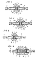
- the figs. 1 to 4 are vertical section views of resin-molded semiconductor devices according to different embodiments of the present invention.
- a silicon pellet 1 having a pn junction J has nickel-plated layers 2 on its both surfaces so that the solderiong can be easily accomplished.
- the silicon pellet 1 is held between a pair of copper header leads 4 by soldering as designated at 3.
- Silver-plated layers 5 are formed on the surfaces of the header leads 4.
- a generally used surface-stabilizing material 6 such as a silicone resin is provided around the side periphery of the silicon pellet 1, and then a sealing layer is formed by using an epoxy resin.
- a one-can epoxy resin having epoxy groups in the molecules and containing 3 to 15 moles of an organic dibasic acid dihydrazide per 100 moles of the epoxy resin, and 2 to 7 moles of an imidazole compound represented by the following formula, wherein R, is a methyl group, a hydrogen atom or a hydroxymethyl group, and R 2 is an alkyl group, per 100 moles of the epoxy resin.
- a one-can epoxy resin which does not contain an organic dibasic acid dihydrazide, but contains only the imidazole compound represented by the above formula in an amount of 2 to 20 moles per 100 moles of the epoxy resin.
- This resin exhibits a thixotropic index and hardening properties that are suited for the manufacturing process according to the invention which is described below.
- such resins exhibit a viscosity ratio of 1.0 to 2.5, as measured by a rotation viscometer under the conditions of 4 turns a minute and 20 turns a minute (thixotropic index), and exhibits a gelation time of 0.8 to 3 min in a constant temperature bath.
- the device of the embodiment of fig. 1 is manufactured as described below.
- a predetermined amount of the epoxy resin is dropped onto the sub-assembly which is provided with the surface-stabilizing material 6 and which is rotated at a speed of 2 turns a second with the leads 4 being held nearly horizontally.
- the resin will be required in an amount of about 0.05 g when it is to be applied to a length of 4 mm and to a diameter of 3.5 mm onto the sub-assembly in which the leads have a diameter of 0.6 mm and the header portions 12a have a diameter of 1.5 mm.
- the epoxy resion builds up in a shape as schematically shown in fig. 1.
- the epoxy resin in the portions where the epoxy resin comes into contact with the electrodes 4 or the surface-stabilizing material 6, it transforms into a sol due to the frictional forces produced by the rotation, whereby the viscosity decreases and the resin applies well onto the header leads 4 and the surface-stabilizing material 6.
- the frictional forces are smaller and practically only the centrifugal force is acting on these portions. Therefore, the epoxy resin is not transformed into a sol and maintains the shape as indicated in fig. 1. Then, the surface only of the epoxy resin is hardened by heating while rotating the sub-assembly. Good results will be obtained if the epoxy resin is heated 2 to 10 min at 160° to 180°C.
- the epoxy resion in the surface is once transformed into a sol by the heat and its viscosity decreases conspicuously.
- the internal epoxy resin is not transformed into a sol and has a higher viscosity than the epoxy resin in the surface. Therefore, the represented shape is roughly maintained, and the surface portion only is hardened.
- the internal epoxy resin is confined by the hardened surface portion. At this moment, therefore, the epoxy resin no more drops from the sub-assembly despite it is not rotated; i.e., the epoxy resin which is applied thereto maintains its shape. Therefore, there is no need of rotating the sub-assembly.
- the epoxy resin is heated 3 to 24 h at 160° to 200°C so that it is perfectly cured up to its internal portion, at a different place as required.
- the epoxy resin is cured by heating.
- the epoxy resin can also be cured by the generally employed methods such as irradiation with ultraviolet rays, X-rays, infrared rays, and electron beams.
- the sub-assembly can be molded without the need of using a metal mold. Therefore, the number of manufacturing steps can be reduced, and the manufacturing operation can be continuously carried out using automatic machines for the mass-production of those devices having constant quality.
- the epoxy resin is cured after it is sufficiently applied to the header leads 4 or the surface-stabilizing material 6. Therefore, the sealing layer 11 is well adhering onto the header leads 4 or the surface-stabilizing material 6. Further, since the epoxy resin does not contain a parting agent, no gap develops between the leads and the sealing layer occurring in the prior art, and there are obtained semiconductor devices having an increased moisture resistance.
- Fig. 2 illustrates another embodiment of the present invention, in which the portions same as, or corresponding to, those of fig. 1 are denoted by the same reference numerals.
- This embodiment employs double header leads 12 which have flange portions 12b at positions separated away from the header portions 12a.
- the flange portions 12b block the epoxy resin from flowing in the axial direction when it is being applied, work to trim the shape of the sealing layer 11, and contribute to a constant quality.
- Fig. 3 shows a further embodiment of the present invention, in which the portions same as, or corresponding to, those of fig. 1 are denoted by the same reference numerals.
- the above-mentioned epoxy resin does not contain movable ions such as Na + , CI- or the like, that make the exposed surfaces of pn junction J of the silicon pellet 1 unstable. Therefore, the use of the surface-stabilizing material can be eliminated so far as the epoxy resin is not contaminated by movable ions such as Na + , CI- or the like. This helps to further reduce the number of manufacturing steps.
- Fig. 4 shows still further embodiment of the present invention, in which the portions same as, or corresponding to, those of fig. 1 are denoted by the same refrence numerals.
- a plurality of silicon pellets 1a,1b,---1n having pn junctions are laminated in a predetermined rectifying direction, adhered by a brazing material 13, and are then supported between the header leads 4 by brazing with a brazing material 3.
- the brazing material 3 has a melting point lower than that of the brazing material 13, such that the laminate of silicon pellets 1a, 1 --- 1n is not deformed when it is being brazed to the header leads 4 with the brazing material 3.
- the silicon pellets 1a, 1 b, - - - 1n of fig. 4 are not provided with plated nickel layers.
- the sub-assembly can be molded sufficiently even if the distance is large between the two header leads 4.
Description
- The present invention relates to a resin-molded semiconductor device and more specifically to a resin-molded axial lead-type semiconductor device.
- Semiconductor devices have been extensively used which are obtained by sealing in an epoxy resion a sub-assembly in which a semiconductor pellet is held by between a pair of brazed axial leads. So far, however, the sub-assembly is sealed in the epoxy resion by using a metal mold. When a glass is to be used for the purpose of sealing, a slurry of glass is applied round a semiconductor pellet in the sub-assembly and is then baked. In this case, there is no need of employing a metal mold. When the epoxy resin is used, however, the metal mold must be employed unlike the case of using the glass. The reason is because there is available no one-can type epoxy resion which cures to some extent within a few minutes. Namely, such resin systems transform into a sol just before curing and the viscosity decreases strikingly relative to the viscosity at ordinary temperature. Accordingly, the resins would drop off from the sub-assembly without using a mold.
- The Japanese Patent Laid-Open No. 1174/1980 discloses a method according to which the sub-assembly is sealed in a glass, and the epoxy resion is further applied thereto. In this case, however, the epoxy resin which is applied forms a film which is not thick enough to achieve the purpose of sealing.
- According to the sealing method which is now put into practice with using epoxy resins, it is necessary to employ a metal mold. Therefore, cumbersome operation is required for setting the sub-assembly in the metal mold, injecting the epoxy resin, parting the sub-assembly from the metal mold, and the like. In particular, it is difficult to continuously perform the setting and parting, which seriously interferes with a mass-production. When a parting agent is contained in the epoxy resin to facilitate the parting operation, it reduces the adhesiveness between the resin and the leads, and gaps are often formed between the leads and the sealing layer in such semiconductor devices. Furthermore, water may infiltrate through the gaps and reach the semiconductor pellet; in such a case, the semiconductor device loses its characteristics in the reverse direction and further loses the reliability in operation.
- The GB-A-1 303 382 discloses a method for manufacturing resin-molded semiconductor device comprising two steps of (1) horizontally holding the sub-assembly and coating a polyes- terimide varnish onto the semiconductor pellet while rotating the sub-assembly on the axis of the axial leads as center and (2) curing the varnish while maintaining the sub-assembly stationary without rotationg it. In this method, the varnish is not thick enough to achieve the purpose of sealing, because the curing of the varnish is carried out without rotating the sub-assembly.
- The object of the present invention is to provide a process for manufacturing resin-molded semi- conductor devices sealed in an epoxy resin which have high quality and reliability without employing a metal mold. The above problem is solved according to the claim. The subclaims refer to prefered embodiments.
- The present invention relates to a process which comprises the steps of:
- (A) preparing a sub-assembly consisting of a semi-conductor pellet brazed between a pair of axial leads,
- (B) horizontally holding a sub-assembly and dropping a predetermined amount of an epoxy resin onto the semiconductor pellet while rotating the sub-assembly on the axis of the axial leads as center,
- (C) curing the epoxy resin while rotating the sub-assembly in such a manner that the surface portions of the epoxy resin are hardened; and
- (D) further curing the epoxy resin while maintaining the sub-assembly, stationary without rotating it and completely curing the epoxy resion, thereby forming a sealing layer of the epoxy resin around the side periphery of the semiconductor pellet.
- Preferably, the heating is carried out 2 to 10 min at 160 to 180°C in step (C) and 3 to 24 h at 160 to 200° in step (D).
- The invention also relates to semiconductor devices obtained by the above-mentioned process. The invention can be put into practice by using an epoxy resin which has a suitable degree of hardening property and a suitable thixotropic index.
- The figs. 1 to 4 are vertical section views of resin-molded semiconductor devices according to different embodiments of the present invention.
- In fig. 1, a
silicon pellet 1 having a pn junction J has nickel-platedlayers 2 on its both surfaces so that the solderiong can be easily accomplished. Thesilicon pellet 1 is held between a pair of copper header leads 4 by soldering as designated at 3. Silver-platedlayers 5 are formed on the surfaces of the header leads 4. To stabilize the surfaces of the pn junction J of thesilicon pellet 1 of the thus constructed sub-assembly, a generally used surface-stabilizingmaterial 6 such as a silicone resin is provided around the side periphery of thesilicon pellet 1, and then a sealing layer is formed by using an epoxy resin. - According to a prefered embodiment of the invention, a one-can epoxy resin is used having epoxy groups in the molecules and containing 3 to 15 moles of an organic dibasic acid dihydrazide per 100 moles of the epoxy resin, and 2 to 7 moles of an imidazole compound represented by the following formula,

- It is also preferable to use a one-can epoxy resin which does not contain an organic dibasic acid dihydrazide, but contains only the imidazole compound represented by the above formula in an amount of 2 to 20 moles per 100 moles of the epoxy resin.
- This resin exhibits a thixotropic index and hardening properties that are suited for the manufacturing process according to the invention which is described below. Preferably, such resins exhibit a viscosity ratio of 1.0 to 2.5, as measured by a rotation viscometer under the conditions of 4 turns a minute and 20 turns a minute (thixotropic index), and exhibits a gelation time of 0.8 to 3 min in a constant temperature bath.
- By using this kind of resins, the device of the embodiment of fig. 1 is manufactured as described below.
- First, a predetermined amount of the epoxy resin is dropped onto the sub-assembly which is provided with the surface-stabilizing
material 6 and which is rotated at a speed of 2 turns a second with theleads 4 being held nearly horizontally. The resin will be required in an amount of about 0.05 g when it is to be applied to a length of 4 mm and to a diameter of 3.5 mm onto the sub-assembly in which the leads have a diameter of 0.6 mm and theheader portions 12a have a diameter of 1.5 mm. As the sub-assembly rotates, the epoxy resion builds up in a shape as schematically shown in fig. 1. That is, in the portions where the epoxy resin comes into contact with theelectrodes 4 or the surface-stabilizingmaterial 6, it transforms into a sol due to the frictional forces produced by the rotation, whereby the viscosity decreases and the resin applies well onto the header leads 4 and the surface-stabilizingmaterial 6. In the portions remote from the sub-assembly, on the other hand, the frictional forces are smaller and practically only the centrifugal force is acting on these portions. Therefore, the epoxy resin is not transformed into a sol and maintains the shape as indicated in fig. 1. Then, the surface only of the epoxy resin is hardened by heating while rotating the sub-assembly. Good results will be obtained if the epoxy resin is heated 2 to 10 min at 160° to 180°C. In this case, the epoxy resion in the surface is once transformed into a sol by the heat and its viscosity decreases conspicuously. However, the internal epoxy resin is not transformed into a sol and has a higher viscosity than the epoxy resin in the surface. Therefore, the represented shape is roughly maintained, and the surface portion only is hardened. The internal epoxy resin is confined by the hardened surface portion. At this moment, therefore, the epoxy resin no more drops from the sub-assembly despite it is not rotated; i.e., the epoxy resin which is applied thereto maintains its shape. Therefore, there is no need of rotating the sub-assembly. That is, rotation of the sub-assembly is stopped, and the epoxy resin is heated 3 to 24 h at 160° to 200°C so that it is perfectly cured up to its internal portion, at a different place as required. In the above-mentioned embodiment, the epoxy resin is cured by heating. The epoxy resin, however, can also be cured by the generally employed methods such as irradiation with ultraviolet rays, X-rays, infrared rays, and electron beams. - According to this process as described above, the sub-assembly can be molded without the need of using a metal mold. Therefore, the number of manufacturing steps can be reduced, and the manufacturing operation can be continuously carried out using automatic machines for the mass-production of those devices having constant quality.
- The epoxy resin is cured after it is sufficiently applied to the header leads 4 or the surface-stabilizing
material 6. Therefore, the sealinglayer 11 is well adhering onto the header leads 4 or the surface-stabilizingmaterial 6. Further, since the epoxy resin does not contain a parting agent, no gap develops between the leads and the sealing layer occurring in the prior art, and there are obtained semiconductor devices having an increased moisture resistance. - Fig. 2 illustrates another embodiment of the present invention, in which the portions same as, or corresponding to, those of fig. 1 are denoted by the same reference numerals.
- This embodiment employs double header leads 12 which have
flange portions 12b at positions separated away from theheader portions 12a. - The
flange portions 12b block the epoxy resin from flowing in the axial direction when it is being applied, work to trim the shape of thesealing layer 11, and contribute to a constant quality. - Fig. 3 shows a further embodiment of the present invention, in which the portions same as, or corresponding to, those of fig. 1 are denoted by the same reference numerals.
- In this embodiment, no surface-stabilizing material is used, and the sub-assembly is directly wrapped in the
sealing layer 11 composed of the epoxy resin. - The above-mentioned epoxy resin does not contain movable ions such as Na+, CI- or the like, that make the exposed surfaces of pn junction J of the
silicon pellet 1 unstable. Therefore, the use of the surface-stabilizing material can be eliminated so far as the epoxy resin is not contaminated by movable ions such as Na+, CI- or the like. This helps to further reduce the number of manufacturing steps. - Fig. 4 shows still further embodiment of the present invention, in which the portions same as, or corresponding to, those of fig. 1 are denoted by the same refrence numerals.
- In this embodiment, a plurality of
silicon pellets brazing material 13, and are then supported between the header leads 4 by brazing with abrazing material 3. Thebrazing material 3 has a melting point lower than that of thebrazing material 13, such that the laminate ofsilicon pellets brazing material 3. Thesilicon pellets - There will be obtained a withstand voltage which increases in proportion to the number of
silicon pellets - According to the process of the present invention, the sub-assembly can be molded sufficiently even if the distance is large between the two header leads 4.
- According to the present invention as described above, it is possible to obtain resin-molded semi- conductor devices which can be easily sealed in a contionuous manner without using molds which are suited for being mass-produced, and which maintain high quality and reliability.
Claims (6)


Applications Claiming Priority (2)
| Application Number | Priority Date | Filing Date | Title |
|---|---|---|---|
| JP57224483A JPS59113648A (en) | 1982-12-20 | 1982-12-20 | Plastic molded type semiconductor device |
| JP224483/82 | 1982-12-20 |
Publications (3)
| Publication Number | Publication Date |
|---|---|
| EP0111932A2 EP0111932A2 (en) | 1984-06-27 |
| EP0111932A3 EP0111932A3 (en) | 1985-08-28 |
| EP0111932B1 true EP0111932B1 (en) | 1988-07-20 |
Family
ID=16814499
Family Applications (1)
| Application Number | Title | Priority Date | Filing Date |
|---|---|---|---|
| EP83112853A Expired EP0111932B1 (en) | 1982-12-20 | 1983-12-20 | Resin-molded semiconductor devices and a process for manufacturing the same |
Country Status (5)
| Country | Link |
|---|---|
| US (1) | US4540603A (en) |
| EP (1) | EP0111932B1 (en) |
| JP (1) | JPS59113648A (en) |
| CA (1) | CA1206819A (en) |
| DE (1) | DE3377438D1 (en) |
Families Citing this family (11)
| Publication number | Priority date | Publication date | Assignee | Title |
|---|---|---|---|---|
| US5994041A (en) * | 1985-04-06 | 1999-11-30 | Eastman Kodak Company | Process for buffering concentrated aqueous slurries |
| JPS63283054A (en) * | 1987-03-11 | 1988-11-18 | Fuji Plant Kogyo Kk | Lead frame with pin-holding structure and holding method for pin of lead frame |
| US4985747A (en) * | 1988-06-09 | 1991-01-15 | Oki Electric Industry Co., Ltd. | Terminal structure and process of fabricating the same |
| US5219795A (en) * | 1989-02-07 | 1993-06-15 | Fujitsu Limited | Dual in-line packaging and method of producing the same |
| DE4110318C2 (en) * | 1991-03-28 | 2001-10-11 | Bosch Gmbh Robert | Process for soldering two components together |
| US5609998A (en) * | 1994-12-29 | 1997-03-11 | Eastman Kodak Company | Process for dispersing concentrated aqueous slurries |
| US5550086A (en) * | 1995-12-27 | 1996-08-27 | Tai; George | Ceramic chip form semiconductor diode fabrication method |
| US6477037B1 (en) * | 1998-04-03 | 2002-11-05 | Medtronic, Inc. | Implantable medical device having flat electrolytic capacitor with miniaturized epoxy connector droplet |
| US6008535A (en) * | 1998-09-17 | 1999-12-28 | Advanced Ceramic X Corp. | Method of making a semiconductor diode from laminated ceramic tape |
| US6384487B1 (en) * | 1999-12-06 | 2002-05-07 | Micron Technology, Inc. | Bow resistant plastic semiconductor package and method of fabrication |
| US6700210B1 (en) * | 1999-12-06 | 2004-03-02 | Micron Technology, Inc. | Electronic assemblies containing bow resistant semiconductor packages |
Family Cites Families (14)
| Publication number | Priority date | Publication date | Assignee | Title |
|---|---|---|---|---|
| US3492157A (en) * | 1966-06-20 | 1970-01-27 | Tokyo Shibaura Electric Co | Resin-sealed semiconductor device and manufacturing method for the same |
| DE2027105C3 (en) * | 1970-06-03 | 1981-03-26 | Robert Bosch Gmbh, 70469 Stuttgart | Method for manufacturing a semiconductor component |
| JPS4831965U (en) * | 1971-08-20 | 1973-04-18 | ||
| US3751724A (en) * | 1972-04-28 | 1973-08-07 | C Mcgrath | Encapsulated electrical component |
| JPS5619086B2 (en) * | 1974-03-08 | 1981-05-06 | ||
| JPS531469A (en) * | 1976-06-26 | 1978-01-09 | Hitachi Ltd | Glass seal type semiconductor device |
| JPS55111344U (en) * | 1979-01-29 | 1980-08-05 | ||
| JPS551174A (en) * | 1979-03-28 | 1980-01-07 | Hitachi Ltd | Semiconductor apparatus |
| US4282136A (en) * | 1979-04-09 | 1981-08-04 | Hunt Earl R | Flame retardant epoxy molding compound method and encapsulated device |
| JPS5629339A (en) * | 1979-08-20 | 1981-03-24 | Origin Electric Co Ltd | Glass seal of semiconductor element |
| DE2944922C2 (en) * | 1979-11-07 | 1981-11-12 | Standard Elektrik Lorenz Ag, 7000 Stuttgart | Electrical component |
| JPS5749126A (en) * | 1980-09-08 | 1982-03-20 | Hitachi Ltd | Bushing |
| JPS5769750A (en) * | 1980-10-17 | 1982-04-28 | Hitachi Ltd | Manufacture of semiconductor device |
| JPS57152125A (en) * | 1981-03-12 | 1982-09-20 | Nippon Electric Co | Method of sheathing electronic part |
-
1982
- 1982-12-20 JP JP57224483A patent/JPS59113648A/en active Granted
-
1983
- 1983-12-19 US US06/563,039 patent/US4540603A/en not_active Expired - Lifetime
- 1983-12-20 EP EP83112853A patent/EP0111932B1/en not_active Expired
- 1983-12-20 CA CA000443800A patent/CA1206819A/en not_active Expired
- 1983-12-20 DE DE8383112853T patent/DE3377438D1/en not_active Expired
Also Published As
| Publication number | Publication date |
|---|---|
| EP0111932A2 (en) | 1984-06-27 |
| EP0111932A3 (en) | 1985-08-28 |
| US4540603A (en) | 1985-09-10 |
| JPS6347340B2 (en) | 1988-09-21 |
| CA1206819A (en) | 1986-07-02 |
| DE3377438D1 (en) | 1988-08-25 |
| JPS59113648A (en) | 1984-06-30 |
Similar Documents
| Publication | Publication Date | Title |
|---|---|---|
| EP0111932B1 (en) | Resin-molded semiconductor devices and a process for manufacturing the same | |
| US3868724A (en) | Multi-layer connecting structures for packaging semiconductor devices mounted on a flexible carrier | |
| US5057457A (en) | Multimold semiconductor device and the manufacturing method therefor | |
| EP0511162A1 (en) | Heat conducting adhesive films, laminates with heat conducting adhesive layers and their application | |
| JPS646538B2 (en) | ||
| DE2326314A1 (en) | PROCESS FOR PRODUCING A PASSIVATING LAYER WITH AT LEAST ONE CONTACT OPENING | |
| US4230754A (en) | Bonding electronic component to molded package | |
| CN1106689C (en) | Semiconductor package lead deflash method | |
| GB2164794A (en) | Method for encapsulating semiconductor components mounted on a carrier tape | |
| DE102017104305B9 (en) | Semiconductor component and manufacturing process thereof | |
| US20170287729A1 (en) | Process for packaging circuit component having copper circuits with solid electrical and thermal conductivities and circuit component thereof | |
| JPS55111127A (en) | Method for forming solder bump | |
| JPH0936177A (en) | Semiconductor device and its manufacture | |
| CN101925989B (en) | Roll-on encapsulation method for semiconductor packages | |
| US3255393A (en) | Metal to semiconductor rectifying junction | |
| JPS6258655B2 (en) | ||
| KR0136373B1 (en) | Phenol resin composition, the preparation thereof, and semiconductor apparatus | |
| US4010143A (en) | Molding compound containing N-methyl-Z pyrrolidone and method | |
| JPH0117261B2 (en) | ||
| JP2001055432A (en) | Epoxy resin composition for sealing semiconductor device, semiconductor device using the same and method and apparatus for producing semiconductor device | |
| JPH0247106B2 (en) | JUSHIMOORUDOGATAHANDOTAISOCHI | |
| JPS62226634A (en) | Manufacture of semiconductor element | |
| JP3309889B2 (en) | Resin sealing method for semiconductor element | |
| JPS6214100B2 (en) | ||
| US3126609A (en) | woods |
Legal Events
| Date | Code | Title | Description |
|---|---|---|---|
| PUAI | Public reference made under article 153(3) epc to a published international application that has entered the european phase |
Free format text: ORIGINAL CODE: 0009012 |
|
| 17P | Request for examination filed |
Effective date: 19831229 |
|
| AK | Designated contracting states |
Designated state(s): DE FR GB |
|
| PUAL | Search report despatched |
Free format text: ORIGINAL CODE: 0009013 |
|
| AK | Designated contracting states |
Designated state(s): DE FR GB |
|
| 17Q | First examination report despatched |
Effective date: 19870511 |
|
| GRAA | (expected) grant |
Free format text: ORIGINAL CODE: 0009210 |
|
| AK | Designated contracting states |
Kind code of ref document: B1 Designated state(s): DE FR GB |
|
| REF | Corresponds to: |
Ref document number: 3377438 Country of ref document: DE Date of ref document: 19880825 |
|
| ET | Fr: translation filed | ||
| PLBE | No opposition filed within time limit |
Free format text: ORIGINAL CODE: 0009261 |
|
| STAA | Information on the status of an ep patent application or granted ep patent |
Free format text: STATUS: NO OPPOSITION FILED WITHIN TIME LIMIT |
|
| 26N | No opposition filed | ||
| REG | Reference to a national code |
Ref country code: GB Ref legal event code: IF02 |
|
| PGFP | Annual fee paid to national office [announced via postgrant information from national office to epo] |
Ref country code: FR Payment date: 20021105 Year of fee payment: 20 |
|
| PGFP | Annual fee paid to national office [announced via postgrant information from national office to epo] |
Ref country code: GB Payment date: 20021126 Year of fee payment: 20 |
|
| PGFP | Annual fee paid to national office [announced via postgrant information from national office to epo] |
Ref country code: DE Payment date: 20021205 Year of fee payment: 20 |
|
| PG25 | Lapsed in a contracting state [announced via postgrant information from national office to epo] |
Ref country code: GB Free format text: LAPSE BECAUSE OF EXPIRATION OF PROTECTION Effective date: 20031219 |
|
| REG | Reference to a national code |
Ref country code: GB Ref legal event code: PE20 |