EP0110648B1 - Anordnung zur Synchronisation in einer redundanten Vielfachzugriff-Zeitmultiplex-Übertragungseinrichtung - Google Patents
Anordnung zur Synchronisation in einer redundanten Vielfachzugriff-Zeitmultiplex-Übertragungseinrichtung Download PDFInfo
- Publication number
- EP0110648B1 EP0110648B1 EP83307099A EP83307099A EP0110648B1 EP 0110648 B1 EP0110648 B1 EP 0110648B1 EP 83307099 A EP83307099 A EP 83307099A EP 83307099 A EP83307099 A EP 83307099A EP 0110648 B1 EP0110648 B1 EP 0110648B1
- Authority
- EP
- European Patent Office
- Prior art keywords
- output
- circuit
- synchronization
- transmission
- signal
- Prior art date
- Legal status (The legal status is an assumption and is not a legal conclusion. Google has not performed a legal analysis and makes no representation as to the accuracy of the status listed.)
- Expired
Links
Images


Classifications
-
- H—ELECTRICITY
- H04—ELECTRIC COMMUNICATION TECHNIQUE
- H04L—TRANSMISSION OF DIGITAL INFORMATION, e.g. TELEGRAPHIC COMMUNICATION
- H04L7/00—Arrangements for synchronising receiver with transmitter
- H04L7/0079—Receiver details
- H04L7/0083—Receiver details taking measures against momentary loss of synchronisation, e.g. inhibiting the synchronisation, using idle words or using redundant clocks
-
- H—ELECTRICITY
- H04—ELECTRIC COMMUNICATION TECHNIQUE
- H04B—TRANSMISSION
- H04B7/00—Radio transmission systems, i.e. using radiation field
- H04B7/14—Relay systems
- H04B7/15—Active relay systems
- H04B7/204—Multiple access
- H04B7/212—Time-division multiple access [TDMA]
- H04B7/2125—Synchronisation
Definitions
- the present invention relates to a synchronization apparatus in redundant time-division-multiple-access (TDMA) communication equipment used for satellite communication and the like.
- TDMA time-division-multiple-access
- Satellite communication networks and the like make use of the TDMA system.
- the TDMA system enables TDMA using a single radio frequency, but necessitates synchronization of transmission timing between stations.
- a redundant transmission (TX) synchronization circuit used in TDMA communication equipment includes an active TX synchronization circuit and a standby TX synchronization circuit of the same constitution. If the active circuit fails, the standby circuit takes over operation. In the prior art, the synchronization between an active TX frame timing signal and a standby TX frame timing signal is frequently checked and corrected. Therefore, there is no problem in switching from the active circuit to the standby circuit when the failure occurs anywhere except for the TX synchronization circuits. If, however, an active TX frame counter fails and the timing of the active TX frame timing signal becomes abnormal, the timing of the standby TX frame timing signal will also become abnormal, thus making the provision of a redundant circuit ineffective in such a case.
- An embodiment of the present invention can provide a synchronization apparatus in redundant TDMA communication equipment wherein the switching from the active TX synchronization circuit to the standby TX synchronization circuit is smoothly carried out even if the active TX frame counter fails.
- a synchronization method in redundant TDMA communication equipment having at least an active TX synchronization circuit and a standby TX synchronization circuit, comprising synchronizing a standby TX frame timing signal to a frequency divided signal from an active TX frame timing signal when the frequency divided signal is supplied and independently running the standby TX frame timing signal at times when the frequency divided signal is not supplied.
- each TX synchronization circuit comprises a TX frame counter for counting clock signals and for supplying a TX frame timing signal when the count reaches a predetermined value; a frequency divider for receiving the TX frame timing signal and for generating a frequency divided signal; a TX synchronization correction controller for receiving the TX frame timing signal and synchronization correction signals from a synchronization controller and for delaying the TX frame timing signal in response to the synchronization correction signals; a logic circuit for receiving the TX frame timing signal and the output of the frequency divider of the other TX synchronization circuit, for conducting the output of the frequency divider when the output signal of the frequency divider is supplied, and for conducting the TX frame timing signal when the output of the frequency divider is not supplied; and a selector for receiving the output of the TX synchronization correction controller, the output
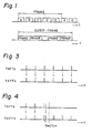
- Fig. 1 shows the timing location (map) of communication signals from stations in a TDMA system.
- the horizontal axes indicate time (t).
- Burst signals A, B, C, D and E from the stations are located with the time sharing arrangement shown by the blocks in Fig. 1.
- the burst signals A to E for example, form one frame.
- the lower portion of Fig. 1 shows a super- frame.
- a super-frame consists of a plurality of the above frames (e.g., 25), i.e., is an assembly of such frames in a larger unit, and transmits, for example, information regarding the burst signal location map.
- Fig. 2 shows a redundant transmission (TX) synchronization circuit in TDMA communication equipment.
- TX synchronization circuit 1a comprises a TX synchronization correction controller 11a, a selector 12a, a TX frame counter 13a, and a TX super-frame counter 14a.
- Another TX synchronization circuit 1 comprises the same elements as the TX synchronization circuit 1a, referenced with the same numbers but with the suffix "b". When one circuit fails, the other circuit takes over the operation.
- the circuit shown in the upper portion of Figs. 2 and 5 is referred to as the "active circuit” and the circuit shown in the lower portion of Figs. 2 and 5 as the "standby circuit.”
- the TX frame counter 13a counts a clock signal CKa, generated by a clock signal generator (not shown) contained in each TX synchronization circuit, and outputs a TX frame timing signal when the count reaches a predetermined value.
- the TX frame timing signal is supplied to the TX super-frame counter 14a and the TX synchronization correction controller 11 a as a frame trigger signal.
- the output of the TX synchronization correction controller 11 a is fed back to the TX frame counter 13a through the selector 12a and resets the count.
- the selector 12a is switched by a switching signal Sa from a redundant circuit switching controller (not shown), and the output of the TX synchronization correction controller 11 a is switched to the TX frame counter 13a, as mentioned above.
- the TX synchronization correction 11a receives a synchronization correction signal Ca from a TDMA synchronization controller (not shown) and corrects the deviation between a reference burst signal (e.g. block A in Fig. 1) and the TX frame timing signal from the TX frame counter 13a.
- the same operation is effected, except that the state of the selector 12b differs.
- the selector 12b is switched so that the output of the TX synchronization correction controller 11a is supplied to the TX frame counter 13b. Therefore, while the TX frame counter 13b counts its own clock signal CKb and outputs a TX frame timing signal when the count reaches a predetermined value, it is reset by the signal of the active circuit 1a.
- Fig. 3 shows the timing relationship between an active TX frame timing signal TXFTa and a standby TX frame timing signal TXFTb.
- the phases of the active and the standby TX frame timing signals are made to coincide at every frame timing signal (shown in Fig. 3 by arrows). Accordingly, synchronization coupling between the active TX frame timing signal and the standby TX frame signal is frequently performed. Therefore, there is no problem in switching from the active circuit 1a a to the standby circuit 1b when failure occurs at portions other than the TX synchronization circuits.
- the timing of the standby TX frame timing signal TXFTb also becomes abnormal. That is, as shown in Fig. 4, while the active TX frame signal TXFTa should have the timing shown by the broken line at time T1, if the active circuit fails and the timing of the active TX frame signal TXFTa becomes that shown by the solid line at time T1, the timing of the standby TX frame signal TXFTb also becomes that shown by the solid line. It takes a long time to correct the error after the switching from the active circuit 1a to standby circuit 1 b is carried out.
- FIG. 5 is a block circuit diagram of a TX synchronization circuit in redundant TDMA communication equipment according to an embodiment of the present invention.
- TX synchronization circuit 2a and a TX synchronization circuit 2b comprise the same elements.
- the active circuit 2a comprises a TX frame counter 13a for receiving and counting a clock signal CKa, a TX super-frame counter 14a for receiving and counting the output of the TX frame counter 13a and for generating a TX super-frame timing signal TXSFTa when the count reaches a predetermined value, a TX synchronization correction controller 11a for receiving the output of the TX frame counter 13a and a synchronization correction signal Ca from a TMDA synchronization controller (not shown), a selector 12a for receiving the output of the TX synchronization correction controller 11a at one input terminal thereof, a TX frame timing inhibit gate 21a for receiving the output of the TX frame counter 13a, an OR gate 22a for receiving the output of the inhibit gate 21 a at one input terminal thereof and for supplying the output to the other input terminal of the selector 12a, and a delay circuit 23a for supplying the output to the other input terminal of the OR gate 22a.
- the standby circuit 2b includes the same elements as the active circuit 2a. These elements are referenced by the same numbers but with suffixes "b".
- the output of the TX super-frame counter 14a is connected to the control terminal of the inhibit gate 21b and the input terminal of the delay circuit 23b, and the output of the TX super-frame counter 14b is connected to the control terminal of the inhibit gate 21a and the input terminal of the delay circuit 23a, as interconnections between the active circuit 2a and the standby circuit 2b.
- Switching signals Sa and Sb from a redundant circuit switching controller are connected to control terminals of the selector 12a and 12b, respectively.
- the output of the TX synchronization correction controller 11a is supplied to the TX frame counter 13a
- the output of the OR gate 22b is supplied to the TX frame counter 13b.
- the TX frame counter 13a counts the clock signal CKa from a clock signal generator (not shown) included in each TX synchronization circuit and outputs TX frame timing signal TXFTa when the count reaches a predetermined value.
- the TX frame timing signal TXFTa acts as a trigger signal for the TX super-frame counter 14a.
- the TX super-frame counter 14a When the TX super-frame counter 14a has counted a predetermined number of trigger signals, it outputs the TX super-frame timing signal TXSFTa.
- the TX frame timing signal acts as a trigger signal to reset the TX frame counter 13a, through the TX synchronization correction controller 11a and the selector 12a.
- the TX synchronization correction controller 11a includes a delay circuit (not shown) using a plurality of stages of flip-flop circuits. The delay time is controlled by the selection of the stages by the synchronization correction signal CA. As a result, synchronization between the reference burst signal and the TX frame timing signal is accomplished.
- the output of the active TX super-frame counter 14a namely, the TX super-frame timing signal
- the TX frame counter 13b runs independently from its own TX frame timing signal TXFTb in a "flywheel" operation.
- the inhibit gates 21a and 21b also include delay circuits having delay times corresponding to the delay times of the TX synchronization correction controllers 11 a and 11b.
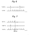
- the relation between the active TX super-frame timing signal TXSFTa and the standby TX frame timing signal TXFTb is shown in Fig. 6.
- the phase of the standby TX frame timing signal TXFTb coincides with the phase of the active TX super- frame timing signal TXSFTa when the active TX super-frame timing signal TXSFTa is being supplied.
- the TXframe counter 13b counts its own clock signal CKb. In the above-mentioned embodiment, the standby TX frame counter 13b is triggered only for each super-frame.
- the standby TX frame counter 13b effects a flywheel operation. This means less frequent coupling with the active circuit 2a compared with the conventional system and, consequently, less likelihood of the standby circuit 2b being affected by failure of the active circuit 2a.
- failure is detected in the active circuit 2a, synchronization of transmission signals is maintained by switching to the standby circuit 2b.
- This aspect is shown in Fig. 7. Even if the active TX frame timing signal TXFTa which should have the timing shown by the broken line has the timing shown by the solid line at time T2, the standby TX frame timing signal TXFTb continues at the normal timing since it is independent running except when the active TX super-frame signal TXSFTa is supplied to the standby TX frame counter 13b. Therefore, a normal synchronized TX frame timing signal can be obtained continuously by switching to the standby circuit 2b at an instant shown by the chain line.
- the TX superframe counters are used both for their inherent function and for triggering the standby TX frame counter. It is also possible, however, to replace the TX superframe counters with frequency dividers or to provide separate frequency dividers in addition to the counters to supply a frequency divided signal of one TX frame counter as a trigger signal to the other TX frame counter.
- the frequency divided signal may be selected so that the timing is appropriate (longer) to give less frequent coupling of the standby circuit to the active circuit.
Landscapes
- Engineering & Computer Science (AREA)
- Computer Networks & Wireless Communication (AREA)
- Signal Processing (AREA)
- Time-Division Multiplex Systems (AREA)
- Synchronisation In Digital Transmission Systems (AREA)
- Radio Relay Systems (AREA)
Claims (3)
Applications Claiming Priority (2)
| Application Number | Priority Date | Filing Date | Title |
|---|---|---|---|
| JP205977/82 | 1982-11-26 | ||
| JP57205977A JPS5997245A (ja) | 1982-11-26 | 1982-11-26 | 二重化された時分割多元接続方式の通信装置における同期方式 |
Publications (2)
| Publication Number | Publication Date |
|---|---|
| EP0110648A1 EP0110648A1 (de) | 1984-06-13 |
| EP0110648B1 true EP0110648B1 (de) | 1987-03-18 |
Family
ID=16515845
Family Applications (1)
| Application Number | Title | Priority Date | Filing Date |
|---|---|---|---|
| EP83307099A Expired EP0110648B1 (de) | 1982-11-26 | 1983-11-21 | Anordnung zur Synchronisation in einer redundanten Vielfachzugriff-Zeitmultiplex-Übertragungseinrichtung |
Country Status (4)
| Country | Link |
|---|---|
| US (1) | US4574377A (de) |
| EP (1) | EP0110648B1 (de) |
| JP (1) | JPS5997245A (de) |
| DE (1) | DE3370424D1 (de) |
Families Citing this family (17)
| Publication number | Priority date | Publication date | Assignee | Title |
|---|---|---|---|---|
| JPS60240278A (ja) * | 1984-05-15 | 1985-11-29 | Setsutaka Tomochika | 分割区域値のコ−ド化方法 |
| JPS60239881A (ja) * | 1984-05-15 | 1985-11-28 | Setsutaka Tomochika | 分割区域値のコ−ド化方法 |
| JPS60239880A (ja) * | 1984-05-15 | 1985-11-28 | Setsutaka Tomochika | 分割区域値のコ−ド化方法 |
| JPS60239879A (ja) * | 1984-05-15 | 1985-11-28 | Setsutaka Tomochika | 分割区域値のコ−ド化方法 |
| US4882738A (en) * | 1987-06-25 | 1989-11-21 | Nec Corporation | Clock control system |
| US4922489A (en) * | 1987-10-23 | 1990-05-01 | Siemens Aktiengesellschaft | Circuit configuration for routine testing of the clock supply of a large number of units operated with the same clock |
| US5376928A (en) * | 1992-09-18 | 1994-12-27 | Thomson Consumer Electronics, Inc. | Exchanging data and clock lines on multiple format data buses |
| JP2511370B2 (ja) * | 1993-02-26 | 1996-06-26 | 富士通株式会社 | 受信回路 |
| GB9414331D0 (en) * | 1994-07-15 | 1994-09-07 | Thomson Consumer Electronics | Combined I*C and IM bus architecture |
| JP3622510B2 (ja) | 1998-06-19 | 2005-02-23 | 富士通株式会社 | ディジタル加入者線伝送方法、adslトランシーバ、チャンネルアナリシステ方法及びadsl装置 |
| DE19832440A1 (de) * | 1998-07-18 | 2000-01-20 | Alcatel Sa | Synchronisationsverfahren, primärer Referenztaktgenerator und Netzelement für ein synchrones digitales Nachrichtenübertragungsnetz |
| JP3575998B2 (ja) * | 1998-08-28 | 2004-10-13 | 富士通株式会社 | フレーム同期処理装置及びフレーム同期処理方法 |
| JP4207329B2 (ja) * | 1999-09-20 | 2009-01-14 | 富士通株式会社 | フレーム同期回路 |
| US6728535B2 (en) | 2001-05-02 | 2004-04-27 | The Boeing Company | Fail-over of forward link equipment |
| SE0201008D0 (sv) * | 2002-04-03 | 2002-04-03 | Teracom Ab | A method and a system for synchronising digital data streams |
| US6970045B1 (en) | 2003-06-25 | 2005-11-29 | Nel Frequency Controls, Inc. | Redundant clock module |
| US8747387B2 (en) * | 2005-10-11 | 2014-06-10 | Covidien Lp | IV catheter with in-line valve and methods related thereto |
Family Cites Families (11)
| Publication number | Priority date | Publication date | Assignee | Title |
|---|---|---|---|---|
| US3795872A (en) * | 1972-09-18 | 1974-03-05 | Bell Telephone Labor Inc | Protection scheme for clock signal recovery arrangement |
| US3803568A (en) * | 1973-04-06 | 1974-04-09 | Gte Automatic Electric Lab Inc | System clock for electronic communication systems |
| US3974333A (en) * | 1975-09-24 | 1976-08-10 | Bell Telephone Laboratories, Incorporated | Adaptive synchronization system |
| US4019143A (en) * | 1976-05-10 | 1977-04-19 | Bell Telephone Laboratories, Incorporated | Standby apparatus for clock signal generators |
| JPS5346216A (en) * | 1976-10-08 | 1978-04-25 | Nec Corp | Time sharing multiplex commnicating unit |
| US4144448A (en) * | 1977-11-29 | 1979-03-13 | International Business Machines Corporation | Asynchronous validity checking system and method for monitoring clock signals on separate electrical conductors |
| JPS5582550A (en) * | 1978-12-15 | 1980-06-21 | Fujitsu Ltd | Digital radio unit |
| DE2907608A1 (de) * | 1979-02-27 | 1980-08-28 | Siemens Ag | Schaltungsanordnung zur takterzeugung in fernmeldeanlagen, insbesondere zeitmultiplex-digital-vermittlungsanlagen |
| US4282493A (en) * | 1979-07-02 | 1981-08-04 | Motorola, Inc. | Redundant clock signal generating circuitry |
| JPS5631248A (en) * | 1979-08-22 | 1981-03-30 | Fujitsu Ltd | Synchronizing system |
| JPS5689148A (en) * | 1979-12-21 | 1981-07-20 | Fujitsu Ltd | Radio device of switching without instantaneous break |
-
1982
- 1982-11-26 JP JP57205977A patent/JPS5997245A/ja active Granted
-
1983
- 1983-11-18 US US06/553,073 patent/US4574377A/en not_active Expired - Lifetime
- 1983-11-21 EP EP83307099A patent/EP0110648B1/de not_active Expired
- 1983-11-21 DE DE8383307099T patent/DE3370424D1/de not_active Expired
Also Published As
| Publication number | Publication date |
|---|---|
| EP0110648A1 (de) | 1984-06-13 |
| US4574377A (en) | 1986-03-04 |
| DE3370424D1 (en) | 1987-04-23 |
| JPS5997245A (ja) | 1984-06-05 |
| JPH0119781B2 (de) | 1989-04-13 |
Similar Documents
| Publication | Publication Date | Title |
|---|---|---|
| EP0110648B1 (de) | Anordnung zur Synchronisation in einer redundanten Vielfachzugriff-Zeitmultiplex-Übertragungseinrichtung | |
| EP0365819B1 (de) | Synchronisierte fehlertolerante Uhren für Multiprozessorsysteme | |
| EP0333196B1 (de) | Verstärker zur Regenerierung eines rahmenmultiplexierten Signals | |
| US5426633A (en) | System for processing synchronization signals with phase synchronization in a mobile communication network | |
| HUT58172A (en) | Synchronizing process for wireless systems | |
| US5920557A (en) | Radio base station inter-station synchronizing circuit | |
| US3936604A (en) | Synchronization of clocks in digital signalling networks | |
| JPH09139973A (ja) | 多重セル通信システムのフレーム同期方法および回路装置 | |
| US6683848B1 (en) | Frame synchronization and fault protection for a telecommunications device | |
| US6900683B2 (en) | Apparatus and method for generating a predetermined time delay in a semiconductor circuit | |
| US6163526A (en) | Transmission system for switching connection from a working channel line to a protection channel line while avoiding instantaneous cutoff upon failure | |
| US4355386A (en) | Time-division multiplex digital switching network for a PCM telephone exchange system utilizing duplicate connecting field installations | |
| US5778188A (en) | System for controlling delays in a ring by assembling subframes with a variable-delay by a master node, and with a fixed-delay by other nodes | |
| JPH021479B2 (de) | ||
| JP2007104143A (ja) | 伝送装置 | |
| JPH10145848A (ja) | Tdma移動体通信の基地局間フレーム同期方法 | |
| EP0282229B1 (de) | Synchronisieranordnung für eine digitale Fernmeldeanlage | |
| JPS5941335B2 (ja) | デイジタル無線回線切替方式 | |
| JP2693755B2 (ja) | 回線切替回路 | |
| JPH03154450A (ja) | ディジタル装置の同期方式 | |
| JPH0650834B2 (ja) | 時分割多元接続衛星通信方式 | |
| JPH01300727A (ja) | Tdma無線通信方式 | |
| JPH0531968B2 (de) | ||
| JPH02128544A (ja) | 送信マスタの決定方式 | |
| JP2000013366A (ja) | クロック切替回路 |
Legal Events
| Date | Code | Title | Description |
|---|---|---|---|
| PUAI | Public reference made under article 153(3) epc to a published international application that has entered the european phase |
Free format text: ORIGINAL CODE: 0009012 |
|
| AK | Designated contracting states |
Designated state(s): DE FR GB IT NL |
|
| 17P | Request for examination filed |
Effective date: 19840829 |
|
| GRAA | (expected) grant |
Free format text: ORIGINAL CODE: 0009210 |
|
| AK | Designated contracting states |
Kind code of ref document: B1 Designated state(s): DE FR GB IT NL |
|
| REF | Corresponds to: |
Ref document number: 3370424 Country of ref document: DE Date of ref document: 19870423 |
|
| ET | Fr: translation filed | ||
| ITF | It: translation for a ep patent filed |
Owner name: STUDIO JAUMANN |
|
| PLBE | No opposition filed within time limit |
Free format text: ORIGINAL CODE: 0009261 |
|
| STAA | Information on the status of an ep patent application or granted ep patent |
Free format text: STATUS: NO OPPOSITION FILED WITHIN TIME LIMIT |
|
| 26N | No opposition filed | ||
| ITTA | It: last paid annual fee | ||
| PGFP | Annual fee paid to national office [announced via postgrant information from national office to epo] |
Ref country code: FR Payment date: 19951109 Year of fee payment: 13 |
|
| PGFP | Annual fee paid to national office [announced via postgrant information from national office to epo] |
Ref country code: GB Payment date: 19951113 Year of fee payment: 13 |
|
| PGFP | Annual fee paid to national office [announced via postgrant information from national office to epo] |
Ref country code: DE Payment date: 19951128 Year of fee payment: 13 |
|
| PGFP | Annual fee paid to national office [announced via postgrant information from national office to epo] |
Ref country code: NL Payment date: 19951129 Year of fee payment: 13 |
|
| PG25 | Lapsed in a contracting state [announced via postgrant information from national office to epo] |
Ref country code: GB Effective date: 19961121 |
|
| PG25 | Lapsed in a contracting state [announced via postgrant information from national office to epo] |
Ref country code: NL Effective date: 19970601 |
|
| GBPC | Gb: european patent ceased through non-payment of renewal fee |
Effective date: 19961121 |
|
| PG25 | Lapsed in a contracting state [announced via postgrant information from national office to epo] |
Ref country code: FR Effective date: 19970731 |
|
| NLV4 | Nl: lapsed or anulled due to non-payment of the annual fee |
Effective date: 19970601 |
|
| PG25 | Lapsed in a contracting state [announced via postgrant information from national office to epo] |
Ref country code: DE Effective date: 19970801 |
|
| REG | Reference to a national code |
Ref country code: FR Ref legal event code: ST |