EP0365819B1 - Synchronisierte fehlertolerante Uhren für Multiprozessorsysteme - Google Patents
Synchronisierte fehlertolerante Uhren für Multiprozessorsysteme Download PDFInfo
- Publication number
- EP0365819B1 EP0365819B1 EP89117154A EP89117154A EP0365819B1 EP 0365819 B1 EP0365819 B1 EP 0365819B1 EP 89117154 A EP89117154 A EP 89117154A EP 89117154 A EP89117154 A EP 89117154A EP 0365819 B1 EP0365819 B1 EP 0365819B1
- Authority
- EP
- European Patent Office
- Prior art keywords
- tod
- reference frequency
- signal
- clock
- register
- Prior art date
- Legal status (The legal status is an assumption and is not a legal conclusion. Google has not performed a legal analysis and makes no representation as to the accuracy of the status listed.)
- Expired - Lifetime
Links
Images


Classifications
-
- G—PHYSICS
- G06—COMPUTING; CALCULATING OR COUNTING
- G06F—ELECTRIC DIGITAL DATA PROCESSING
- G06F1/00—Details not covered by groups G06F3/00 - G06F13/00 and G06F21/00
- G06F1/04—Generating or distributing clock signals or signals derived directly therefrom
- G06F1/14—Time supervision arrangements, e.g. real time clock
-
- G—PHYSICS
- G06—COMPUTING; CALCULATING OR COUNTING
- G06F—ELECTRIC DIGITAL DATA PROCESSING
- G06F11/00—Error detection; Error correction; Monitoring
- G06F11/07—Responding to the occurrence of a fault, e.g. fault tolerance
- G06F11/16—Error detection or correction of the data by redundancy in hardware
- G06F11/1604—Error detection or correction of the data by redundancy in hardware where the fault affects the clock signals of a processing unit and the redundancy is at or within the level of clock signal generation hardware
-
- G—PHYSICS
- G06—COMPUTING; CALCULATING OR COUNTING
- G06F—ELECTRIC DIGITAL DATA PROCESSING
- G06F11/00—Error detection; Error correction; Monitoring
- G06F11/07—Responding to the occurrence of a fault, e.g. fault tolerance
- G06F11/16—Error detection or correction of the data by redundancy in hardware
- G06F11/20—Error detection or correction of the data by redundancy in hardware using active fault-masking, e.g. by switching out faulty elements or by switching in spare elements
Definitions
- the invention is related to a fault-tolerant synchronization system for time of the day or TOD clocks in a multiprocessor complex, having TOD register/counters each including a plurality of bits for storing data representative of the TOD clock values, where switching of a predetermined bit in said register/counters providing a syncpoint signal, and having a synchronization facility for comparing the TOD clock signals and for synchronizing the settings and the stepping rates of said TOD register/counters to provide synchronized TOD clock signals to processors of said processor complex.
- a data processing system comprising a number of individual computers it is known to synchronize the processing speed by storing a predetermined value in binary counters one of them included in each of the computers (USP 3 761 884).
- a synchronization signal is applied to a common line interconnecting all the computers from the computer which operates more rapidly than the other when reaching a predetermined value in its counter.
- the synchronization signal is used to set all counters to such predetermined value.
- a master clock arrangement including a first, a second and optionally a third phase-locked loop being controlled by a common master oscillator (GB-A 2 000 651). By such arrangement the number of master oscillator may be reduced.
- a significant aspect of operating a plurality of data processors in a multiprocessor system complex is the synchronization of the individual clocks associated therewith. For example, it is desirable and in fact, frequently necessary that the separate Time of Day (TOD) clocks of the coupled processors be synchronized if these processors are sharing Direct Access Storage Devices (DASD), the data contained upon DASD and other resources, or the processors are exchanging messages. It is known to synchronize multiple TOD clocks by comparing the TOD clock signals and setting the TOD clock counters included in each clock to a predetermined value (IBM System/370 Principles of Operation, 1984, IBM Form No. GA22-7000-9, pages 4-23 to 4-29).
- TOD Time of Day
- DASD Direct Access Storage Devices
- a known method for synchronizing clocks in a distributed computing system in the presence of faults perform a periodical resynchronization of the clocks to secure that the clocks of the processors included in the system never deviate by more than a some maximum amount (EP-A 0 135 764).
- Each processor ascertains whether a time value message is received within a current synchronization interval. If this is not the case, it broadcasts to all other processors a time value together with its signature. Otherwise it broadcasts the time value received and its signature to the other processors. In both cases each processor resets the time for the expected resynchronization and updates its local clock.
- the complex represents a valuable resource and the individual processors exhibit intrinsic isolation of failures to single machines, it is necessary that the chosen clock synchronization mechanism not behave as a coupled or common failure mechanism, whereby a single point of failure therein could bring the entire complex down.
- the synchronization mechanism of the present invention fills such a need.
- a fault tolerant synchronization mechanism comprised basically of dual redundant TOD clock synchronization sources, and a plurality of TOD slaves which serve as the TOD clocks in the respective processors of the system complex.
- Each of the redundant TOD clock sources distributes a TOD synchronization signal to one of the TOD slaves.
- each slave receives two synchronization signals.
- the TOD slaves include means for selecting a valid TOD signal from between the two signals and the slave uses such signal to maintain synchronization within the complex.
- the present invention provides an economical means of maintaining synchronism between the two sides of the duplexed TOD clock reference sources.
- the reference frequency signals, as well as other various status and data bits generated within one side of the TOD sources are encoded and transmitted to the other side of the TOD sources, and vice versa.
- the phase of the incoming reference frequency signal is compared to the phase of the reference signal generated within the given side.
- a difference in phase between the signals results in a phase error signal which, after suitable processing, is used to vary the given side's reference frequency in a direction to drive the perceived phase error toward zero.
- the present invention also provides an economical means of receiving a duplexed TOD time reference, and for trouble-free switching from one side of the TOD clock sources to the other side, when required for failure accommodation or operational convenience.
- each TOD slave receives two reference frequency signals from the respective sides of the TOD clock sources, and selects one of them. The selected signal drives a phase locked-loop in the TOD slave. Error detection means associated with the slave, monitor the incoming reference frequency signal. If a failure is detected, the slave is switched to the other incoming reference signal. In the event that frequency and phase lock cannot be maintained with either incoming signal, or both incoming signals have failed, a synchronization exception is raised in the associated processor.
- the present invention contemplates a quad system implementation for near perfect coverage of all single points of failure of the synchronization mechanism. This last implementation is compatible with the duplex distribution of reference frequency signals to each TOD slave as described hereinbefore.
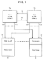
- a dual TOD synchronization system 10 comprised of a pair of identical TOD clock sources 12a and 12b, each of which generates a reference frequency signal.
- the sources are coupled to each other such that the reference frequency generated by one is transmitted to the other.
- the signal generated by source 12a is applied to source 12b via link 14, while the signal from source 12b is coupled to source 12a by link 16.
- the sources 12a and 12b provide respective pluralities of synchronization signals on lines 18 and 20.
- a pair of reference frequency signals, one from each of lines 18 and 20 are transmitted to a common TOD slave 22 associated with one of the processors 24 of the system complex.
- the TOD slaves 22 serve as the TOD clocks in the complex.
- the TOD sources 12a and 12b and the TOD slaves 22 may be coupled to one another by means of dedicated links, as in a dual star configuration, or by a dual redundant bus structure.
- each of the TOD slaves 22 selects one reference frequency signal from the pair of signals transmitted to it by the TOD sources 12a and 12b, and uses such signal to maintain synchronization within the complex.
- the reference frequency signal is a low enough frequency so that any skews between the two clock sources are small with respect to one period of the reference frequency.
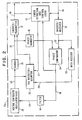
- Fig. 2 provides details of the internal organization of the elements of which TOD clock source 12a of Fig. 1 is comprised. It should be understood that TOD clock source 12b consists of like elements.
- a TOD register/counter 26 which represents a facsimile of the standard format TOD clock utilized by the particular processors in the complex, and as such, it has the same bit resolution as the latter.
- a 64 bit TOD register formal compatible with the IBM S/370 TOD will be assumed.
- the bits of the TOD are numbered from 0 to 63. Bit 0 is the most significant bit and bit 63 is the least.
- the register is a binary counter and is incremented at a rate which causes bit 31 of the register to toggle every 220 microsecond (approximately 1.04 seconds). This is called a mega-micro-second or MuS period.
- a voltage controlled oscillator (VCO) 28 generates the internal clock for the TOD source 12a.
- This internal clock is used to increment the TOD register/counter 26 and is also divided down in divider 30 to produce the TOD reference frequency for TOD source 12a.
- the period of the reference frequency is selected to be larger than any skews which may appear between sources 12a and 12b due to normal variations in component characteristics.
- the reference frequency is used as a carrier for the data. It should be noted that the actual resolution of the counter (the inherent VCO internal clock frequency) can be arbitrarily high with respect to this reference frequency.
- An encoder/transmitter 32 is provided for encoding and transmitting the TOD source 12a reference frequency, together with other status and data bits.
- a decoder/receiver 34 is provided for receiving and decoding the reference frequency and transmitted data from the other TOD source 12b (Fig. 1).
- phase adjuster 36 Also included in TOD source 12a are phase adjuster 36, phase comparator 38 and filter 40 circuits, and miscellaneous error detection and associated control elements 42.
- the VCO 28 provides an internal clock output signal on line 44 which is used to increment the TOD register/counter 26.
- the signal from the VCO 28 is also applied to divider 30, where it is divided down to produce a reference frequency signal.
- a synchronization point signal or "syncpoint" (the MuS syncpoint in this embodiment) is derived from the count in the TOD register/counter 26, as indicated hereinbefore.
- the reference frequency, syncpoint, and TOD register/counter 26 data and various status indicators are encoded and transmitted by encoder/transmitter 32 to TOD source 12b (Fig. 1) via line 46. As indicated in Fig. 1, all of the last mentioned information is transmitted as well to all of the TOD slave units 22 within the complex.
- the present invention contemplates the use of bi-phase encoding of the data and syncpoint at the reference frequency, with suitable sync, framing and idle symbols.
- the data transmission includes the value of bits 0:31 (high order bits) of the TOD register/counter 26 after the next syncpoint, and further includes various status bits.
- the transmission of the TOD register/counter value is chosen to be well away from the syncpoint transmission, so as to simplify its use at syncpoint with minimally complex control logic.
- the encoded transmission from the other TOD clock source 12b is received by TOD source 12a on line 48 and is applied to decoder/receiver 34, where it is decoded into a reference frequency, syncpoint, and data.
- the data is stored in an appropriate holding register 50 where it is available to the control logic for TOD source 12a.
- phase comparator 38 compares the phases of the two input signals and provides an output signal on line 56 which is the representative of the phase error therebetween.
- a suitable method for performing this phase comparison utilizes a simple exclusive-OR gate with averaging and filtering of its output.
- phase error signal on line 56 is processed utilizing first order lag dynamics with steady state gain K, as is implemented by filter 40.
- the output signal from filter 40 appearing on line 58 is applied to VCO 28, and operates to change its frequency in a direction to cause the phase error signal to approach zero.
- the TOD source 12a includes error detection circuits 42 which monitor the phase error between the incoming reference frequency signal on line 48 and the outgoing signal on line 46 and determines when phase lock is obtained, or when it is lost.
- the error detection circuits also function to detect other simple failures such as power out of regulation and complete loss of the input signal.
- the circuits 42 further provide consistency checks such as the correct number of cycles between syncpoints. These conditions operate to set various status flags which are included in the data being transmitted from a TOD clock source.
- phase of a signal is the integral of its frequency, and the system applies a first order filter to phase differences, it follows from classical control theory that the system as a whole is a second order system. For the whole fault-tolerant system to be stable under all failure modes, it is necessary that the parameters of the first order filter be chosen such that the second order system is overdamped. It should be noted that in stady state operation each of the TOD clock sources 12a and 12b of the duplex system will perceive a steady state phase error which is required to deflect that TOD source's intrinsic operating frequency to the steady state operating frequency. If the propagation delay phase compensation is perfect, this operating frequency will be the average of the two intrinsic operating frequencies.
- the operating frequency will also be partially determined by the magnitude of this error and the steady state gain K.
- the steady state result will be such that the TOD clock sources 12a and 12b are operating at exactly the same frequency but with some steady state phase error or skew between them.
- the maximum magnitude of this phase error can be computed as a function of implementation parameters; and the reference frequency should be such that this maximum steady state phase error is no more than 30 to 45 degrees of the reference frequency. It must be smaller than the performance boundary of the phase comparator being employed and should additionally include, engineering margins.
- the most commonly and economically implemented phase comparators operate over +/-90 degrees, but +/-180 degree comparators are also easily implemented and are within the state of the art.
- the TOD clocks and syncpoint can be aligned by having one of the TOD clock sources accept the TOD value and MuS syncpoint from the other clock source.
- the TOD value could be entered from either TOD clock source through a manual operation or from an external frequency reference standard, and the alternate TOD clock source could simply accept this value.
- one of the TOD clock sources is restarting, such as after repair or power interruption, it would accept the TOD value and syncpoint from the operating TOD source. It should be noted that under normal operating conditions, the two TOD clock sources 12a and 12b will maintain alignment with each other without adjustments of either the TOD value of the MuS syncpoint.
- a clock source should not attempt to realign itself with the other source, except in those cases where it has a positive indication of an internal fault such as a power on reset. It is therefore advantageous that discreet data should be transmitted as part of the data stream between the two TOD clock sources, to indicate whether a source believes that it is maintaining frequency lock, restarting, or other situation and whether it believes that its TOD value and syncpoint are valid.
- the accepting side To accept the syncpoint and TOD value from the other side the accepting side must first establish reference frequency phase lock. Once this is done, the control logic 42 inhibits TOD counter 26 via line 27, clearing those bits of the TOD counter 26 to zero below the syncpoint (bits 32 through 63 in the embodiment).
- control logic 42 waits until data register 50 has received the transmitted TOD value from decoder/receiver 34 for the higher order bits of the TOD counter and loads these via line 29 into the TOD counter above the syncpoint (bits 0 through 31 in the embodiment). The control logic 42 then waits until it receives the next syncpoint signal and reenables the TOD register/counter via line 27 at that syncpoint. At this time, the TOD register/counters are aligned to the skew accuracy of the reference signal.
- circuit elements which comprise the receiver 60 of the TOD slave 22 for the dual redundant broadcast clock embodiment.
- Such elements include the decoder/receiver units 62 and 64 for the pair of broadcast signals transmitted respectively by the TOD clock sources 12a and 12b.
- a phase-locked loop with its associated oscillator 66 is provided for driving a slave TOD register/counter 68.
- error detection and control logic circuits 70 are also included in the receiver circuit organization.
- the reference frequency signals from the TOD clock sources 12a and 12b are received on lines 18 and 20 and are decoded by decoder/receivers 62 and 64 into signals representative of a reference frequency, syncpoint event and data.
- the data is held in registers 72a and 72b for use by the control logic circuits 70.
- Either the reference frequency derived from TOD clock source 12a or clock source 12b is used to drive the TOD slave's phase-locked loop 66 which is coupled to the slave TOD register/counter 68 and increments the latter.
- the TOD clock source which provides the selected reference signal is referred to as the "primary”; the other clock source, "secondary”. It should be noted that the reference frequency on line 74 is too low to directly drive the slave TOD register/counter 68, and thus the slave phase-locked loop 66 is required to frequency multiply the reference frequency to the desired level to obtain the necessary TOD register/counter resolution, in the same fashion as described for the TOD clock source.
- the error detection circuits 70 are utilized to detect obvious failures of either incoming signal on lines 18 or 20, and are effective in switching the TOD slave 22 via select unit 71 to the secondary source when a failure of the primary is observed. Moreover, when the error detection circuits 70 are unable to maintain frequency and phase lock with a signal from either TOD clock source or both signals indicate a failed condition, they post a synchronization exception to the processor.
- the error detection circuits provide as a minimum, detection for complete loss of a signal from a clock source, phase or syncpoint misalignment either between the primary or secondary TOD clock sources and the TOD slave, phase or syncpoint misalignment between the TOD clock sources, and disagreement between the TOD clock sources and/or the slave TOD values.
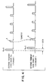
- Fig. 4 illustrates, by way of example, the failure of the reference frequency signal of clock source 12a at point "A”, and the transfer of TOD slave 22 to the "nearest" reference frequency pulse at point "B", generated within clock source 12b.
- the skew between the reference frequency pulses generated respectively within clock sources 12a and 12b must be small relative to the period of the reference frequency.
- the magnitude of the reference frequency is chosen to be low enough that adjacent reference frequency pulses occur relatively far apart. Accordingly, the transfer of the TOD slave 22 from clock source 12a to source 12b is achieved without any ambiguity as to the pulse from source 12b which is to be accepted by the slave.
- the next pulse from source 12b at point "B" occurring after the failure of source 12a at point “A” is the "correct” pulse from the standpoint of synchronization.
- the incrementation of the TOD slave register/counter 68 by the high frequency internal clock pulses is unaffected by the transfer from one clock source to the other. That is, none of the high frequency internal clock pulses applied to the register/counter 68 are lost in the transfer process.
- the TOD slave's clock and syncpoint can be aligned with one of the reference signals from TOD clock sources 12a or 12b by having it load the TOD bits 0:31, and inhibiting its own internal TOD register/counter 68 incrementation until the syncpoint signal is received.
- this synchronization process is controlled by the SETCLOCK instruction from the processor 24.
- the processor receives a signal on line 63 from select unit 71 to read via line 65a or 65b, the received TOD value from either data register 72a or 72b, containing data derived from the selected reference frequency carrier.
- the processor 24 then loads the data into the TOD slave register/counter 68 via line 67 with a SETCLOCK instruction. This instruction loads the TOD and inhibits the register/counter until a synchronization signal occurs. This signal is provided by the syncpoint signal.
- the alignment procedure should only be executed once during processor initialization, and only in conjunction with the above mentioned programming instruction of the processor. Once alignment is achieved, then a disagreement between the slave's TOD value syncpoint and the transmitted reference signals is an indication of a fault. If the slave's internal TOD value syncpoint differs from the primary TOD clock source reference frequency but agrees with the secondary, then the primary has failed and the slave must switch to the secondary reference. If both reference frequencies from the primary and secondary agree, but the slave's clock disagrees, then the slave's TOD clock should be assumed to have failed, and a synchronization exception must be raised in the processor.
- the TOD slave 22 may switch back and forth from the primary clock source to the secondary source without interfering with the integrity and alignment of its own TOD value. If necessary, the switchover may require a phase alignment of the oscillator in the phase-locked loop 66 and this can be accomplished without disturbing the slave's TOD value.
- the TOD slave 22 may select either one as the primary. Once selected, the slave may always return to this primary source, for example, after it has been taken out of service for a failure and is subsequently restored. It should be observed that the ability to easily switch from one source to the other requires that the sources have only small skews with respect to one another and the reference frequency.
- the error detection circuits 70 are necessary to detect failures in the reference frequency signals from the TOD clock sources. Such circuits may be implemented for example, by a simple monitor responsive to the power for the TOD sources. Thus, a power failure could be used to inhibit transmission of the reference clock frequency from the associated TOD clock source. A total failure of the oscillator in a clock source should have the same results. Other failures may also be easily detected, such an incorrect number of reference cycles between sync signals. Although many different failures may be detected and are generally tolerated by the duplex system, there are certain deficiencies in the system which cannot be detected.
- a solution to the inherent detection and fault isolation problems of a purely dual system requires additional frequency standards. Theory dictates 3f + 1 frequency sources to tolerate all single point failures. A quad implementation is therefore required to tolerate all single point failures. Conveniently, a quad implementation can be constructed which remedies the uncovered fault modes mentioned above, and which is compatible with the described duplex distribution scheme. Such a quad configuration is partitioned and packaged in two pieces creating a dual partition quad architecture. Such a system is illustrated i Fig. 5.
- Fig. 5 depicts four TOD clock sources 76a, 76b, 76c and 76d which are substantially the same as clock source 12a or 12b illustrated in Fig. 2.
- Each of the clock sources has a phase-locked loop (PLL).
- Clock sources 76a, 76b, 76c and 76d transmit respectively reference signals a, b, c and d to each of the other three sources.
- Each TOD clock source then votes (V) the received three signals and attempts to phase lock to the voted reference signal.
- V phase-locked loop
- Any two of the TOD clock sources can then be used to transmit dual reference signals 78 and 80 to the TOD slave 22 as in the case of the duplex system.
- clock sources 76c and 76d may be chosen as primary and secondary sources. Comparison circuits internal to a TOD clock source can easily detect the loss of phase lock by the transmitting source and can provide a failure indication which is easily detected by the TOD slave receiver 60. This detection forces the slave 22 to switch to the secondary source quickly enough to avoid breaking phase lock. It is apparent that except for the elimination of the so called "near correct frequency" failure modes of the purely dual structure of Fig. 1, the quad architecture of Fig. 5 has similar operational characteristics to the duplex structure.
- Fig. 6 illustrates a mechanism for frequency steering a TOD clock source 82 of either the dual or quad configurations.
- a summing circuit 84 is interposed between the filter 40 and oscillator 28. The output of the summing circuit 84 on line 86 is applied to the VCO 28 and controls the output frequency thereof.
- the TOD clock value is stored in the TOD register/counter 26.
- a precise time reference 88 is utilized. The signals from the TOD register/counter 26 and the precise time reference 88 are applied to a compute trim correction circuit 90 where they are compared. Deviations in the frequencies of the compared signals cause the trim correction circuit 90 to generate a steering signal on line 92.
- This signal is applied to an authority filter 94, the function of which is to limit the magnitude of the trim adjustment provided by the steering signal so that it is not so great as to force a break in phase lock among the synchronized components of the system.
- the output of the authority filter 94 is summed with the processed error signal from filter 40 in summing circuit 84.
- the output of the summing circuit 84 will cause the VCO output frequency to be deflected downward or upward.
- the remaining elements of TOD clock source 82 function in the same manner as the like-named numbered of Fig. 2.
- the integrity of synchronization is uncoupled from the accuracy of the TOD clock.
- the steering mechanism need not be continuous since the normal synchronization of the TOD clock source 82 can be adequately maintained for long periods of time without diverging from real time significantly. Accordingly the precise time reference does not need to be continuously available.
- a radio based frequency standard such as WWV could be utilized intermittently, or alternately the precise frequency reference 88 may simply be a fixed frequency oscillator with manual corrections to the time when significant deviations are noted.
- the value of the reference frequency has a significant effect on the encode/transmitter and decode/receiver logic as well as the nature of the distribution of the reference signals. For example, if synchronization requirements dictate skews of less than one microsecond, then a reference frequency near 10 to 100 KHz. is appropriate.
- Twisted wire distribution of such a low frequency is adequate for star topologies, and coaxial or twinax may be used for buses.
- skews of less than one microsecond will require more judicious management of cable lengths, as cable propagation delays are significant relative to this skew requirement. If the application allows 10 or 20 microsecond skews, then the reference frequency below 1 KHz and twisted pairs with only coarse management of cable length will be adequate.
Landscapes
- Engineering & Computer Science (AREA)
- Theoretical Computer Science (AREA)
- Physics & Mathematics (AREA)
- General Engineering & Computer Science (AREA)
- General Physics & Mathematics (AREA)
- Hardware Redundancy (AREA)
- Stabilization Of Oscillater, Synchronisation, Frequency Synthesizers (AREA)
- Synchronisation In Digital Transmission Systems (AREA)
Claims (13)
- Fehlertolerantes Synchronisationssystem für Tageszeit- oder TOD-Uhren in einem Multiprozessorkomplex mit TOD-Registern/Zählern, von denen jedes/jeder eine Vielzahl von Bits zum Speichern von Daten, die für die TOD-Uhrwerte repräsentativ sind, enthält, wobei das Schalten eines vorbestimmten Bits in den Registern/Zählern ein Synchronpunktsignal liefert, und mit einer Synchronisationseinrichtung zum Vergleichen der TOD-Uhrsignale und zum Synchronisieren der Einstellungen und Schrittraten der TOD-Register/Zähler, um den Prozessoren des Prozessorkomplexes synchronisierte TOD-Uhrsignale bereitzustellen, gekennzeichnet durch:
wenigstens ein Paar von gleichen TOD-Uhrquellen (12a, 12b), die in einer Doppelkonfiguration angeordnet sind, wobei jede der Uhrquellen enthält;
Mittel (28) zum Erzeugen eines internen Uhrsignals mit einer vorbestimmten Frequenz,
TOD-Register/Zähler (26), gekoppelt an das Erzeugungsmittel, wobei das interne Uhrsignal an Register/Zähler angelegt wird, um letzteren mit der Rate der vorbestimmten Frequenz zu inkrementieren,
an das Erzeugungsmittel gekoppelte Mittel (30) zum Teilen der vorbestimmten Frequenz, um ein Referenzsignal niedrigerer Frequenz für Synchronisationszwecke bereitzustellen,
gemeinsames an das Teilungsmittel und Register/Zähler gekoppeltes Mittel (32) zum Übertragen des Referenzsignals niedrigerer Frequenz an die anderen der TOD-Uhrquellen, wobei das Referenzsignal niedrigerer Frequenz als ein Träger für das Übertragen von das Synchronpunktsignal und die TOD-Uhrwertedaten enthaltender Information an die anderen der Uhrquellen dient, und
Mittel (34) zum Empfangen des Referenzsignals niedrigerer Frequenz und der Information von den anderen der Uhrquellen. - Fehlertolerantes Synchronisationssystem wie in Anspruch 1 angegeben,
das darüber hinaus in jeder der TOD-Uhrquellen (12a, 12b) Mittel zum Vergleichen der jeweiligen Phasen der übertragenen und empfangenen Referenzsignale niedrigerer Frequenz und zum Erzeugen eines Fehlersignals enthält und
Filtermittel (40) zum Verarbeiten des Fehlersignals und zum Anlegen eines Ausgangssignals an das Erzeugungsmittel (28), um die vorbestimmte Frequenz und das davon abgeleitete Referenzsignal niedrigerer Frequenz in eine Richtung zu verändern, um zu bewirken, daß das Fehlersignal Null erreicht. - Fehlertolerantes Synchronisationssystem wie in Anspruch 1 oder 2 angegeben, dadurch gekennzeichnet, daß das Paar von TOD-Uhrquellen (12a, 12b) bei derselben Referenzfrequenz arbeitet, aber untereinander eine Abweichung im eingeschwungenen Zustand aufweist, wobei der Wert der Referenzfrequenz derart gewählt ist, daß seine Periode größer als die Abweichung im eingeschwungenen Zustand ist.
- Fehlertolerantes Synchronisationssystem wie in Anspruch 3 angegeben, darüber hinaus dadurch gekennzeichnet, daß der Wert der vorbestimmten Frequenz derart gewählt ist, daß eine vorgewählte hohe Auflösung des Registers/Zählers (26) im Hinblick auf die Referenzfrequenz realisiert ist.
- Fehlertolerantes Synchronisationssystem wie in einem der Ansprüche 1 bis 4 angegeben, wobei die Mittel (32, 34) zum Übertragen und Empfangen des Referenzsignals niedrigerer Frequenz und der zugeordneten Information Coder-/Sendermittel bzw. Decoder-/Empfängermittel umfassen und
ein Halteregister (50), das an das Decoder-/Empfängermittel (34) zum Speichern der Daten gekoppelt ist. - Fehlertolerantes Synchronisationssystem wie in einem der Ansprüche 1 bis 5 angegeben, das darüber hinaus Steuerlogikmittel (42) enthält, das in jeder der TOD-Uhrquellen (12a, 12b) an TOD-Register/Zähler (26) gekoppelt ist, um dessen Initialisierung zu bewirken,
ein erstes Steuerlogikmittel zum Verhindern des Inkrementierens eines ersten Registers/Zählers in einer ersten der Uhrquellen, der mit einem zweiten Register/Zähler in einer zweiten der Uhrquellen abzugleichen ist,
wobei das erste Steuerlogikmittel die niedrigerwertigen Bits des ersten Registers/Zählers, die unterhalb des dem Synchronpunktsignal zugeordneten vorbestimmten Bits liegen, löscht und wobei das erste Steuerlogikmittel die von dem zweiten Register/Zähler empfangenen höherwertigen Bits, die oberhalb des vorbestimmten Bits liegen und im Halteregister der ersten Uhrquelle gespeichert sind, in den ersten Register/Zähler liest,
wobei das erste Steuerlogikmittel auf das Auftreten des nächsten Synchronpunktsignals von der zweiten Uhrquelle antwortet, um den ersten Register/Zähler wieder freizugeben, wodurch die ersten und zweiten Register/Zähler im wesentlichen zum Abgleich gebracht werden. - Fehlertolerantes Synchronisationssystem wie in Ansprüchen 1, 2 und 4 bis 6 angegeben, das darüber hinaus Frequenzsteuerungsmittel enthält, die umfassen:
eine Zeitreferenz (88),
Rechentrimmkorrekturmittel (90) mit einem Paar von Eingangsanschlüssen und einem Ausgangsanschluß (92),
Mittel zum Koppeln von Signalen von der Zeitreferenz bzw. dem TOD-Register/Zähler an das Paar von Eingangsanschlüssen des Rechentrimmkorrekturmittels, wobei das Rechentrimmkorrekturmittel die zuletzt angegebenen Signale vergleicht und ein Steuersignal an seinem Ausgangsanschluß proportional zur Differenz der Frequenzen der zuletzt angeführten Signale erzeugt,
Summiermittel (84) mit einem Paar von Eingangsanschlüssen und einem Ausgangsanschluß,
Billigungsfiltermittel (94), das zwischen dem Ausgangsanschluß das Rechentrimmkorrekturmittels und einem des Paars von Eingangsanschlüssen des Summiermittels angeordnet ist, wobei das Billigungsfiltermittel die Größe des Steuersignals begrenzt, um eine Unterbrechung in der Phasenrastung in der Uhrquelle auszuschließen,
wobei das verarbeitete Fehlersignal vom Filtermittel (40) an das andere Eingangssignal des Summiermittels angelegt wird,
wobei der Ausgangsanschluß des Summiermittels an den Eingangsanschluß des Erzeugungsmittels (28) gekoppelt ist, das resultierende Signal vom Summiermittel an dessen Ausgangsanschluß erscheint und bewirkt, daß die Frequenz des Erzeugungsmittels zur Übereinstimmung mit der Frequenz der Zeitreferenz führt. - Fehlertolerantes Synchronisationssystem wie einem der Ansprüche 1 bis 7 angegeben, das darüber hinaus enthält:
eine Vielzahl von TOD-Slaves (22), die jeweils den Prozessoren (24) des Komplexes zugeordnet sind,
wobei das Paar der TOD-Uhrquellen (12a, 12b) die Referenzfrequenzsignale jeweils an jeden der TOD-Slaves überträgt,
wobei jeder der TOD-Slaves ein Paar von Decodern/Empfängern (62, 64) zum jeweiligen Empfangen der Referenzfrequenzsignale von dem Paar der TOD-Uhrquellen aufweist,
Mittel (71) zum Auswählen eines der Referenzsignale niedrigerer Frequenz und Mittel (66, 68), die auf das ausgewählte Referenzsignal niedrigerer Frequenz antworten, um eine TOD-Uhr zur Benutzung durch ihren zugeordneten Prozessor bereitzustellen. - Fehlertolerantes Synchronisationssystem wie in Anspruch 8 festgelegt, das ein Paar von Datenregistern (72a, 72b) enthält, die jeweils an die Decoder/Empfänger (62, 64) gekoppelt sind, um die Daten von den Registern/Zählern des Paars von Uhrquellen (12a, 12b) zu speichern.
- Fehlertolerantes Synchronisationssystem wie in Anspruch 8 oder 9 festgelegt, dadurch gekennzeichnet, daß das Mittel (71) zum Auswählen eines der Referenzsignale niedrigerer Frequenz enthält,
Fehlererkennungsmittel, das im Betrieb an die beiden Referenzsignale niedrigerer Frequenz gekoppelt ist, um deren Zustand zu überwachen,
Signalauswahlmittel (71), das an das Fehlererkennungsmittel gekoppelt ist und darauf anspricht, um das Mittel zum Bereitstellen der TOD-Uhr wahlweise an eines der Referenzsignale niedrigerer Frequenz zu koppeln,
wobei die Erkennung eines Fehlers in dem an einen TOD-Slave gekoppelten Referenzsignal niedrigerer Frequenz zu irgendeiner gegebenen Zeit durch das Fehlererkennungsmittel bewirkt, daß das Signalauswahlmittel das Mittel zum Bereitstellen der TOD-Uhr an das andere der Referenzsignale niedrigerer Frequenz umschaltet, um dadurch einen Verlust von Synchronisation im Multiprozessorkomplex zu verhindern. - Fehlertolerantes Synchronisationssystem wie in einem der Ansprüche 8 bis 10 festgelegt, wobei die Mittel (66, 68) zum Bereitstellen einer TOD-Uhr zur Benutzung durch ihren zugeordneten Prozessor einen in einer Phasenregelschleife angeordneten Oszillator (66) enthalten,
Slave-TOD-Register/Zähler (68), gekoppelt an den Oszillator, um den Wert der TOD-Uhr zu speichern, wobei der Oszillator Slave-TOD-Register/Zähler mit einer vorbestimmten Rate inkrementiert,
wobei das Signalauswahlmittel (71) an den Oszillator gekoppelt ist, wobei der Oszillator durch das ausgewählte des Paars von Referenzsignalen niedrigerer Frequenz, die durch die Uhrquellen an Decoder/Empfänger (62, 64) jedes der TOD-Slaves (22) übertragen werden, getrieben wird. - Fehlertolerantes Synchronisationssystem wie in einem der Ansprüche 1 bis 11 festgelegt, das darüber hinaus umfaßt:
ein erstes und ein zweites Paar von gleichen TOD-Uhrquellen (76a, 76b, 76c, 76d), die in einer Vierfachkonfiguration, die auf alle Einpunktfehler im wesentlichen unempfindlich ist, angeordnet sind, wobei jede der Uhrquellen enthält,
in einer Phasenregelschleife angeordnetes Mittel (PLL) zum Erzeugen eines internen Taktsignals mit einer vorbestimmten Frequenz,
TOD-Register/Zähler (26), das Erzeugungsmittel (28) und das Teilungsmittel (30),
gemeinsam an das Teilungsmittel und an Register/Zähler gekoppelte Mittel zum Übertragen des Referenzsignals niedrigerer Frequenz an jede der übrigen drei Uhrquellen, wobei das Referenzsignal niedrigerer Frequenz als ein Träger zum Übertragen von das Synchronpunktsignal und die TOD-Uhrwertedaten enthaltender Information an die drei Uhrquellen dient, und
Mittel zum jeweiligen Empfangen von Referenzsignalen niedrigerer Frequenz von den drei Uhrquellen,
Wählmittel zum Auswählen eines der dadurch empfangenen drei Referenzsignale niedrigerer Frequenz und
Mittel zum Anlegen des ausgewählten empfangenen Referenzsignals niedrigerer Frequenz an das Erzeugungsmittel (28), wobei die jeweiligen Phasen des übertragenen Referenzsignals niedrigerer Frequenz und des ausgewählten empfangenen Referenzfrequenzsignals in wesentliche Übereinstimmung gebracht werden. - Fehlertolerantes Synchronisationssystem wie in Anspruch 12 festgelegt, das enthält:
eine Vielzahl von TOD-Slaves, die jeweils den Prozessoren des Komplexes zugeordnet sind,
ein ausgewähltes Paar des ersten und zweiten Paars von TOD-Uhrquellen (76a, 76b, 76c, 76d), das die Referenzsignale niedrigerer Frequenz an jeden der TOD-Slaves überträgt,
wobei jeder TOD-Slave Mittel zum Empfangen des Paars von Referenzsignalen niedrigerer Frequenz und zum Auswählen eines davon enthält,
wobei jeder TOD-Slave darüber hinaus Mittel enthält, die auf das ausgewählte Referenzsignal niedrigerer Frequenz antworten, um eine TOD-Uhr zur Benutzung durch ihren zugeordneten Prozessor bereitzustellen.
Applications Claiming Priority (2)
| Application Number | Priority Date | Filing Date | Title |
|---|---|---|---|
| US26241688A | 1988-10-25 | 1988-10-25 | |
| US262416 | 1988-10-25 |
Publications (3)
| Publication Number | Publication Date |
|---|---|
| EP0365819A2 EP0365819A2 (de) | 1990-05-02 |
| EP0365819A3 EP0365819A3 (de) | 1991-09-18 |
| EP0365819B1 true EP0365819B1 (de) | 1995-08-16 |
Family
ID=22997411
Family Applications (1)
| Application Number | Title | Priority Date | Filing Date |
|---|---|---|---|
| EP89117154A Expired - Lifetime EP0365819B1 (de) | 1988-10-25 | 1989-09-16 | Synchronisierte fehlertolerante Uhren für Multiprozessorsysteme |
Country Status (4)
| Country | Link |
|---|---|
| US (1) | US5146585A (de) |
| EP (1) | EP0365819B1 (de) |
| JP (1) | JPH0797328B2 (de) |
| DE (1) | DE68923845T2 (de) |
Cited By (1)
| Publication number | Priority date | Publication date | Assignee | Title |
|---|---|---|---|---|
| US11940836B2 (en) | 2022-03-31 | 2024-03-26 | International Business Machines Corporation | Dual chip clock synchronization |
Families Citing this family (84)
| Publication number | Priority date | Publication date | Assignee | Title |
|---|---|---|---|---|
| US5041798A (en) * | 1990-06-12 | 1991-08-20 | International Business Machines Corporation | Time reference with proportional steering |
| US5504878A (en) * | 1991-02-04 | 1996-04-02 | International Business Machines Corporation | Method and apparatus for synchronizing plural time-of-day (TOD) clocks with a central TOD reference over non-dedicated serial links using an on-time event (OTE) character |
| US5636373A (en) * | 1991-09-04 | 1997-06-03 | International Business Machines Corporation | System for synchronizing logical clock in logical partition of host processor with external time source by combining clock adjustment value with specific value of partition |
| US5544180A (en) * | 1992-06-08 | 1996-08-06 | Qlogic Corporation | Error-tolerant byte synchronization recovery scheme |
| US5327468A (en) * | 1992-06-19 | 1994-07-05 | Westinghouse Electric Corp. | Synchronization of time-of-day clocks in a distributed processing network system |
| US5347227A (en) * | 1992-12-10 | 1994-09-13 | At&T Bell Laboratories | Clock phase adjustment between duplicated clock circuits |
| US5790776A (en) * | 1992-12-17 | 1998-08-04 | Tandem Computers Incorporated | Apparatus for detecting divergence between a pair of duplexed, synchronized processor elements |
| JPH06195147A (ja) * | 1992-12-23 | 1994-07-15 | Fujitsu Ltd | クロック制御装置 |
| US5509035A (en) * | 1993-04-14 | 1996-04-16 | Qualcomm Incorporated | Mobile station operating in an analog mode and for subsequent handoff to another system |
| US5870427A (en) * | 1993-04-14 | 1999-02-09 | Qualcomm Incorporated | Method for multi-mode handoff using preliminary time alignment of a mobile station operating in analog mode |
| SE501156C2 (sv) * | 1993-04-21 | 1994-11-28 | Ellemtel Utvecklings Ab | Referenssignal sammansatt av klocksignal och synkroniseringssignal, anordning och förfarande för synkronisering m.h.a. referenssignal |
| US5600822A (en) * | 1994-04-05 | 1997-02-04 | International Business Machines Corporation | Resource allocation synchronization in a parallel processing system |
| US5450458A (en) * | 1994-08-05 | 1995-09-12 | International Business Machines Corporation | Method and apparatus for phase-aligned multiple frequency synthesizer with synchronization window decoder |
| US5537583A (en) * | 1994-10-11 | 1996-07-16 | The Boeing Company | Method and apparatus for a fault tolerant clock with dynamic reconfiguration |
| US5758132A (en) * | 1995-03-29 | 1998-05-26 | Telefonaktiebolaget Lm Ericsson | Clock control system and method using circuitry operating at lower clock frequency for selecting and synchronizing the switching of higher frequency clock signals |
| US5742907A (en) * | 1995-07-19 | 1998-04-21 | Ericsson Inc. | Automatic clear voice and land-line backup alignment for simulcast system |
| US5887146A (en) * | 1995-08-14 | 1999-03-23 | Data General Corporation | Symmetric multiprocessing computer with non-uniform memory access architecture |
| SE504920C2 (sv) | 1995-09-29 | 1997-05-26 | Ericsson Telefon Ab L M | Förfarande och system för redundant klockdistribution till telekommunikationsutrustningar i vilka byte av vald klocksignal bland de inkommande klocksignalerna ständigt sker |
| SE506739C2 (sv) | 1995-09-29 | 1998-02-09 | Ericsson Telefon Ab L M | Drift och underhåll av klockdistributionsnät med redundans |
| US5617375A (en) * | 1995-12-04 | 1997-04-01 | Unisys Corporation | Dayclock carry and compare tree |
| US5809540A (en) * | 1995-12-04 | 1998-09-15 | Unisys Corporation | Processor command for prompting a storage controller to write a day clock value to specified memory location |
| US5631933A (en) * | 1996-02-21 | 1997-05-20 | Hewlett-Packard Company | Phase-locked digital synthesizers |
| GB2311881B (en) * | 1996-04-03 | 2000-03-29 | Ind Control Services Technolog | Fault tolerant data processing systems |
| US6141769A (en) | 1996-05-16 | 2000-10-31 | Resilience Corporation | Triple modular redundant computer system and associated method |
| US5903543A (en) * | 1996-05-21 | 1999-05-11 | Samsung Electronics Co., Ltd. | Apparatus and method of preventing cell data loss during clock switching |
| US5875320A (en) * | 1997-03-24 | 1999-02-23 | International Business Machines Corporation | System and method for synchronizing plural processor clocks in a multiprocessor system |
| US6003091A (en) * | 1997-04-08 | 1999-12-14 | International Business Machines Corporation | Verifying a time-of-day counter |
| US5925107A (en) * | 1997-04-08 | 1999-07-20 | International Business Machines Corporation | Verifying a time-of-day counter |
| KR100237545B1 (ko) * | 1997-06-24 | 2000-01-15 | 김영환 | 시디엠에이 시스템의 이중화 시간/주파수 발생장치 |
| US6163550A (en) * | 1997-11-17 | 2000-12-19 | Qlogic Corporation | State dependent synchronization circuit which synchronizes leading and trailing edges of asynchronous input pulses |
| US6055285A (en) * | 1997-11-17 | 2000-04-25 | Qlogic Corporation | Synchronization circuit for transferring pointer between two asynchronous circuits |
| JPH11346145A (ja) * | 1998-05-29 | 1999-12-14 | Nec Corp | 多相クロック生成回路及び方法 |
| US6223228B1 (en) * | 1998-09-17 | 2001-04-24 | Bull Hn Information Systems Inc. | Apparatus for synchronizing multiple processors in a data processing system |
| US6121816A (en) * | 1999-04-23 | 2000-09-19 | Semtech Corporation | Slave clock generation system and method for synchronous telecommunications networks |
| US7350116B1 (en) | 1999-06-08 | 2008-03-25 | Cisco Technology, Inc. | Clock synchronization and fault protection for a telecommunications device |
| US6631483B1 (en) * | 1999-06-08 | 2003-10-07 | Cisco Technology, Inc. | Clock synchronization and fault protection for a telecommunications device |
| US6801951B1 (en) * | 1999-10-08 | 2004-10-05 | Honeywell International Inc. | System and method for fault-tolerant clock synchronization using interactive convergence |
| DE10023166A1 (de) * | 2000-05-11 | 2001-11-15 | Alcatel Sa | Mehrrechner-System |
| US7571359B2 (en) * | 2000-07-31 | 2009-08-04 | Massachusetts Institute Of Technology | Clock distribution circuits and methods of operating same that use multiple clock circuits connected by phase detector circuits to generate and synchronize local clock signals |
| US6760764B1 (en) * | 2000-08-09 | 2004-07-06 | Alcatel Canada Inc. | Real time stamp distribution |
| US6711693B1 (en) * | 2000-08-31 | 2004-03-23 | Hewlett-Packard Development Company, L.P. | Method for synchronizing plurality of time of year clocks in partitioned plurality of processors where each partition having a microprocessor configured as a multiprocessor backplane manager |
| US7324857B2 (en) * | 2002-04-19 | 2008-01-29 | Gateway Inc. | Method to synchronize playback of multicast audio streams on a local network |
| US7333519B2 (en) * | 2002-04-23 | 2008-02-19 | Gateway Inc. | Method of manually fine tuning audio synchronization of a home network |
| US7392102B2 (en) * | 2002-04-23 | 2008-06-24 | Gateway Inc. | Method of synchronizing the playback of a digital audio broadcast using an audio waveform sample |
| US7209795B2 (en) | 2002-04-23 | 2007-04-24 | Gateway Inc. | Method of synchronizing the playback of a digital audio broadcast by inserting a control track pulse |
| US7111228B1 (en) | 2002-05-07 | 2006-09-19 | Marvell International Ltd. | System and method for performing parity checks in disk storage system |
| US7007114B1 (en) | 2003-01-31 | 2006-02-28 | Qlogic Corporation | System and method for padding data blocks and/or removing padding from data blocks in storage controllers |
| US7287102B1 (en) | 2003-01-31 | 2007-10-23 | Marvell International Ltd. | System and method for concatenating data |
| US7870346B2 (en) | 2003-03-10 | 2011-01-11 | Marvell International Ltd. | Servo controller interface module for embedded disk controllers |
| US7492545B1 (en) | 2003-03-10 | 2009-02-17 | Marvell International Ltd. | Method and system for automatic time base adjustment for disk drive servo controllers |
| US7064915B1 (en) | 2003-03-10 | 2006-06-20 | Marvell International Ltd. | Method and system for collecting servo field data from programmable devices in embedded disk controllers |
| US7080188B2 (en) | 2003-03-10 | 2006-07-18 | Marvell International Ltd. | Method and system for embedded disk controllers |
| US7039771B1 (en) | 2003-03-10 | 2006-05-02 | Marvell International Ltd. | Method and system for supporting multiple external serial port devices using a serial port controller in embedded disk controllers |
| EP1629614A1 (de) * | 2003-05-20 | 2006-03-01 | Philips Intellectual Property & Standards GmbH | Zeitgesteuertes kommunikationsystem und verfahren zur synchronisation eines zweikanaligen netzes |
| US6970045B1 (en) | 2003-06-25 | 2005-11-29 | Nel Frequency Controls, Inc. | Redundant clock module |
| US7526691B1 (en) | 2003-10-15 | 2009-04-28 | Marvell International Ltd. | System and method for using TAP controllers |
| US8014378B1 (en) | 2003-10-23 | 2011-09-06 | Itt Manufacturing Enterprise, Inc. | Method and apparatus for automatic control of time-of-day synchronization and merging of networks |
| US7716512B1 (en) * | 2004-01-09 | 2010-05-11 | Conexant Systems, Inc. | Real time clock content validation |
| US7139150B2 (en) | 2004-02-10 | 2006-11-21 | Marvell International Ltd. | Method and system for head position control in embedded disk drive controllers |
| US20060020852A1 (en) * | 2004-03-30 | 2006-01-26 | Bernick David L | Method and system of servicing asynchronous interrupts in multiple processors executing a user program |
| US20050240806A1 (en) * | 2004-03-30 | 2005-10-27 | Hewlett-Packard Development Company, L.P. | Diagnostic memory dump method in a redundant processor |
| US7120084B2 (en) | 2004-06-14 | 2006-10-10 | Marvell International Ltd. | Integrated memory controller |
| US8166217B2 (en) | 2004-06-28 | 2012-04-24 | Marvell International Ltd. | System and method for reading and writing data using storage controllers |
| US8032674B2 (en) | 2004-07-19 | 2011-10-04 | Marvell International Ltd. | System and method for controlling buffer memory overflow and underflow conditions in storage controllers |
| US9201599B2 (en) | 2004-07-19 | 2015-12-01 | Marvell International Ltd. | System and method for transmitting data in storage controllers |
| US7757009B2 (en) | 2004-07-19 | 2010-07-13 | Marvell International Ltd. | Storage controllers with dynamic WWN storage modules and methods for managing data and connections between a host and a storage device |
| US8230252B2 (en) * | 2004-07-20 | 2012-07-24 | Hewlett-Packard Development Company, L.P. | Time of day response |
| US7308605B2 (en) * | 2004-07-20 | 2007-12-11 | Hewlett-Packard Development Company, L.P. | Latent error detection |
| US7386661B2 (en) | 2004-10-13 | 2008-06-10 | Marvell International Ltd. | Power save module for storage controllers |
| US7240267B2 (en) | 2004-11-08 | 2007-07-03 | Marvell International Ltd. | System and method for conducting BIST operations |
| US7802026B2 (en) | 2004-11-15 | 2010-09-21 | Marvell International Ltd. | Method and system for processing frames in storage controllers |
| US7330488B2 (en) * | 2004-12-17 | 2008-02-12 | International Business Machines Corporation | System, method, and article of manufacture for synchronizing time of day clocks on first and second computers |
| US7487377B2 (en) * | 2005-02-09 | 2009-02-03 | International Business Machines Corporation | Method and apparatus for fault tolerant time synchronization mechanism in a scaleable multi-processor computer |
| FR2882207B1 (fr) * | 2005-02-15 | 2007-04-27 | Alcatel Sa | Dispositif de synchronisation a redondance de signaux d'horloge, pour un equipement d'un reseau de transport synchrone |
| US7609468B2 (en) | 2005-04-06 | 2009-10-27 | Marvell International Ltd. | Method and system for read gate timing control for storage controllers |
| US7721133B2 (en) * | 2006-04-27 | 2010-05-18 | Hewlett-Packard Development Company, L.P. | Systems and methods of synchronizing reference frequencies |
| DE102006048379B4 (de) * | 2006-10-12 | 2008-11-06 | Infineon Technologies Ag | Verfahren zur Durchsatzsteuerung einer elektronischen Schaltung sowie entsprechende Durchsatzsteuerung und zugehörige Halbleiterschaltung |
| US8462907B2 (en) * | 2009-11-10 | 2013-06-11 | Futurewei Technologies, Inc. | Method and apparatus to reduce wander for network timing reference distribution |
| CN103918238B (zh) * | 2011-11-04 | 2018-07-31 | 恩智浦美国有限公司 | 实时分布式网络模块、实时分布式网络及其方法 |
| US9319029B1 (en) | 2015-06-19 | 2016-04-19 | Clover Network, Inc. | System and method for automatic filter tuning |
| US10778360B1 (en) | 2018-12-06 | 2020-09-15 | Xilinx, Inc. | High accuracy timestamp support |
| CN110690894B (zh) * | 2019-09-20 | 2023-05-12 | 上海励驰半导体有限公司 | 一种时钟失效安全保护方法及电路 |
| CN113534887A (zh) * | 2021-05-25 | 2021-10-22 | 交控科技股份有限公司 | 基于实时总线的板卡间时间同步方法、装置和电子设备 |
| CN113767340A (zh) * | 2021-08-02 | 2021-12-07 | 华为技术有限公司 | 控制装置、电子控制系统及车辆 |
Family Cites Families (34)
| Publication number | Priority date | Publication date | Assignee | Title |
|---|---|---|---|---|
| SE347826B (de) * | 1970-11-20 | 1972-08-14 | Ericsson Telefon Ab L M | |
| US3932847A (en) * | 1973-11-06 | 1976-01-13 | International Business Machines Corporation | Time-of-day clock synchronization among multiple processing units |
| JPS5620746Y2 (de) * | 1974-07-04 | 1981-05-16 | ||
| US4021784A (en) * | 1976-03-12 | 1977-05-03 | Sperry Rand Corporation | Clock synchronization system |
| US4063078A (en) * | 1976-06-30 | 1977-12-13 | International Business Machines Corporation | Clock generation network for level sensitive logic system |
| US4228496A (en) * | 1976-09-07 | 1980-10-14 | Tandem Computers Incorporated | Multiprocessor system |
| NL7707260A (nl) * | 1977-06-30 | 1979-01-03 | Bell Telephone Mfg | Moederklokinrichting. |
| US4239982A (en) * | 1978-06-14 | 1980-12-16 | The Charles Stark Draper Laboratory, Inc. | Fault-tolerant clock system |
| US4253144A (en) * | 1978-12-21 | 1981-02-24 | Burroughs Corporation | Multi-processor communication network |
| US4405899A (en) * | 1979-03-01 | 1983-09-20 | Motorola, Inc. | High pass filter and method of making same |
| US4282493A (en) * | 1979-07-02 | 1981-08-04 | Motorola, Inc. | Redundant clock signal generating circuitry |
| US4413318A (en) * | 1980-11-20 | 1983-11-01 | International Business Machines Corporation | Use of nodes to uniquely identify processes |
| US4503490A (en) * | 1981-06-10 | 1985-03-05 | At&T Bell Laboratories | Distributed timing system |
| US4388688A (en) * | 1981-11-10 | 1983-06-14 | International Business Machines Corp. | Shared TOD clock modification bit |
| US4412342A (en) * | 1981-12-18 | 1983-10-25 | Gte Automatic Electric Labs Inc. | Clock synchronization system |
| DE3227848A1 (de) * | 1982-07-26 | 1984-01-26 | Siemens AG, 1000 Berlin und 8000 München | Schaltungsanordnung zur takterzeugung in fernmeldeanlagen, insbesondere zeitmultiplex-digital-vermittlungsanlagen |
| NL8203921A (nl) * | 1982-10-11 | 1984-05-01 | Philips Nv | Multipel redundant kloksysteem, bevattende een aantal onderling synchroniserende klokken, en klokschakeling voor gebruik in zo een kloksysteem. |
| US4497022A (en) * | 1982-10-19 | 1985-01-29 | International Business Machines Corporation | Method and apparatus for measurements of channel operation |
| JPS59125192A (ja) * | 1983-01-04 | 1984-07-19 | Nec Corp | 分散制御型電子交換機におけるクロツク供給回路 |
| US4644498A (en) * | 1983-04-04 | 1987-02-17 | General Electric Company | Fault-tolerant real time clock |
| US4577272A (en) * | 1983-06-27 | 1986-03-18 | E-Systems, Inc. | Fault tolerant and load sharing processing system |
| US4584643A (en) * | 1983-08-31 | 1986-04-22 | International Business Machines Corporation | Decentralized synchronization of clocks |
| US4554659A (en) * | 1983-12-12 | 1985-11-19 | At&T Bell Laboratories | Data communication network |
| US4569017A (en) * | 1983-12-22 | 1986-02-04 | Gte Automatic Electric Incorporated | Duplex central processing unit synchronization circuit |
| US4575848A (en) * | 1984-02-01 | 1986-03-11 | Westinghouse Electric Corp. | Methods and apparatus for correcting a software clock from an accurate clock |
| US4589066A (en) * | 1984-05-31 | 1986-05-13 | General Electric Company | Fault tolerant, frame synchronization for multiple processor systems |
| US4780892A (en) * | 1984-10-05 | 1988-10-25 | Willi Studer Ag | Scanning frequency synchronization method and apparatus |
| US4709347A (en) * | 1984-12-17 | 1987-11-24 | Honeywell Inc. | Method and apparatus for synchronizing the timing subsystems of the physical modules of a local area network |
| US4667328A (en) * | 1985-04-29 | 1987-05-19 | Mieczyslaw Mirowski | Clocking circuit with back-up clock source |
| US4803708A (en) * | 1986-09-11 | 1989-02-07 | Nec Corporation | Time-of-day coincidence system |
| US5041966A (en) * | 1987-10-06 | 1991-08-20 | Nec Corporation | Partially distributed method for clock synchronization |
| US4864574A (en) * | 1988-02-04 | 1989-09-05 | Rockwell International Corporation | Injection lock clock detection apparatus |
| US4839907A (en) * | 1988-02-26 | 1989-06-13 | American Telephone And Telegraph Company, At&T Bell Laboratories | Clock skew correction arrangement |
| US5041798A (en) * | 1990-06-12 | 1991-08-20 | International Business Machines Corporation | Time reference with proportional steering |
-
1989
- 1989-09-06 JP JP1229476A patent/JPH0797328B2/ja not_active Expired - Lifetime
- 1989-09-16 EP EP89117154A patent/EP0365819B1/de not_active Expired - Lifetime
- 1989-09-16 DE DE68923845T patent/DE68923845T2/de not_active Expired - Fee Related
-
1990
- 1990-11-05 US US07/610,336 patent/US5146585A/en not_active Expired - Fee Related
Cited By (1)
| Publication number | Priority date | Publication date | Assignee | Title |
|---|---|---|---|---|
| US11940836B2 (en) | 2022-03-31 | 2024-03-26 | International Business Machines Corporation | Dual chip clock synchronization |
Also Published As
| Publication number | Publication date |
|---|---|
| EP0365819A3 (de) | 1991-09-18 |
| EP0365819A2 (de) | 1990-05-02 |
| JPH0797328B2 (ja) | 1995-10-18 |
| DE68923845T2 (de) | 1996-05-02 |
| US5146585A (en) | 1992-09-08 |
| JPH02128232A (ja) | 1990-05-16 |
| DE68923845D1 (de) | 1995-09-21 |
Similar Documents
| Publication | Publication Date | Title |
|---|---|---|
| EP0365819B1 (de) | Synchronisierte fehlertolerante Uhren für Multiprozessorsysteme | |
| US5450409A (en) | Multiport-multipoint digital data service | |
| US5422915A (en) | Fault tolerant clock distribution system | |
| US4305045A (en) | Phase locked loop clock synchronizing circuit with programmable controller | |
| US7089442B2 (en) | Fault-tolerant clock generator | |
| US5271023A (en) | Uninterruptable fault tolerant data processor | |
| US6577174B2 (en) | Phase lock loop system and method | |
| US7308592B2 (en) | Redundant oscillator distribution in a multi-processor server system | |
| US5570397A (en) | Redundant synchronized clock controller | |
| JPH0420484B2 (de) | ||
| US6832347B1 (en) | Clock synchronization and fault protection for a telecommunications device | |
| US4916695A (en) | Stored program controlled real time system including three substantially identical processors | |
| US5381416A (en) | Detection of skew fault in a multiple clock system | |
| EP1476800B1 (de) | Nahtloser takt | |
| JPH0119781B2 (de) | ||
| US4276645A (en) | Receiver for simultaneously transmitted clock and auxiliary signals | |
| US4864556A (en) | Synchronization arrangements for a digital telecommunications exchange system | |
| JP2736474B2 (ja) | データ処理装置 | |
| US6516419B1 (en) | Network synchronization method and non-break clock switching method in extended bus connection system | |
| JP2776417B2 (ja) | 多重化クロック分配方式 | |
| KR19980022447A (ko) | 이중화 제어시스템의 동기제어 장치 | |
| JPS60211526A (ja) | 並列発振回路の同期方式 | |
| KR19980027421A (ko) | 이중화 제어시스템에서의 동기제어를 위한 동기신호 감시회로 | |
| JPS62169560A (ja) | 二重化クロツク信号発生装置 | |
| JPS6255717A (ja) | 共通クロツク信号供給方式 |
Legal Events
| Date | Code | Title | Description |
|---|---|---|---|
| PUAI | Public reference made under article 153(3) epc to a published international application that has entered the european phase |
Free format text: ORIGINAL CODE: 0009012 |
|
| AK | Designated contracting states |
Kind code of ref document: A2 Designated state(s): DE FR GB |
|
| 17P | Request for examination filed |
Effective date: 19900820 |
|
| PUAL | Search report despatched |
Free format text: ORIGINAL CODE: 0009013 |
|
| AK | Designated contracting states |
Kind code of ref document: A3 Designated state(s): DE FR GB |
|
| 17Q | First examination report despatched |
Effective date: 19940418 |
|
| GRAA | (expected) grant |
Free format text: ORIGINAL CODE: 0009210 |
|
| AK | Designated contracting states |
Kind code of ref document: B1 Designated state(s): DE FR GB |
|
| PGFP | Annual fee paid to national office [announced via postgrant information from national office to epo] |
Ref country code: FR Payment date: 19950911 Year of fee payment: 7 |
|
| REF | Corresponds to: |
Ref document number: 68923845 Country of ref document: DE Date of ref document: 19950921 |
|
| ET | Fr: translation filed | ||
| PLBE | No opposition filed within time limit |
Free format text: ORIGINAL CODE: 0009261 |
|
| STAA | Information on the status of an ep patent application or granted ep patent |
Free format text: STATUS: NO OPPOSITION FILED WITHIN TIME LIMIT |
|
| 26N | No opposition filed | ||
| PGFP | Annual fee paid to national office [announced via postgrant information from national office to epo] |
Ref country code: GB Payment date: 19960827 Year of fee payment: 8 |
|
| PG25 | Lapsed in a contracting state [announced via postgrant information from national office to epo] |
Ref country code: FR Effective date: 19960930 |
|
| REG | Reference to a national code |
Ref country code: FR Ref legal event code: ST |
|
| REG | Reference to a national code |
Ref country code: FR Ref legal event code: ST |
|
| PG25 | Lapsed in a contracting state [announced via postgrant information from national office to epo] |
Ref country code: GB Free format text: LAPSE BECAUSE OF NON-PAYMENT OF DUE FEES Effective date: 19970916 |
|
| PGFP | Annual fee paid to national office [announced via postgrant information from national office to epo] |
Ref country code: DE Payment date: 19970926 Year of fee payment: 9 |
|
| GBPC | Gb: european patent ceased through non-payment of renewal fee |
Effective date: 19970916 |
|
| PG25 | Lapsed in a contracting state [announced via postgrant information from national office to epo] |
Ref country code: DE Free format text: LAPSE BECAUSE OF NON-PAYMENT OF DUE FEES Effective date: 19990701 |