EP0107061B1 - Informationskarte und Verfahren zu ihrer Herstellung - Google Patents
Informationskarte und Verfahren zu ihrer Herstellung Download PDFInfo
- Publication number
- EP0107061B1 EP0107061B1 EP83109536A EP83109536A EP0107061B1 EP 0107061 B1 EP0107061 B1 EP 0107061B1 EP 83109536 A EP83109536 A EP 83109536A EP 83109536 A EP83109536 A EP 83109536A EP 0107061 B1 EP0107061 B1 EP 0107061B1
- Authority
- EP
- European Patent Office
- Prior art keywords
- foil
- semiconductor chip
- carrier member
- card
- covering
- Prior art date
- Legal status (The legal status is an assumption and is not a legal conclusion. Google has not performed a legal analysis and makes no representation as to the accuracy of the status listed.)
- Expired
Links
Images
Classifications
-
- H—ELECTRICITY
- H01—ELECTRIC ELEMENTS
- H01L—SEMICONDUCTOR DEVICES NOT COVERED BY CLASS H10
- H01L24/00—Arrangements for connecting or disconnecting semiconductor or solid-state bodies; Methods or apparatus related thereto
- H01L24/80—Methods for connecting semiconductor or other solid state bodies using means for bonding being attached to, or being formed on, the surface to be connected
- H01L24/85—Methods for connecting semiconductor or other solid state bodies using means for bonding being attached to, or being formed on, the surface to be connected using a wire connector
-
- G—PHYSICS
- G06—COMPUTING OR CALCULATING; COUNTING
- G06K—GRAPHICAL DATA READING; PRESENTATION OF DATA; RECORD CARRIERS; HANDLING RECORD CARRIERS
- G06K19/00—Record carriers for use with machines and with at least a part designed to carry digital markings
- G06K19/06—Record carriers for use with machines and with at least a part designed to carry digital markings characterised by the kind of the digital marking, e.g. shape, nature, code
- G06K19/067—Record carriers with conductive marks, printed circuits or semiconductor circuit elements, e.g. credit or identity cards also with resonating or responding marks without active components
- G06K19/07—Record carriers with conductive marks, printed circuits or semiconductor circuit elements, e.g. credit or identity cards also with resonating or responding marks without active components with integrated circuit chips
- G06K19/077—Constructional details, e.g. mounting of circuits in the carrier
- G06K19/07745—Mounting details of integrated circuit chips
-
- H—ELECTRICITY
- H01—ELECTRIC ELEMENTS
- H01L—SEMICONDUCTOR DEVICES NOT COVERED BY CLASS H10
- H01L23/00—Details of semiconductor or other solid state devices
- H01L23/12—Mountings, e.g. non-detachable insulating substrates
- H01L23/14—Mountings, e.g. non-detachable insulating substrates characterised by the material or its electrical properties
- H01L23/145—Organic substrates, e.g. plastic
-
- H—ELECTRICITY
- H01—ELECTRIC ELEMENTS
- H01L—SEMICONDUCTOR DEVICES NOT COVERED BY CLASS H10
- H01L23/00—Details of semiconductor or other solid state devices
- H01L23/52—Arrangements for conducting electric current within the device in operation from one component to another, i.e. interconnections, e.g. wires, lead frames
- H01L23/538—Arrangements for conducting electric current within the device in operation from one component to another, i.e. interconnections, e.g. wires, lead frames the interconnection structure between a plurality of semiconductor chips being formed on, or in, insulating substrates
- H01L23/5388—Arrangements for conducting electric current within the device in operation from one component to another, i.e. interconnections, e.g. wires, lead frames the interconnection structure between a plurality of semiconductor chips being formed on, or in, insulating substrates for flat cards, e.g. credit cards
-
- H—ELECTRICITY
- H01—ELECTRIC ELEMENTS
- H01L—SEMICONDUCTOR DEVICES NOT COVERED BY CLASS H10
- H01L2224/00—Indexing scheme for arrangements for connecting or disconnecting semiconductor or solid-state bodies and methods related thereto as covered by H01L24/00
- H01L2224/01—Means for bonding being attached to, or being formed on, the surface to be connected, e.g. chip-to-package, die-attach, "first-level" interconnects; Manufacturing methods related thereto
- H01L2224/42—Wire connectors; Manufacturing methods related thereto
- H01L2224/47—Structure, shape, material or disposition of the wire connectors after the connecting process
- H01L2224/48—Structure, shape, material or disposition of the wire connectors after the connecting process of an individual wire connector
- H01L2224/4805—Shape
- H01L2224/4809—Loop shape
- H01L2224/48091—Arched
-
- H—ELECTRICITY
- H01—ELECTRIC ELEMENTS
- H01L—SEMICONDUCTOR DEVICES NOT COVERED BY CLASS H10
- H01L2224/00—Indexing scheme for arrangements for connecting or disconnecting semiconductor or solid-state bodies and methods related thereto as covered by H01L24/00
- H01L2224/01—Means for bonding being attached to, or being formed on, the surface to be connected, e.g. chip-to-package, die-attach, "first-level" interconnects; Manufacturing methods related thereto
- H01L2224/42—Wire connectors; Manufacturing methods related thereto
- H01L2224/47—Structure, shape, material or disposition of the wire connectors after the connecting process
- H01L2224/48—Structure, shape, material or disposition of the wire connectors after the connecting process of an individual wire connector
- H01L2224/481—Disposition
- H01L2224/48151—Connecting between a semiconductor or solid-state body and an item not being a semiconductor or solid-state body, e.g. chip-to-substrate, chip-to-passive
- H01L2224/48221—Connecting between a semiconductor or solid-state body and an item not being a semiconductor or solid-state body, e.g. chip-to-substrate, chip-to-passive the body and the item being stacked
- H01L2224/48225—Connecting between a semiconductor or solid-state body and an item not being a semiconductor or solid-state body, e.g. chip-to-substrate, chip-to-passive the body and the item being stacked the item being non-metallic, e.g. insulating substrate with or without metallisation
- H01L2224/48227—Connecting between a semiconductor or solid-state body and an item not being a semiconductor or solid-state body, e.g. chip-to-substrate, chip-to-passive the body and the item being stacked the item being non-metallic, e.g. insulating substrate with or without metallisation connecting the wire to a bond pad of the item
-
- H—ELECTRICITY
- H01—ELECTRIC ELEMENTS
- H01L—SEMICONDUCTOR DEVICES NOT COVERED BY CLASS H10
- H01L2224/00—Indexing scheme for arrangements for connecting or disconnecting semiconductor or solid-state bodies and methods related thereto as covered by H01L24/00
- H01L2224/01—Means for bonding being attached to, or being formed on, the surface to be connected, e.g. chip-to-package, die-attach, "first-level" interconnects; Manufacturing methods related thereto
- H01L2224/42—Wire connectors; Manufacturing methods related thereto
- H01L2224/47—Structure, shape, material or disposition of the wire connectors after the connecting process
- H01L2224/48—Structure, shape, material or disposition of the wire connectors after the connecting process of an individual wire connector
- H01L2224/484—Connecting portions
- H01L2224/48463—Connecting portions the connecting portion on the bonding area of the semiconductor or solid-state body being a ball bond
- H01L2224/48465—Connecting portions the connecting portion on the bonding area of the semiconductor or solid-state body being a ball bond the other connecting portion not on the bonding area being a wedge bond, i.e. ball-to-wedge, regular stitch
-
- H—ELECTRICITY
- H01—ELECTRIC ELEMENTS
- H01L—SEMICONDUCTOR DEVICES NOT COVERED BY CLASS H10
- H01L2224/00—Indexing scheme for arrangements for connecting or disconnecting semiconductor or solid-state bodies and methods related thereto as covered by H01L24/00
- H01L2224/80—Methods for connecting semiconductor or other solid state bodies using means for bonding being attached to, or being formed on, the surface to be connected
- H01L2224/85—Methods for connecting semiconductor or other solid state bodies using means for bonding being attached to, or being formed on, the surface to be connected using a wire connector
- H01L2224/852—Applying energy for connecting
- H01L2224/85201—Compression bonding
- H01L2224/85205—Ultrasonic bonding
-
- H—ELECTRICITY
- H01—ELECTRIC ELEMENTS
- H01L—SEMICONDUCTOR DEVICES NOT COVERED BY CLASS H10
- H01L24/00—Arrangements for connecting or disconnecting semiconductor or solid-state bodies; Methods or apparatus related thereto
- H01L24/01—Means for bonding being attached to, or being formed on, the surface to be connected, e.g. chip-to-package, die-attach, "first-level" interconnects; Manufacturing methods related thereto
- H01L24/42—Wire connectors; Manufacturing methods related thereto
- H01L24/47—Structure, shape, material or disposition of the wire connectors after the connecting process
- H01L24/48—Structure, shape, material or disposition of the wire connectors after the connecting process of an individual wire connector
-
- H—ELECTRICITY
- H01—ELECTRIC ELEMENTS
- H01L—SEMICONDUCTOR DEVICES NOT COVERED BY CLASS H10
- H01L2924/00—Indexing scheme for arrangements or methods for connecting or disconnecting semiconductor or solid-state bodies as covered by H01L24/00
- H01L2924/0001—Technical content checked by a classifier
- H01L2924/00014—Technical content checked by a classifier the subject-matter covered by the group, the symbol of which is combined with the symbol of this group, being disclosed without further technical details
-
- H—ELECTRICITY
- H01—ELECTRIC ELEMENTS
- H01L—SEMICONDUCTOR DEVICES NOT COVERED BY CLASS H10
- H01L2924/00—Indexing scheme for arrangements or methods for connecting or disconnecting semiconductor or solid-state bodies as covered by H01L24/00
- H01L2924/01—Chemical elements
- H01L2924/01005—Boron [B]
-
- H—ELECTRICITY
- H01—ELECTRIC ELEMENTS
- H01L—SEMICONDUCTOR DEVICES NOT COVERED BY CLASS H10
- H01L2924/00—Indexing scheme for arrangements or methods for connecting or disconnecting semiconductor or solid-state bodies as covered by H01L24/00
- H01L2924/01—Chemical elements
- H01L2924/01006—Carbon [C]
-
- H—ELECTRICITY
- H01—ELECTRIC ELEMENTS
- H01L—SEMICONDUCTOR DEVICES NOT COVERED BY CLASS H10
- H01L2924/00—Indexing scheme for arrangements or methods for connecting or disconnecting semiconductor or solid-state bodies as covered by H01L24/00
- H01L2924/01—Chemical elements
- H01L2924/01014—Silicon [Si]
-
- H—ELECTRICITY
- H01—ELECTRIC ELEMENTS
- H01L—SEMICONDUCTOR DEVICES NOT COVERED BY CLASS H10
- H01L2924/00—Indexing scheme for arrangements or methods for connecting or disconnecting semiconductor or solid-state bodies as covered by H01L24/00
- H01L2924/01—Chemical elements
- H01L2924/01027—Cobalt [Co]
-
- H—ELECTRICITY
- H01—ELECTRIC ELEMENTS
- H01L—SEMICONDUCTOR DEVICES NOT COVERED BY CLASS H10
- H01L2924/00—Indexing scheme for arrangements or methods for connecting or disconnecting semiconductor or solid-state bodies as covered by H01L24/00
- H01L2924/01—Chemical elements
- H01L2924/01033—Arsenic [As]
-
- H—ELECTRICITY
- H01—ELECTRIC ELEMENTS
- H01L—SEMICONDUCTOR DEVICES NOT COVERED BY CLASS H10
- H01L2924/00—Indexing scheme for arrangements or methods for connecting or disconnecting semiconductor or solid-state bodies as covered by H01L24/00
- H01L2924/01—Chemical elements
- H01L2924/01068—Erbium [Er]
-
- H—ELECTRICITY
- H01—ELECTRIC ELEMENTS
- H01L—SEMICONDUCTOR DEVICES NOT COVERED BY CLASS H10
- H01L2924/00—Indexing scheme for arrangements or methods for connecting or disconnecting semiconductor or solid-state bodies as covered by H01L24/00
- H01L2924/01—Chemical elements
- H01L2924/01076—Osmium [Os]
-
- H—ELECTRICITY
- H01—ELECTRIC ELEMENTS
- H01L—SEMICONDUCTOR DEVICES NOT COVERED BY CLASS H10
- H01L2924/00—Indexing scheme for arrangements or methods for connecting or disconnecting semiconductor or solid-state bodies as covered by H01L24/00
- H01L2924/01—Chemical elements
- H01L2924/01079—Gold [Au]
-
- H—ELECTRICITY
- H01—ELECTRIC ELEMENTS
- H01L—SEMICONDUCTOR DEVICES NOT COVERED BY CLASS H10
- H01L2924/00—Indexing scheme for arrangements or methods for connecting or disconnecting semiconductor or solid-state bodies as covered by H01L24/00
- H01L2924/01—Chemical elements
- H01L2924/01082—Lead [Pb]
-
- H—ELECTRICITY
- H01—ELECTRIC ELEMENTS
- H01L—SEMICONDUCTOR DEVICES NOT COVERED BY CLASS H10
- H01L2924/00—Indexing scheme for arrangements or methods for connecting or disconnecting semiconductor or solid-state bodies as covered by H01L24/00
- H01L2924/15—Details of package parts other than the semiconductor or other solid state devices to be connected
- H01L2924/181—Encapsulation
-
- Y—GENERAL TAGGING OF NEW TECHNOLOGICAL DEVELOPMENTS; GENERAL TAGGING OF CROSS-SECTIONAL TECHNOLOGIES SPANNING OVER SEVERAL SECTIONS OF THE IPC; TECHNICAL SUBJECTS COVERED BY FORMER USPC CROSS-REFERENCE ART COLLECTIONS [XRACs] AND DIGESTS
- Y10—TECHNICAL SUBJECTS COVERED BY FORMER USPC
- Y10T—TECHNICAL SUBJECTS COVERED BY FORMER US CLASSIFICATION
- Y10T29/00—Metal working
- Y10T29/49—Method of mechanical manufacture
- Y10T29/49002—Electrical device making
- Y10T29/49117—Conductor or circuit manufacturing
- Y10T29/49124—On flat or curved insulated base, e.g., printed circuit, etc.
- Y10T29/4913—Assembling to base an electrical component, e.g., capacitor, etc.
- Y10T29/49146—Assembling to base an electrical component, e.g., capacitor, etc. with encapsulating, e.g., potting, etc.
Definitions
- the invention relates to an information card with a card body lying between a lower cover film and an upper cover film, in which at the location of a part of the card body there is at least one carrier body for at least one semiconductor component, in which each semiconductor component is formed by a semiconductor chip which is formed in a Recess of a film forming the carrier element is located, is electrically connected to conductor tracks on this film and is potted with a resin with the film to a compact unit of a predetermined thickness.
- a carrier body for at least one semiconductor component for an information card of the type mentioned is known from DE-OS-3 029 667.
- the semiconductor chip is arranged in a relatively large recess in a film and is connected by wire connections to conductor tracks which are applied to the underside of the film and extend to below the recess.
- wire connections to conductor tracks which are applied to the underside of the film and extend to below the recess.
- contacting a semiconductor chip arranged in this way with wire connections is extremely difficult and, moreover, the film must have a thickness which is substantially greater than the thickness of the semiconductor chip, since the contacting wires connected to the semiconductor chip must not protrude beyond the cutout in the film.
- the invention is therefore based on the object to design an information card of the type mentioned in such a way that the bending forces are largely kept away from the semiconductor chip and further connections between the semiconductor chip or chips in the card and the associated conductor tracks can be carried out in a simple manner using wire connection technology and the thickness of the card still does not exceed the standardized dimension of about 0.76 mm.
- An information card designed in this way has the advantage that it can be produced using tried-and-tested connection techniques, withstands severe stresses, in particular bending stresses, without unduly large bending stresses occurring on the semiconductor chips or even the connections between semiconductor chips and conductor tracks being destroyed and not exceeding the standardized thickness .
- the part of the lower surface of the carrier body formed by the punching is preferably covered with a film carrying the semiconductor chip.
- the limiting body is preferably made of glass epoxy or PVC and is filled with a covering compound made of epoxy resin or silicone rubber.
- An expedient method for producing an information card according to the invention characterized in that the carrier body is first covered on its underside with a film, then the semiconductor chip is glued onto the film in the punched-out of the carrier body, the wire connections between the semiconductor chip and the conductor tracks the carrier body is produced, the limiting body is attached and the volume of this limiting body is filled with a covering compound, and then, before the card is finished, the film is removed from the lower surface of the supporting body.
- the film is preferably self-adhesive.
- the information card can contain several semiconductor chips. A separate punched-out is then provided in the carrier body for each of these chips and each chip and its wire connections are surrounded by a separate limiting body and Ir. Covering mass encased.
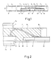
- Figure 1 shows a cross section through an information card according to the invention, which mainly consists of a card body 3, which is covered by an upper cover sheet 1 and a lower cover sheet 2.
- the card body 3 has a recess 14 for a carrier body 4.
- the carrier body 4 is provided with a punch 10 into which a semiconductor chip 5 is inserted such that its lower surface lies in one plane with the lower surface of the carrier body 4.
- the carrier body 4 carries both on its top and on its underside conductor tracks 11 and 12, which are connected to each other in a suitable manner and which lead to connection contact surfaces 13, which are accessible through openings in the lower cover film 2 of the information card in order to contact the in to enable the card contained semiconductor chips.
- the contact surfaces of the semiconductor chip 5 are through, for. B. with the help of an ultrasonic tape method attached wire connections 7 to the conductor tracks 11 on the top of the support body 4.
- the arc of the connecting wires 7 runs so flat that its highest point remains below the surface of the covering compound 9.
- the semiconductor chip 5 and the wire connections 7 on the top of the carrier body 4 are surrounded by an annular limiting body 8, the height of which is chosen so that the through its height and the thickness of the cover films 1 and 2 determined thickness of the entire card does not exceed the stated value of about 0.76 mm.
- the space formed within the annular boundary body 8 is filled with a covering compound 9 made of epoxy resin or silicone rubber.
- the upper cover sheet 1 is provided with a suitable window.
- the two cover foils 1 and 2 can be designed in two parts, the lower part 1 or 2 can carry an imprint etc., which is then protected by the upper part 1a or 2a.
- An information card constructed in this way is preferably produced as follows:
- a piece of film made of glass fiber-reinforced epoxy resin and having a thickness of 0.1 mm and serving as a carrier body 4 is first provided on both sides with conductor tracks 11, 12 and connection contact surfaces 13 made of gold.
- An opening 10 for the semiconductor chip 5 is then punched into this carrier body.
- the back of this carrier body 4 is glued with a self-adhesive film 15 and the semiconductor chip 5 is glued to this self-adhesive film 6 in the opening 15 in the carrier body 4.
- the wire connections 7 between the connection surfaces on the semiconductor chips 5 and the conductor tracks 11 on the upper side of the carrier body 4 are produced with an ultrasonic wire bonder which is usually used in the production of semiconductor components.
- a ring 8 likewise punched out of glass fiber reinforced epoxy resin and having a height of approximately 0.4 mm, is then glued onto the carrier body 4 in such a way that it surrounds the semiconductor chip 5 and the wire connections 7.
- the space surrounded by the annular boundary bodies via the semiconductor chip 5 and the wire connections 7 is then filled with a covering compound 9 made of epoxy resin filled with SiO 2 and this covering compound is then hardened by a heat treatment. Then the top of the limiting body 8 and the covering compound 9 is ground so far that the distance between the underside of the carrier body 4 and the top of the limiting body 8 is approximately 0.44 mm.
- the self-adhesive film 6, which previously carried the semiconductor chip 5, is peeled off and the unit comprising the carrier body 4 and the semiconductor chip 5 is inserted into the recess 14 of the card body 3 made of PVC (see FIG. 1) and both between an upper cover film 1 and a lower one Cover film 2, both also made of PVC, pressed together under pressure and elevated temperature and then cooled with the pressure maintained so that the finished information card has a standardized thickness of 0.76 mm.
- the lower cover film 2 is provided with openings over the contact surfaces 13 on the underside of the carrier body 4.
Landscapes
- Engineering & Computer Science (AREA)
- Computer Hardware Design (AREA)
- Microelectronics & Electronic Packaging (AREA)
- Physics & Mathematics (AREA)
- General Physics & Mathematics (AREA)
- Power Engineering (AREA)
- Condensed Matter Physics & Semiconductors (AREA)
- Theoretical Computer Science (AREA)
- Credit Cards Or The Like (AREA)
- Die Bonding (AREA)
- Structures Or Materials For Encapsulating Or Coating Semiconductor Devices Or Solid State Devices (AREA)
Applications Claiming Priority (2)
| Application Number | Priority Date | Filing Date | Title |
|---|---|---|---|
| DE3235650 | 1982-09-27 | ||
| DE19823235650 DE3235650A1 (de) | 1982-09-27 | 1982-09-27 | Informationskarte und verfahren zu ihrer herstellung |
Publications (3)
| Publication Number | Publication Date |
|---|---|
| EP0107061A2 EP0107061A2 (de) | 1984-05-02 |
| EP0107061A3 EP0107061A3 (en) | 1987-03-18 |
| EP0107061B1 true EP0107061B1 (de) | 1989-05-31 |
Family
ID=6174219
Family Applications (1)
| Application Number | Title | Priority Date | Filing Date |
|---|---|---|---|
| EP83109536A Expired EP0107061B1 (de) | 1982-09-27 | 1983-09-24 | Informationskarte und Verfahren zu ihrer Herstellung |
Country Status (5)
| Country | Link |
|---|---|
| US (1) | US4649418A (enExample) |
| EP (1) | EP0107061B1 (enExample) |
| JP (2) | JPS5990184A (enExample) |
| CA (1) | CA1203634A (enExample) |
| DE (2) | DE3235650A1 (enExample) |
Families Citing this family (79)
| Publication number | Priority date | Publication date | Assignee | Title |
|---|---|---|---|---|
| DE3248385A1 (de) * | 1982-12-28 | 1984-06-28 | GAO Gesellschaft für Automation und Organisation mbH, 8000 München | Ausweiskarte mit integriertem schaltkreis |
| JPS60589A (ja) * | 1983-06-16 | 1985-01-05 | Kyodo Printing Co Ltd | Icカ−ド |
| AU581196B2 (en) * | 1983-12-06 | 1989-02-16 | Mars, Incorporated | Tokens and token handling devices |
| JPS6121584A (ja) * | 1984-04-02 | 1986-01-30 | Toshiba Corp | Icカ−ド |
| US4727246A (en) * | 1984-08-31 | 1988-02-23 | Casio Computer Co., Ltd. | IC card |
| JPS6177992A (ja) * | 1984-09-25 | 1986-04-21 | Kyodo Printing Co Ltd | Icカ−ド |
| JPS6186885A (ja) * | 1984-10-04 | 1986-05-02 | Toshiba Corp | Icカ−ド |
| FR2580416B1 (fr) * | 1985-04-12 | 1987-06-05 | Radiotechnique Compelec | Procede et dispositif pour fabriquer une carte d'identification electronique |
| US4755661A (en) * | 1986-01-10 | 1988-07-05 | Ruebsam Herrn H | Connection of electronic components in a card |
| JPS62161595A (ja) * | 1986-01-13 | 1987-07-17 | 日立マクセル株式会社 | Icカ−ドの製造方法 |
| JP2502511B2 (ja) * | 1986-02-06 | 1996-05-29 | 日立マクセル株式会社 | 半導体装置の製造方法 |
| EP0246893A3 (en) * | 1986-05-21 | 1989-03-22 | Hitachi, Ltd. | Semiconductor device comprising an insulating wiring substrate and method of manufacturing it |
| JPS62290592A (ja) * | 1986-06-11 | 1987-12-17 | 大日本印刷株式会社 | カ−ド内蔵用icモジユ−ルの製造法 |
| JPS6314455A (ja) * | 1986-07-07 | 1988-01-21 | Hitachi Maxell Ltd | 半導体装置 |
| JPS63149191A (ja) * | 1986-12-15 | 1988-06-21 | 日立マクセル株式会社 | Icカ−ド |
| DE3723547C2 (de) * | 1987-07-16 | 1996-09-26 | Gao Ges Automation Org | Trägerelement zum Einbau in Ausweiskarten |
| US5304513A (en) * | 1987-07-16 | 1994-04-19 | Gao Gesellschaft Fur Automation Und Organisation Mbh | Method for manufacturing an encapsulated semiconductor package using an adhesive barrier frame |
| US4921160A (en) * | 1988-02-29 | 1990-05-01 | American Telephone And Telegraph Company | Personal data card and method of constructing the same |
| GB8901189D0 (en) * | 1989-01-19 | 1989-03-15 | Avery W & T Limited | Portable electronic token |
| US5258647A (en) * | 1989-07-03 | 1993-11-02 | General Electric Company | Electronic systems disposed in a high force environment |
| DE3924439A1 (de) * | 1989-07-24 | 1991-04-18 | Edgar Schneider | Traegerelement mit wenigstens einem integrierten schaltkreis, insbesondere zum einbau in chip-karten, sowie verfahren zur herstellung dieser traegerelemente |
| FR2662000A1 (fr) * | 1990-05-11 | 1991-11-15 | Philips Composants | Carte a microcircuit. |
| JP2560895B2 (ja) * | 1990-07-25 | 1996-12-04 | 三菱電機株式会社 | Icカードの製造方法およびicカード |
| EP0473260B1 (en) * | 1990-08-28 | 1995-12-27 | International Business Machines Corporation | Fabrication of semiconductor packages |
| JPH04164361A (ja) * | 1990-10-29 | 1992-06-10 | Nec Corp | 樹脂封止型半導体装置 |
| DE9100665U1 (de) * | 1991-01-21 | 1992-07-16 | TELBUS Gesellschaft für elektronische Kommunikations-Systeme mbH, 85391 Allershausen | Trägerelement für integrierte Halbleiter-Schaltkreise, insbesondere zum Einbau in Chip-Karten |
| GB2253591A (en) * | 1991-03-15 | 1992-09-16 | Gec Avery Ltd | Integrated circuit card |
| FR2677785A1 (fr) * | 1991-06-17 | 1992-12-18 | Philips Composants | Procede de fabrication d'une carte a microcircuit. |
| US5272596A (en) * | 1991-06-24 | 1993-12-21 | At&T Bell Laboratories | Personal data card fabricated from a polymer thick-film circuit |
| DE4122049A1 (de) * | 1991-07-03 | 1993-01-07 | Gao Ges Automation Org | Verfahren zum einbau eines traegerelements |
| FR2684235B1 (fr) * | 1991-11-25 | 1999-12-10 | Gemplus Card Int | Carte a circuit integre comprenant des moyens de protection du circuit integre. |
| US5350945A (en) * | 1991-12-18 | 1994-09-27 | Casio Computer Co., Ltd. | Coin-shaped integrated circuit memory device |
| US5523618A (en) * | 1992-05-25 | 1996-06-04 | Gay Freres Vente Et Exportation | Electronic integrated circuit label |
| TW258829B (enExample) * | 1994-01-28 | 1995-10-01 | Ibm | |
| JPH09501533A (ja) * | 1994-04-18 | 1997-02-10 | ガイ フレール バーント エ エクスポルタシオン ソシエテ アノニム | 物体用電子メモリ素子 |
| NL9400766A (nl) * | 1994-05-09 | 1995-12-01 | Euratec Bv | Werkwijze voor het inkapselen van een geintegreerde halfgeleiderschakeling. |
| JPH0831988A (ja) * | 1994-07-20 | 1996-02-02 | Nec Corp | テープキャリアパッケージの封止構造 |
| CA2176625C (en) * | 1995-05-19 | 2008-07-15 | Donald Harold Fergusen | Radio frequency identification tag |
| US6496382B1 (en) | 1995-05-19 | 2002-12-17 | Kasten Chase Applied Research Limited | Radio frequency identification tag |
| FR2735257B1 (fr) * | 1995-06-09 | 1997-08-29 | Solaic Sa | Carte laminee a circuit integre |
| JP2844558B2 (ja) * | 1995-06-29 | 1999-01-06 | 信越ポリマー株式会社 | チップ状半導体素子装着用の配線回路基板およびその製造方法 |
| US5633533A (en) * | 1995-07-26 | 1997-05-27 | International Business Machines Corporation | Electronic package with thermally conductive support member having a thin circuitized substrate and semiconductor device bonded thereto |
| US6013948A (en) | 1995-11-27 | 2000-01-11 | Micron Technology, Inc. | Stackable chip scale semiconductor package with mating contacts on opposed surfaces |
| US5674785A (en) * | 1995-11-27 | 1997-10-07 | Micron Technology, Inc. | Method of producing a single piece package for semiconductor die |
| US6861290B1 (en) * | 1995-12-19 | 2005-03-01 | Micron Technology, Inc. | Flip-chip adaptor package for bare die |
| DE19611237A1 (de) * | 1996-03-21 | 1997-09-25 | Siemens Ag | Multichipkarte |
| FR2748336A1 (fr) * | 1996-05-06 | 1997-11-07 | Solaic Sa | Carte a memoire a circuit integre enchasse dans le corps de carte |
| FR2749687B1 (fr) * | 1996-06-07 | 1998-07-17 | Solaic Sa | Carte a memoire et procede de fabrication d'une telle carte |
| US5811879A (en) * | 1996-06-26 | 1998-09-22 | Micron Technology, Inc. | Stacked leads-over-chip multi-chip module |
| US5773884A (en) * | 1996-06-27 | 1998-06-30 | International Business Machines Corporation | Electronic package with thermally conductive support member having a thin circuitized substrate and semiconductor device bonded thereto |
| DE19632813C2 (de) * | 1996-08-14 | 2000-11-02 | Siemens Ag | Verfahren zur Herstellung eines Chipkarten-Moduls, unter Verwendung dieses Verfahrens hergestellter Chipkarten-Modul und diesen Chipkarten-Modul enthaltende Kombi-Chipkarte |
| US6250192B1 (en) * | 1996-11-12 | 2001-06-26 | Micron Technology, Inc. | Method for sawing wafers employing multiple indexing techniques for multiple die dimensions |
| EP0919950B1 (en) * | 1997-06-23 | 2007-04-04 | Rohm Co., Ltd. | Module for ic card, ic card, and method for manufacturing module for ic card |
| SE518572C2 (sv) * | 1997-08-25 | 2002-10-22 | Ericsson Telefon Ab L M | Bärarelement för ett chips samt chipsmodul |
| US5962810A (en) * | 1997-09-09 | 1999-10-05 | Amkor Technology, Inc. | Integrated circuit package employing a transparent encapsulant |
| US5899705A (en) | 1997-11-20 | 1999-05-04 | Akram; Salman | Stacked leads-over chip multi-chip module |
| US6138349A (en) | 1997-12-18 | 2000-10-31 | Vlt Corporation | Protective coating for an electronic device |
| US6326696B1 (en) | 1998-02-04 | 2001-12-04 | International Business Machines Corporation | Electronic package with interconnected chips |
| EP0942392A3 (en) * | 1998-03-13 | 2000-10-18 | Kabushiki Kaisha Toshiba | Chip card |
| USRE43112E1 (en) | 1998-05-04 | 2012-01-17 | Round Rock Research, Llc | Stackable ball grid array package |
| US6040622A (en) * | 1998-06-11 | 2000-03-21 | Sandisk Corporation | Semiconductor package using terminals formed on a conductive layer of a circuit board |
| US6414391B1 (en) | 1998-06-30 | 2002-07-02 | Micron Technology, Inc. | Module assembly for stacked BGA packages with a common bus bar in the assembly |
| SG80077A1 (en) * | 1998-10-19 | 2001-04-17 | Sony Corp | Semiconductor integrated circuit card manufacturing method, and semiconductor integrated circuit card |
| TW368707B (en) * | 1998-10-27 | 1999-09-01 | Tech Field Co Ltd | Packaging method for semiconductor die and the product of the same |
| US6815251B1 (en) | 1999-02-01 | 2004-11-09 | Micron Technology, Inc. | High density modularity for IC's |
| JP4470242B2 (ja) * | 1999-04-23 | 2010-06-02 | ソニー株式会社 | 半導体メモリカード |
| US6624005B1 (en) | 2000-09-06 | 2003-09-23 | Amkor Technology, Inc. | Semiconductor memory cards and method of making same |
| DE10111028A1 (de) * | 2001-03-07 | 2002-09-19 | Infineon Technologies Ag | Chipkartenmodul |
| DE10208168C1 (de) * | 2002-02-26 | 2003-08-14 | Infineon Technologies Ag | Datenträgerkarte |
| US6653723B2 (en) * | 2002-03-09 | 2003-11-25 | Fujitsu Limited | System for providing an open-cavity low profile encapsulated semiconductor package |
| FR2838850B1 (fr) * | 2002-04-18 | 2005-08-05 | Framatome Connectors Int | Procede de conditionnement de microcircuits electroniques pour carte a puce et microcircuit electronique ainsi obtenu |
| JP3678212B2 (ja) * | 2002-05-20 | 2005-08-03 | ウシオ電機株式会社 | 超高圧水銀ランプ |
| US6924496B2 (en) * | 2002-05-31 | 2005-08-02 | Fujitsu Limited | Fingerprint sensor and interconnect |
| US6755700B2 (en) * | 2002-11-12 | 2004-06-29 | Modevation Enterprises Inc. | Reset speed control for watercraft |
| US7146029B2 (en) * | 2003-02-28 | 2006-12-05 | Fujitsu Limited | Chip carrier for fingerprint sensor |
| DE102009023854B4 (de) * | 2009-06-04 | 2023-11-09 | OSRAM Opto Semiconductors Gesellschaft mit beschränkter Haftung | Optoelektronisches Halbleiterbauelement |
| WO2011079741A1 (en) * | 2009-12-31 | 2011-07-07 | Huawei Technologies Co., Ltd. | A microwave unit and method therefore |
| USD983261S1 (en) | 2019-12-20 | 2023-04-11 | Capital One Services, Llc | Vented laminated card |
| US12124905B1 (en) * | 2021-12-17 | 2024-10-22 | Wells Fargo Bank, N.A. | Transaction instrument with features for destruction and disposal |
Family Cites Families (21)
| Publication number | Priority date | Publication date | Assignee | Title |
|---|---|---|---|---|
| US3637994A (en) * | 1970-10-19 | 1972-01-25 | Trw Inc | Active electrical card device |
| US3885304A (en) * | 1972-03-23 | 1975-05-27 | Bosch Gmbh Robert | Electric circuit arrangement and method of making the same |
| US4004133A (en) * | 1974-12-30 | 1977-01-18 | Rca Corporation | Credit card containing electronic circuit |
| JPS51130866A (en) * | 1975-05-08 | 1976-11-13 | Seiko Instr & Electronics | Method of mounting electronic timekeeper circuits |
| JPS51150068A (en) * | 1975-06-19 | 1976-12-23 | Citizen Watch Co Ltd | Electronic circuit block |
| JPS5242765A (en) * | 1975-09-30 | 1977-04-02 | Seiko Instr & Electronics Ltd | Electronic watch |
| FR2337381A1 (fr) * | 1975-12-31 | 1977-07-29 | Honeywell Bull Soc Ind | Carte portative pour systeme de traitement de signaux electriques et procede de fabrication de cette carte |
| US4222516A (en) * | 1975-12-31 | 1980-09-16 | Compagnie Internationale Pour L'informatique Cii-Honeywell Bull | Standardized information card |
| US4218701A (en) * | 1978-07-24 | 1980-08-19 | Citizen Watch Co., Ltd. | Package for an integrated circuit having a container with support bars |
| FR2439478A1 (fr) * | 1978-10-19 | 1980-05-16 | Cii Honeywell Bull | Boitier plat pour dispositifs a circuits integres |
| JPS5562591A (en) * | 1978-10-30 | 1980-05-12 | Fujitsu Ltd | Memory card |
| DE2920012C2 (de) * | 1979-05-17 | 1988-09-29 | GAO Gesellschaft für Automation und Organisation mbH, 8000 München | Ausweiskarte mit IC-Baustein und Verfahren zur Herstellung einer derartigen Ausweiskarte |
| FR2486685B1 (fr) * | 1980-07-09 | 1985-10-31 | Labo Electronique Physique | Carte de paiement electronique et procede de realisation |
| DE3051195C2 (de) * | 1980-08-05 | 1997-08-28 | Gao Ges Automation Org | Trägerelement zum Einbau in Ausweiskarten |
| DE3123198C2 (de) * | 1980-12-08 | 1993-10-07 | Gao Ges Automation Org | Trägerelemente für einen IC-Baustein |
| DE3047322A1 (de) * | 1980-12-16 | 1982-07-29 | Philips Patentverwaltung Gmbh, 2000 Hamburg | "datenverarbeitungsvorrichtung mit einem mobilen, elektronischen datentraeger" |
| DE3130213A1 (de) * | 1981-07-30 | 1983-02-17 | Siemens AG, 1000 Berlin und 8000 München | Verfahren zur herstellung einer tragbaren karte zur informationsverarbeitung |
| US4483067A (en) * | 1981-09-11 | 1984-11-20 | U.S. Philips Corporation | Method of manufacturing an identification card and an identification manufactured, for example, by this method |
| JPS5894132A (ja) * | 1981-11-28 | 1983-06-04 | Dainippon Printing Co Ltd | カ−ド |
| JPS58138057A (ja) * | 1982-02-12 | 1983-08-16 | Dainippon Printing Co Ltd | Icカ−ド |
| JPS5948985A (ja) * | 1982-09-13 | 1984-03-21 | 大日本印刷株式会社 | Icカ−ドの製造方法 |
-
1982
- 1982-09-27 DE DE19823235650 patent/DE3235650A1/de not_active Withdrawn
-
1983
- 1983-09-22 US US06/534,999 patent/US4649418A/en not_active Expired - Fee Related
- 1983-09-22 CA CA000437318A patent/CA1203634A/en not_active Expired
- 1983-09-24 EP EP83109536A patent/EP0107061B1/de not_active Expired
- 1983-09-24 DE DE8383109536T patent/DE3379988D1/de not_active Expired
- 1983-09-27 JP JP58177200A patent/JPS5990184A/ja active Pending
-
1991
- 1991-08-16 JP JP1991072506U patent/JPH0489382U/ja active Pending
Also Published As
| Publication number | Publication date |
|---|---|
| US4649418A (en) | 1987-03-10 |
| DE3379988D1 (en) | 1989-07-06 |
| EP0107061A2 (de) | 1984-05-02 |
| DE3235650A1 (de) | 1984-03-29 |
| EP0107061A3 (en) | 1987-03-18 |
| JPH0489382U (enExample) | 1992-08-04 |
| CA1203634A (en) | 1986-04-22 |
| JPS5990184A (ja) | 1984-05-24 |
Similar Documents
| Publication | Publication Date | Title |
|---|---|---|
| EP0107061B1 (de) | Informationskarte und Verfahren zu ihrer Herstellung | |
| EP0931343B1 (de) | Chipmodul insbesondere zur implantation in einen chipkartenkörper | |
| EP0919041B1 (de) | Verfahren zur herstellung eines chipkarten-moduls für eine kombi-chipkarte | |
| DE68921179T2 (de) | Elektronisches Modul mit einer integrierten Schaltung für ein kleines tragbares Objekt, z.B. eine Karte oder ein Schlüssel und Herstellungsverfahren für solche Module. | |
| DE69501361T2 (de) | Verfahren zur Einkapselung einer integrierten Schaltung | |
| DE3236567A1 (de) | Optischer koppler mit einem leiterrahmen sowie leiterrahmen dafuer | |
| EP0682321A2 (de) | Datenträger mit integriertem Schaltkreis | |
| DE69832104T2 (de) | Verbindung durch Aufbringen eines dem Relief entsprechenden viskosen Produktes | |
| EP1269410B1 (de) | Verfahren zur herstellung eines trägerbandes mit einer vielzahl von elektrischen einheiten, jeweils aufweisend einen chip und kontaktelemente | |
| DE3810899C2 (enExample) | ||
| DE4326816A1 (de) | Elektronisches Modul für Karten und Herstellung eines solchen Moduls | |
| EP1065624B1 (de) | Chipmodul zum Einbau in einen Chipkartenträger | |
| DE60005511T2 (de) | Laminierherstellungsverfahren einer kontaktlosen karte | |
| DE2101028C2 (de) | Verfahren zum Herstellen einer Mehrzahl von Halbleiterbauelementen | |
| EP0591668A1 (de) | Verfahren zur Montage von integrierten Halbleiterschaltkreisen | |
| DE19710656A1 (de) | Chipkarte | |
| DE10200569A1 (de) | Chipkarte und Herstellungsverfahren | |
| DE19610044C2 (de) | Kartenkörper und Verfahren zur Herstellung einer Chipkarte | |
| DE3619636A1 (de) | Gehaeuse fuer integrierte schaltkreise | |
| EP0183910A2 (de) | Verfahren zur Herstellung verformbarer Vielfach-Verbindungen für den elektrischen Anschluss mikroelektronischer Bauelemente und nach diesem Verfahren hergesttellte Vielfachverbindungen | |
| DE4321592A1 (de) | Halbleitervorrichtungen sowie Trägerteile und Leiterrahmen hierfür | |
| DE4423575A1 (de) | Datenträger mit einem Modul mit integriertem Schaltkreis | |
| DE69125313T2 (de) | Elektronisches Bauteil, das einen Leiterrahmen mit eingebautem Kondensator enthält | |
| EP1186037B1 (de) | Multichipmodul für die loc-montage sowie verfahren zu dessen herstellung. | |
| WO1999026287A1 (de) | Siliziumfolie als träger von halbleiterschaltungen als teil von karten |
Legal Events
| Date | Code | Title | Description |
|---|---|---|---|
| PUAI | Public reference made under article 153(3) epc to a published international application that has entered the european phase |
Free format text: ORIGINAL CODE: 0009012 |
|
| AK | Designated contracting states |
Designated state(s): CH DE FR GB IT LI |
|
| PUAL | Search report despatched |
Free format text: ORIGINAL CODE: 0009013 |
|
| AK | Designated contracting states |
Kind code of ref document: A3 Designated state(s): CH DE FR GB IT LI |
|
| 17P | Request for examination filed |
Effective date: 19870611 |
|
| RAP1 | Party data changed (applicant data changed or rights of an application transferred) |
Owner name: N.V. PHILIPS' GLOEILAMPENFABRIEKEN Owner name: PHILIPS PATENTVERWALTUNG GMBH |
|
| 17Q | First examination report despatched |
Effective date: 19880118 |
|
| GRAA | (expected) grant |
Free format text: ORIGINAL CODE: 0009210 |
|
| AK | Designated contracting states |
Kind code of ref document: B1 Designated state(s): CH DE FR GB IT LI |
|
| REF | Corresponds to: |
Ref document number: 3379988 Country of ref document: DE Date of ref document: 19890706 |
|
| ITF | It: translation for a ep patent filed | ||
| ET | Fr: translation filed | ||
| GBT | Gb: translation of ep patent filed (gb section 77(6)(a)/1977) | ||
| PLBI | Opposition filed |
Free format text: ORIGINAL CODE: 0009260 |
|
| 26 | Opposition filed |
Opponent name: GAO GESELLSCHAFT FUER AUTOMATION UND ORGANISATION Effective date: 19900223 |
|
| PGFP | Annual fee paid to national office [announced via postgrant information from national office to epo] |
Ref country code: FR Payment date: 19900920 Year of fee payment: 8 |
|
| PGFP | Annual fee paid to national office [announced via postgrant information from national office to epo] |
Ref country code: DE Payment date: 19901123 Year of fee payment: 8 |
|
| PGFP | Annual fee paid to national office [announced via postgrant information from national office to epo] |
Ref country code: CH Payment date: 19901217 Year of fee payment: 8 |
|
| REG | Reference to a national code |
Ref country code: CH Ref legal event code: PL |
|
| REG | Reference to a national code |
Ref country code: FR Ref legal event code: ST |
|
| PGFP | Annual fee paid to national office [announced via postgrant information from national office to epo] |
Ref country code: GB Payment date: 19920828 Year of fee payment: 10 |
|
| ITTA | It: last paid annual fee | ||
| RDAG | Patent revoked |
Free format text: ORIGINAL CODE: 0009271 |
|
| STAA | Information on the status of an ep patent application or granted ep patent |
Free format text: STATUS: PATENT REVOKED |
|
| 27W | Patent revoked |
Effective date: 19910316 |
|
| GBPR | Gb: patent revoked under art. 102 of the ep convention designating the uk as contracting state |
Free format text: 910316 |