EP0104988A1 - Delta-Sigma-Kodierer mit doppelter Integration und Anwendung dieses Kodierers bei einer PCM-Übertragungsstrecke und bei der Messung von Gleichstromspannungen - Google Patents
Delta-Sigma-Kodierer mit doppelter Integration und Anwendung dieses Kodierers bei einer PCM-Übertragungsstrecke und bei der Messung von Gleichstromspannungen Download PDFInfo
- Publication number
- EP0104988A1 EP0104988A1 EP83401807A EP83401807A EP0104988A1 EP 0104988 A1 EP0104988 A1 EP 0104988A1 EP 83401807 A EP83401807 A EP 83401807A EP 83401807 A EP83401807 A EP 83401807A EP 0104988 A1 EP0104988 A1 EP 0104988A1
- Authority
- EP
- European Patent Office
- Prior art keywords
- signal
- input
- output
- switches
- amplifier
- Prior art date
- Legal status (The legal status is an assumption and is not a legal conclusion. Google has not performed a legal analysis and makes no representation as to the accuracy of the status listed.)
- Granted
Links
Images


Classifications
-
- H—ELECTRICITY
- H04—ELECTRIC COMMUNICATION TECHNIQUE
- H04B—TRANSMISSION
- H04B14/00—Transmission systems not characterised by the medium used for transmission
- H04B14/02—Transmission systems not characterised by the medium used for transmission characterised by the use of pulse modulation
- H04B14/06—Transmission systems not characterised by the medium used for transmission characterised by the use of pulse modulation using differential modulation, e.g. delta modulation
- H04B14/062—Transmission systems not characterised by the medium used for transmission characterised by the use of pulse modulation using differential modulation, e.g. delta modulation using delta modulation or one-bit differential modulation [1DPCM]
-
- H—ELECTRICITY
- H03—ELECTRONIC CIRCUITRY
- H03M—CODING; DECODING; CODE CONVERSION IN GENERAL
- H03M3/00—Conversion of analogue values to or from differential modulation
- H03M3/30—Delta-sigma modulation
- H03M3/39—Structural details of delta-sigma modulators, e.g. incremental delta-sigma modulators
- H03M3/436—Structural details of delta-sigma modulators, e.g. incremental delta-sigma modulators characterised by the order of the loop filter, e.g. error feedback type
- H03M3/438—Structural details of delta-sigma modulators, e.g. incremental delta-sigma modulators characterised by the order of the loop filter, e.g. error feedback type the modulator having a higher order loop filter in the feedforward path
- H03M3/454—Structural details of delta-sigma modulators, e.g. incremental delta-sigma modulators characterised by the order of the loop filter, e.g. error feedback type the modulator having a higher order loop filter in the feedforward path with distributed feedback, i.e. with feedback paths from the quantiser output to more than one filter stage
-
- H—ELECTRICITY
- H03—ELECTRONIC CIRCUITRY
- H03M—CODING; DECODING; CODE CONVERSION IN GENERAL
- H03M3/00—Conversion of analogue values to or from differential modulation
- H03M3/30—Delta-sigma modulation
- H03M3/39—Structural details of delta-sigma modulators, e.g. incremental delta-sigma modulators
- H03M3/412—Structural details of delta-sigma modulators, e.g. incremental delta-sigma modulators characterised by the number of quantisers and their type and resolution
- H03M3/422—Structural details of delta-sigma modulators, e.g. incremental delta-sigma modulators characterised by the number of quantisers and their type and resolution having one quantiser only
- H03M3/43—Structural details of delta-sigma modulators, e.g. incremental delta-sigma modulators characterised by the number of quantisers and their type and resolution having one quantiser only the quantiser being a single bit one
Definitions
- the present invention relates to a digital-analog encoder, of Delta-Sigma type, with double integration.
- This invention applies to the coding of signals and, more particularly, to the transmission of signals over communication channels of the M IC type (Coded Impulse Modulation); it also applies to the measurement of direct voltages.
- the circuits integrated on substrate and in particular the digital signal processing circuits are more and more numerous and complex.
- the quality of the signal processing obtained thanks to these circuits, as well as the technological performances (size of the circuits, low dissipated power, reliability ...) allow to continuously consider new uses of these circuits in fields which, until then, were reserved for analog circuits.
- there is currently a difficult problem to solve which is that of the interface between the analog part and the digital part of a functional unit. If digital processing techniques have evolved very quickly, it is not the same for analog-digital interfaces.
- Noise spectrum shaping encoders make it possible to minimize the number of elements which must operate in linear mode and which perform the major part. processing in digital form.
- the advantage of these coders is that they make it possible to benefit as much as possible from the techniques for integrating digital circuits.
- the analog part can either be produced from discrete elements, or integrated on an analog circuit Annex, or even integrated directly on the digital processing circuit, if technology allows.
- Another advantage of this type of coders comes from the fact that when they use quantization on a single binary element, for conv digital version, they are very insensitive to transmission disturbances in a very noisy environment, such as an industrial environment for example.
- the principle of shaping the noise spectrum used in these encoders also makes them very efficient in measuring DC voltage at low flow rate.
- the delta-sigma type analog-digital encoders with double integration are specific encoders whose structure and operating principle derive directly from the structure and operation of encoders with noise spectrum shaping.
- delta-sigma coders as a sampler in an analog-M I C converter was proposed in the article "A single Channel PCM Codec" by JD EVERARD, IEEE, ICC 1978, Toronto June 1978.
- the sampling frequency is 2.048 MHz. This frequency does not make it possible to obtain the signal / noise ratio imposed by the standards, in particular at low levels. It has also been proposed (cf. "Improvements to delta sigma modulators when used for PCM encoding" by JD EVERARD in Electronics Letters, July 22, 1976, vol. L2, n ° 15 page 379) to increase the signal / noise ratio to low levels, by injecting an interference signal at a frequency such that it is filtered by the digital sub-sampling filter. This process increases the signal-to-noise ratio at low levels, but degrades it at high levels.
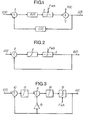
- FIG. 3 is a block diagram of a delta-sigma coder, dual integration, of known type, as described in French patent No. 2,462,062 cited above.
- the delta-sigma coder represented in this figure comprises a first adder 10 and a second adder 11.
- the first adder 10 receives on the one hand the input signal E (Z) and, on the other hand, the signal Q (Z ) output from the encoder.
- the output of this first adder is connected to the input of a first integrator 12.
- the output of the first integrator 12. is connected to an input of the second adder 11, which receives through a recursive feedback filter 13 of order two (multiplier by two), the output signal Q (Z) from the encoder.
- the output of the second adder 11 is connected to an input of a second integrator 14. Finally, the output of this second integrator. is connected to an input of a quantization circuit 15, controlled by a sampling signal having a sampling frequency Fech.
- the output of this sampling circuit constitutes the output of the dual integration delta-sigma encoder.
- the double integration delta sigma encoder represented in this figure comprises an operational amplifier 20, with, in its feedback path, a cell formed of two capacitors 21, 22 of capacitance C, connected in series, and of a resistor in parallel 23, of value R.
- the output of the operational amplifier is connected to two flip-flops in cascade 24 and 25 the outputs of these flip-flops are connected to the input of the operational amplifier 20 by resistors 26 and 27 of respective values R 'and 2R'.
- the value of the resistor 27 is twice that of the resistor 26 to make a binomial coder.
- the two scales 24 and 25, associated with resistances 26 and 27, carry out the transfer function
- the output of the second flip-flop is done on Q.
- Fech. represents the sampling frequency of the sampling signals applied to the inputs C of flip-flops 24 and 25, of type D, while + VREF and - VREF represent reference voltages applied to these flip-flops.
- This assembly is very sensitive to noise and the value of the components it uses makes it difficult to integrate.
- the object of the present invention is to remedy these drawbacks and in particular to produce a delta-sigma type coder, with double integration, little sensitive to noise, having easily integrated components.
- These aims are achieved by means of summers, integrators and filters (multiplier circuit) using switched capacitor circuits, in particular in the delta-sigma coder with double integration, as described in FIG. 3.
- the subject of the invention is a delta-sigma type coder, with double integration, comprising a first adder receiving, on a first input, a signal to be coded and receiving the signal coded on a second input, a first integrator receiving on an input an output signal of the first summator, a second summator receiving on a first input, the signal of an output of the first integrator, a second input of this second summator receiving a signal having an average amplitude proportional to the amplitude of the coded signal, a second integrator receiving on an input the output signal of the second summator, a quantizer circuit of which an input is connected to an output of the second integrator, and of which an input of control receives a signal for sampling the signal to be coded, an output of this quantizing circuit supplying the coded signal, characterized in that the first adder and the first integrator comprise a first operational amplifier, one output of which is connected to a negative input of this amplifier by an integration capacity, a positive input of this first amplifier being connected to
- each of the first non-inverting circuits comprises a first set of two switches connected in series between the reference ground and the negative input of the first amplifier and a second set of two switches connected in series between the reference ground and, respectively, for the first non-inverting circuits a line supplying the signal to be coded, and the output of the quantizing circuit, a switching capacity connecting in each of the first non-inverting circuits a point common to the switches of the first set with a point common to the switches of the second set, each of the second non-inverting circuits comprising a first set of two switches connected in series between the reference ground and the negative input of the second amplifier, and a second set of two switches connected in series between the reference mass and, respectively, for the second non-inverting circuits, the output of the first amplifier and the output of the quantizer circuit, a switching capacity connecting a point common to the switches of the first set to a point common to the switches of the second set.
- the encoder further comprises a clock circuit. supplying two trains of command pulses for opening and closing switches of non-reversing circuits, these pulses having a frequency equal to a sampling frequency of the signal to be coded, one of the switches of each set being open when the other is closed , and reciprocally.
- the quantizer circuit is a D type flip-flop, one input of which is connected to the output of the second amplifier, another control input of this flip-flop receiving the pulses from one of the trains, an output of this flip-flop providing the coded signal.
- the coder of the invention applies to a coding-decoding chain of a MIC type transmission channel, as well as to the measurement of DC voltages.
- FIGS. 1, 2, 3 and 4 have already been described to explain the operating principle of noise spectrum coders and delta-sigma type coders; they will not be described again.
- the dual-integration delta-sigma coder of the invention uses integrators and scmators with operational amplifiers and switched capacities.
- FIG. 5 schematically represents a circuit which makes it possible to simulate a resistance by switching a capacitance C between two voltage sources V 1 and V 2 , by means of two switches I 1 , I 2 , connected in series and receiving the voltages V 1 respectively , V 2 ; the common point of these switches is connected to one of the terminals of the capacitor C, the other terminal of this capacitor being connected to a reference ground M.
- This technique of Resistance simulation by capacitance switching is well known, in particular in MOS integrated circuits it is described in particular in the article "MOS SAMPLED DATA recursive filters using switched Capacitor Integrators" by HOSTICKA, BRODERSEN and GRAY. - IEEE Journal of Solid State Circuits, vol. SC-12, December 6, 1977.
- the resistance simulation technique by switched capacitors can be used to make an integrator-inverter circuit as shown in FIG. 6.
- This integrator comprises, in known manner, an operational amplifier 6 whose positive terminal is connected to the reference ground M the output S (P) of this amplifier, which also constitutes the output of the inverting integrator, is connected to the negative input of the operational amplifier via an integration capacitor C I.
- the integration resistance which is normally connected to the negative input of the operational amplifier is here simulated by a switched capacity circuit (described in FIG. 4), which receives the signal E (P) to be integrated.
- This circuit includes a capacitor Cm located between the reference ground M and the point common to the two switches I 1 , I 2 , controlled by the clock signals H l , H 2 .
- the essential advantage of this circuit is to be able to replace the integration product RC 1 , the elements of which are difficult to integrate precisely, while being compact, with a ratio of the capacities C m and C I which can be controlled so very precise, during an integrated circuit manufacturing process.
- FIG. 7 schematically represents a non-inverting integrator circuit, with switched capacities, which will, as will be seen in detail below, be used in the delta-sigma coder of the invention.
- This circuit is a variant of the circuit of FIG. 5 in which the load is reversed before injecting it towards the negative input of the operational amplifier, which itself is mounted as an inverter.
- the circuit comprises, as before, an operational amplifier 6, the positive terminal of which is connected to a reference ground M; the output S (P) of this amplifier, which also constitutes the output of the integrator circuit, is connected to the negative input of the amplifier, by an integration capacitor C I.
- the capacitance C m is associated with two sets of switches (I 1 , I 2 ), (I ' 1 , I' 2 ) whose openings and closings are controlled by clock signals H 1 , H 2 , at the Fech sampling frequency.
- the switches I 1 , I 2 are connected in series between the reference ground M and the negative input of the operational amplifier 6, their common point being connected to one of the terminals of the capacitor C m ; the switches I ' 1 , I' 2 are also connected in series.
- One of the terminals of the switch I ' 1 receives the input signal E (P) and one of the terminals of the switch I' 2 is connected to the reference ground M; the point common to the two switches is connected to another terminal of capacity C.
- This arrangement makes it possible to reverse the charge of the capacitor C m before injecting it at the input of the amplifier 6.
- the capacitor C m charges in the direction indicated by arrow 7, while when the switches I 2 , I ' 2 are closed, the capacity is charged in the direction of arrow 8 and the load is therefore inverted at the negative input of the operational amplifier mounted as an inverter.
- This circuit with switched capacitance is therefore non-inverting and makes it possible to simulate an integration resistance at the input of the operational amplifier 6 and has the main advantage of being insensitive to stray capacitances due to switches, precisely because it allows to reverse the charge of capacity C.
- the transfer function H (P) of this integrator-reverser is the same as that of the integrator-reverser of FIG. 6.
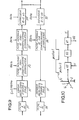
- FIG. 8 schematically represents a delta-sigma type coder, with double integration, in accordance with the invention.
- This coder comprises a first summing-integrator receiving on a first input 36 a signal E (P) to be coded and on a second input 37 the coded output signal S (P).
- the first adder and the first integrator comprise a first operational amplifier 30, an output 31 of which is connected to a negative input 32 of this amplifier, by an integration capacity CI 1 .
- a positive input 33 of this first amplifier is connected to a reference ground M.
- This first integrator and this first summator also include two first circuits
- This coder also comprises a second summing-integrator receiving on a first input 38 the output signal of the first integrator-summing and on a second input 39, a signal whose average amplitude is proportional to the amplitude of the coded output signal S (P).
- the second adder and the second integrator comprise a second operational amplifier 40 whose output 41 is connected, on the one hand, to a negative input 42 of this amplifier, by an integration capacity CI 2 , and on the other hand, to an input D of a quantizer circuit 43.
- This quantizer circuit consists of a flip-flop of type D.
- a positive input 44 of the second amplifier 40 is connected to the reference ground M.
- the second summator and the second integrator also include two second reversing circuits 45, 46 with switched capacities Cm 2 , C'm 2 . These two inverter circuits are connected in parallel on the inputs 42, 44 of the second amplifier 40. These circuits respectively receive, on inputs 38, 39, the output signal of the first amplifier 30 and a signal whose average amplitude is proportional to the amplitude of the coded signal.
- the coded signal S (P) is obtained on the complementary output Q of flip-flop D.
- This flip-flop also includes a control input to which H 2 signals of a clock circuit are applied, which will be described later in detail. Reference voltages + VREF and -VREF are applied to two other inputs of this flip-flop.
- Each of the first inverter circuits 34, 35 comprises a first set of two switches connected in series between the reference ground M and the negative input 32 of the first amplifier 30.
- the first set of two switches is shown in I 1 , I 2 , for the non-inverter circuit 34, while this first set of switches is shown in I 5 , 6, for the non-inverter circuit 35.
- Each of the first inverter circuits 34, 35 also includes a second set of switches connected in series between the reference ground M and, respectively, for these first two circuits, the input or line 36 providing the signal E (P) to code and the output Q of the quantizer circuit 43.
- the second sets of switches are represented respectively in I 3 , 1 4 and I 7 , I 8 .
- the second set of switches I 3 , I 4 is connected in series between the reference ground M and the input or line 36 supplying the signal E (P) to be coded.
- the second set of switches I 7 , I 8 is connected in series between the reference ground M and the output Q of the quantizer circuit 43.
- a switching capacity connects a common point to the switches of the first set at a common point to the switches of the second set. This is how the capacity Cm 1 connects the common point to switches II, I 2 , at a point common to switches I 3 , I 4 ; the capacity C'm l connects a point common to the switches I 5 , I 6 , to a point common to the switches I 7 , I 8 .
- Each of the second inverter circuits 45, 46 comprises a first set of two switches, connected in series between the reference ground M and the negative input 42 of the second amplifier 40; each of these circuits also comprises a second set of two switches, connected in series between the reference ground M and, respectively, for the two second inverter circuits, the output 31 of the first amplifier 30 and the output Q of the quantizer circuit 43.
- the first sets of two switches are represented respectively in I 9 , I 10 and I 15 , I 16 for the second circuits
- inverters 45, 46 the second sets of two switches are shown respectively in I 11 , I 12 and I 15 , and I 16 , for the second inverter circuits 45, 46.
- a switching capacity connects a common point to the switches of the first play at a point common to the switches of the second set. This is how the capacity Cm 2 connects a point common to the switches I 9 , I 10 , to a point common to the switches I 11 , I 12, and that the capacity C ' m 2 connects a point common to switches I 13 , I 14 , to a point common to switches I 15 , I 16 .
- the encoder also includes a clock circuit 47 supplying two trains of pulses H 1 , H 2 , for controlling the opening and closing of the switches of each of the reversing circuits 35, 36, 45, 46.
- These pulses have been described above, in Figures 5, 6, 7; the Pulse rate 8 2 of one of these trains of pulses are also applied to a flip-flop the control input 43.
- these pulses have a frequency equal to the sampling frequency of the signal to be coded and they act so that one of the switches in each set is open when the other is closed, and vice versa.
- inverter is connected to point A shown in this figure.
- the average amplitude of the signal applied to the negative input 42 of the second operational amplifier 40 is proportional to the average amplitude of the coded signal F (P) output from the coder. This proportionality is obtained by a predetermined choice of the values of the capacities Cm 2 , C'm 2 .
- This encoder does not require any device to ensure its statibility or adjustment. It is in particular very easily integrated by a manufacturing process using a MOS technique.
- the transfer function becomes:
- Hp (Z) does not modify the signal-to-noise ratio of the encoder in a signal band B, but brings about a slight modification of the spectrum of the input signal, but it must be taken into account that the sampling frequency is very large compared to the maximum frequency of the signal to be coded.
- the signal limited to a 300-3400 Hz band is sampled at the frequency of 2048 kHz and the variation in attenuation provided by Hp (Z) is less than 0.02 decibels.
- the quantization operation is carried out by a simple D type flip-flop.
- This type of circuit is completely insensitive to the offset or offset of the operational amplifier. Indeed, this offset voltage can be considered as part of the noise brought about by the quantization operation and therefore, therefore, affected by the filtering function H (Z) which has an infinite theoretical attenuation at frequency 0.
- the coder of the invention can be applied to a coding-decoding chain of a MIC type transmission channel.
- This chain is represented in FIG. 9 and it is described in the French patent No. 2,462,062 cited above.
- the second order delta-sigma coder represented in this chain is in fact the coder of the invention, which has been described in FIG. 8.
- the chain includes an analog-MIC encoder and an analog MIC decoder per single transmission channel.
- the MIC decoder comprises an expander 55, 8eb - 12eb, operating at 8 kHz, a digital filter 56 oversampling interpolator, operating at 32 kHz, a delta-sigma decoder 57 of order 2 with double digital integration, conforming to the invention, operating at 2.048 MHz, and a Resistance-Capacity filter 58.
- the encoder of the invention also applies to the measurement of direct voltages.
- the encoder provides infinite attenuation on the quantization noise at zero frequency. It is therefore possible to carry out measurements of very fine continuous components with inexpensive equipment.
- FIG. 12 shows an exemplary embodiment of a continuous analog-digital converter using an encoder 63, according to the invention.
- the digital filtering is reduced to its simplest expression, that is to say a simple accumulation of data in an accumulator 60.
- the output signal from the encoder 63 is sampled at the frequency F / n, F being the frequency of arrival of the samples in the accumulator 60.
- I c is a control signal of the switch I, and H of the control clock signals of the unit 61 and of the delta-sigma encoder 63. If Tm designates the period of the signals Ic, the frequency F H of the signals H must be much greater than .
- the results of the measurements are obtained on the output 62 of the unit 61.
Landscapes
- Engineering & Computer Science (AREA)
- Theoretical Computer Science (AREA)
- Computer Networks & Wireless Communication (AREA)
- Signal Processing (AREA)
- Compression, Expansion, Code Conversion, And Decoders (AREA)
Applications Claiming Priority (2)
| Application Number | Priority Date | Filing Date | Title |
|---|---|---|---|
| FR8215857 | 1982-09-21 | ||
| FR8215857A FR2533382B1 (fr) | 1982-09-21 | 1982-09-21 | Codeur de type delta-sigma, a double integration et applications de ce codeur a une voie de transmission de type mic et a la mesure de tensions continues |
Publications (2)
| Publication Number | Publication Date |
|---|---|
| EP0104988A1 true EP0104988A1 (de) | 1984-04-04 |
| EP0104988B1 EP0104988B1 (de) | 1987-04-08 |
Family
ID=9277600
Family Applications (1)
| Application Number | Title | Priority Date | Filing Date |
|---|---|---|---|
| EP83401807A Expired EP0104988B1 (de) | 1982-09-21 | 1983-09-15 | Delta-Sigma-Kodierer mit doppelter Integration und Anwendung dieses Kodierers bei einer PCM-Übertragungsstrecke und bei der Messung von Gleichstromspannungen |
Country Status (5)
| Country | Link |
|---|---|
| US (1) | US4588981A (de) |
| EP (1) | EP0104988B1 (de) |
| CA (1) | CA1224877A (de) |
| DE (1) | DE3370916D1 (de) |
| FR (1) | FR2533382B1 (de) |
Cited By (5)
| Publication number | Priority date | Publication date | Assignee | Title |
|---|---|---|---|---|
| EP0084353A2 (de) * | 1982-01-20 | 1983-07-27 | Alcatel N.V. | Delta-Sigma Modulator mit geschalteter Kondensatorrealisierung |
| EP0232763A1 (de) * | 1986-02-04 | 1987-08-19 | Siemens Aktiengesellschaft | Elektronischer Elektrizitätszähler |
| EP0396786A1 (de) * | 1989-05-08 | 1990-11-14 | Siemens Aktiengesellschaft | Integrierbarer Sigma-Delta-Modulator in Switched-Capacitor-Technik |
| EP0615344A1 (de) * | 1993-03-11 | 1994-09-14 | France Telecom | Verbesserter Kodierer zur Rauschformung, insbesondere Sigma/Delta-Kodierer |
| WO1996018242A1 (en) * | 1994-12-09 | 1996-06-13 | Advanced Micro Devices, Inc. | Sigma-delta modulator with reduced delay from input to output |
Families Citing this family (35)
| Publication number | Priority date | Publication date | Assignee | Title |
|---|---|---|---|---|
| US4704600A (en) * | 1985-02-04 | 1987-11-03 | Nippon Telegraph And Telephone Corporation | Oversampling converter |
| US4796004A (en) * | 1986-02-14 | 1989-01-03 | General Instrument Corp. | Integrated analog-to-digital converter |
| US4937577A (en) * | 1986-02-14 | 1990-06-26 | Microchip Technology Inc. | Integrated analog-to-digital converter |
| JPH0797749B2 (ja) * | 1986-05-16 | 1995-10-18 | 沖電気工業株式会社 | アナログ・デイジタル変換器のデルタ・シグマ変調回路 |
| JPS63211987A (ja) * | 1987-02-27 | 1988-09-05 | Sony Corp | 予測符号化装置 |
| US4866442A (en) * | 1987-06-01 | 1989-09-12 | Steim Joseph M | Analog to digital converter employing delta-sigma modulation |
| US4876542A (en) * | 1988-01-25 | 1989-10-24 | Motorola, Inc. | Multiple output oversampling A/D converter with each output containing data and noise |
| JPH01204528A (ja) * | 1988-02-10 | 1989-08-17 | Fujitsu Ltd | A/d変換器 |
| JPH01233921A (ja) * | 1988-03-15 | 1989-09-19 | Toshiba Corp | △−σ変調器を用いたa/d変換回路 |
| JP2650711B2 (ja) * | 1988-03-25 | 1997-09-03 | 株式会社日立製作所 | オーバーサンプリングa/d変換器 |
| US4876543A (en) * | 1988-05-31 | 1989-10-24 | Motorola, Inc. | Multi-rate cascaded noise shaping modulator |
| US5150324A (en) * | 1988-06-09 | 1992-09-22 | Asahi Kasei Microsystems Co. Ltd. | Analog arithmetic circuit that can perform multiplication division expansion and compression by using delta sigma modulator |
| GB8818703D0 (en) * | 1988-08-05 | 1988-09-07 | Gen Electric Co Plc | Delta sigma modulator arrangements |
| US4918454A (en) * | 1988-10-13 | 1990-04-17 | Crystal Semiconductor Corporation | Compensated capacitors for switched capacitor input of an analog-to-digital converter |
| US5055846A (en) * | 1988-10-13 | 1991-10-08 | Crystal Semiconductor Corporation | Method for tone avoidance in delta-sigma converters |
| US5001725A (en) * | 1989-05-19 | 1991-03-19 | Teknekron Communications Systems, Inc. | Differential switched-capacitor sigma-delta modulator |
| US4951052A (en) * | 1989-07-10 | 1990-08-21 | General Electric Company | Correction of systematic error in an oversampled analog-to-digital converter |
| JPH07105724B2 (ja) * | 1989-07-14 | 1995-11-13 | ヤマハ株式会社 | ディジタル・アナログ変換回路 |
| US5079550A (en) * | 1989-10-27 | 1992-01-07 | Crystal Semiconductor Corporation | Combining continuous time and discrete time signal processing in a delta-sigma modulator |
| JP3011424B2 (ja) * | 1990-01-24 | 2000-02-21 | 株式会社東芝 | A/d変換器 |
| US5055843A (en) * | 1990-01-31 | 1991-10-08 | Analog Devices, Inc. | Sigma delta modulator with distributed prefiltering and feedback |
| ATE132675T1 (de) * | 1990-11-27 | 1996-01-15 | Gordon M Jacobs | Digitaler datenumsetzer |
| EP0495328B1 (de) * | 1991-01-15 | 1996-07-17 | International Business Machines Corporation | Sigma-Delta Wandler |
| US5159341A (en) * | 1991-03-12 | 1992-10-27 | Analog Devices, Inc. | Two phase sampling for a delta sigma modulator |
| US6037887A (en) * | 1996-03-06 | 2000-03-14 | Burr-Brown Corporation | Programmable gain for delta sigma analog-to-digital converter |
| US6816100B1 (en) | 1999-03-12 | 2004-11-09 | The Regents Of The University Of California | Analog-to-digital converters with common-mode rejection dynamic element matching, including as used in delta-sigma modulators |
| US6204787B1 (en) | 1999-03-31 | 2001-03-20 | Cirrus Logic, Inc. | Circuits and methods for gain ranging in an analog modulator and systems using the same |
| WO2000065723A1 (en) * | 1999-04-21 | 2000-11-02 | Koninklijke Philips Electronics N.V. | Sigma-delta analog-to-digital converter |
| US6473018B2 (en) * | 2000-04-13 | 2002-10-29 | Matsushita Electric Industrial Co., Ltd. | Delta sigma analog-to-digital converter |
| DE10036722C1 (de) * | 2000-07-27 | 2002-02-28 | Infineon Technologies Ag | Frequenzverdopplungsschaltung |
| TWI307213B (en) * | 2005-08-02 | 2009-03-01 | Realtek Semiconductor Corp | Reference voltage generating circuit |
| TWI349489B (en) * | 2006-09-07 | 2011-09-21 | Realtek Semiconductor Corp | Image processing device and method |
| JP4924370B2 (ja) * | 2007-01-26 | 2012-04-25 | パナソニック株式会社 | Σδ型ad変換器およびそれを用いた角速度センサ |
| JP6293516B2 (ja) * | 2014-02-28 | 2018-03-14 | ローム株式会社 | 2重積分型a/d変換器 |
| KR102224924B1 (ko) | 2014-11-24 | 2021-03-08 | 삼성전자주식회사 | 차동 출력을 갖는 델타-시그마 모듈레이터 |
Citations (1)
| Publication number | Priority date | Publication date | Assignee | Title |
|---|---|---|---|---|
| FR2462062A1 (fr) * | 1979-07-20 | 1981-02-06 | Petit Jean P | Codeur delta sigma a double integration analogique et codeur delta sigma a double integration numerique |
Family Cites Families (2)
| Publication number | Priority date | Publication date | Assignee | Title |
|---|---|---|---|---|
| JPS5625827A (en) * | 1979-08-10 | 1981-03-12 | Nec Corp | Coding unit |
| US4439756A (en) * | 1982-01-20 | 1984-03-27 | International Telephone And Telegraph Corporation | Delta-Sigma modulator with switch capacitor implementation |
-
1982
- 1982-09-21 FR FR8215857A patent/FR2533382B1/fr not_active Expired
-
1983
- 1983-09-15 DE DE8383401807T patent/DE3370916D1/de not_active Expired
- 1983-09-15 EP EP83401807A patent/EP0104988B1/de not_active Expired
- 1983-09-20 US US06/534,096 patent/US4588981A/en not_active Expired - Lifetime
- 1983-09-21 CA CA000437214A patent/CA1224877A/en not_active Expired
Patent Citations (1)
| Publication number | Priority date | Publication date | Assignee | Title |
|---|---|---|---|---|
| FR2462062A1 (fr) * | 1979-07-20 | 1981-02-06 | Petit Jean P | Codeur delta sigma a double integration analogique et codeur delta sigma a double integration numerique |
Non-Patent Citations (4)
| Title |
|---|
| IEEE JOURNAL OF SOLID-STATE CIRCUITS * |
| IEEE JOURNAL OF SOLID-STATE CIRCUITS, vol. SC-12, no. 6, décembre 1977, New York (US) * |
| PATENT ABSTRACTS OF JAPAN, vol. 5, no. 78 (E-58) (750), 22 mai 1981 * |
| REVIEW OF THE ELECTRICAL COMMUNICATION LABORATORIES, vol. 29, nos. 5-6, mai-juin 1981, Tokyo (JP) * |
Cited By (9)
| Publication number | Priority date | Publication date | Assignee | Title |
|---|---|---|---|---|
| EP0084353A2 (de) * | 1982-01-20 | 1983-07-27 | Alcatel N.V. | Delta-Sigma Modulator mit geschalteter Kondensatorrealisierung |
| EP0084353A3 (en) * | 1982-01-20 | 1985-08-14 | International Standard Electric Corporation | Delta-sigma modulator with switched capacitor implementation |
| EP0232763A1 (de) * | 1986-02-04 | 1987-08-19 | Siemens Aktiengesellschaft | Elektronischer Elektrizitätszähler |
| EP0396786A1 (de) * | 1989-05-08 | 1990-11-14 | Siemens Aktiengesellschaft | Integrierbarer Sigma-Delta-Modulator in Switched-Capacitor-Technik |
| US4999634A (en) * | 1989-05-08 | 1991-03-12 | Siemens Aktiengesellschaft | Integratable switched-capacitor sigma-delta modulator |
| EP0615344A1 (de) * | 1993-03-11 | 1994-09-14 | France Telecom | Verbesserter Kodierer zur Rauschformung, insbesondere Sigma/Delta-Kodierer |
| FR2702611A1 (fr) * | 1993-03-11 | 1994-09-16 | Senn Patrice | Codeur perfectionné à mise en forme du spectre de bruit, en particulier de type delta-sigma. |
| WO1996018242A1 (en) * | 1994-12-09 | 1996-06-13 | Advanced Micro Devices, Inc. | Sigma-delta modulator with reduced delay from input to output |
| US5648779A (en) * | 1994-12-09 | 1997-07-15 | Advanced Micro Devices, Inc. | Sigma-delta modulator having reduced delay from input to output |
Also Published As
| Publication number | Publication date |
|---|---|
| CA1224877A (en) | 1987-07-28 |
| US4588981A (en) | 1986-05-13 |
| DE3370916D1 (en) | 1987-05-14 |
| FR2533382B1 (fr) | 1988-01-22 |
| EP0104988B1 (de) | 1987-04-08 |
| FR2533382A1 (fr) | 1984-03-23 |
Similar Documents
| Publication | Publication Date | Title |
|---|---|---|
| EP0104988B1 (de) | Delta-Sigma-Kodierer mit doppelter Integration und Anwendung dieses Kodierers bei einer PCM-Übertragungsstrecke und bei der Messung von Gleichstromspannungen | |
| EP0559732B1 (de) | Digitaler datenumsetzer | |
| Fujimori et al. | A 1.5 V, 4.1 mW dual-channel audio delta-sigma D/A converter | |
| US6111531A (en) | Parallel architecture for a bandpass sigma-delta modulator | |
| FR2555377A1 (fr) | Circuit electronique utilisable dans les dispositifs a circuit integre contenant des filtres a condensateurs commutes | |
| FR2487142A1 (fr) | Circuit et procede de conversion a/n ou n/a de signaux bipolaires utilisant une unique tension de reference | |
| EP1646147A1 (de) | Analoges Filter für zeitdiskrete Signale aus passiven Bauelementen | |
| FR2619973A1 (fr) | Dispositif de filtre echantillonne a capacites commutees | |
| FR2462062A1 (fr) | Codeur delta sigma a double integration analogique et codeur delta sigma a double integration numerique | |
| FR2489627A1 (fr) | Codeur-decodeur | |
| EP0022695B1 (de) | Geschaltete Filtereinheit | |
| FR2551279A1 (fr) | Generateur d'onde sinusoidale, dont la frequence est asservie a un signal binaire, notamment pour modem | |
| WO2016131990A1 (fr) | Convertisseur sigma-delta a haute linearite | |
| EP3276833A1 (de) | Sigma-delta-wandler mit hoher linearität | |
| FR3011701A1 (fr) | Dispositif de quantification en temps continu, recepteur de signaux radiofrequence comprenant un tel dispositif et procede de quantification en temps continu | |
| EP0084474B1 (de) | Hochpassfilter erster Ordnung und Anwendung in der Telefonie | |
| EP0620641B1 (de) | Signalverarbeitungsanordnung mit mehreren verschiedenen Filtern, insbesondere für audiofrequente Codierung von Stimmensignalen | |
| WO2004001973A1 (fr) | Boucle a verrouillage de retard | |
| FR2809247A1 (fr) | Convertisseur analogique-numerique pipeline avec mise en forme de bruit | |
| FR2797725A1 (fr) | Procede et dispositif de conversion d'un signal analogique en un signal numerique avec controle automatique de gain | |
| Kim et al. | An area-efficient sigma-delta DAC with a current-mode semi-digital IFIR reconstruction filter | |
| YUKAWA et al. | Reprinted from ICASSP—IEEE INTERNATIONAL CONFERENCE ON ACOUSTICS, SPEECH, AND SIGNAL PROCESSING, March 26-29, 1985 AN OVERSAMPLING A-TO-D CONVERTER STRUCTURE FOR VLSI DIGITAL CODEC'S | |
| JP2003258644A (ja) | デルタ・シグマ変調器 | |
| WO2018115066A1 (fr) | Encodeur numérique pour signaux modulés, et dispositif de génération d'un signal analogique associé | |
| EP4155835A1 (de) | Digitaler zeitumwandler und phasenregelschleife |
Legal Events
| Date | Code | Title | Description |
|---|---|---|---|
| PUAI | Public reference made under article 153(3) epc to a published international application that has entered the european phase |
Free format text: ORIGINAL CODE: 0009012 |
|
| AK | Designated contracting states |
Designated state(s): DE GB IT |
|
| 17P | Request for examination filed |
Effective date: 19840908 |
|
| GRAA | (expected) grant |
Free format text: ORIGINAL CODE: 0009210 |
|
| AK | Designated contracting states |
Kind code of ref document: B1 Designated state(s): DE GB IT |
|
| REF | Corresponds to: |
Ref document number: 3370916 Country of ref document: DE Date of ref document: 19870514 |
|
| ITF | It: translation for a ep patent filed |
Owner name: JACOBACCI & PERANI S.P.A. |
|
| PLBE | No opposition filed within time limit |
Free format text: ORIGINAL CODE: 0009261 |
|
| STAA | Information on the status of an ep patent application or granted ep patent |
Free format text: STATUS: NO OPPOSITION FILED WITHIN TIME LIMIT |
|
| 26N | No opposition filed | ||
| ITTA | It: last paid annual fee | ||
| PGFP | Annual fee paid to national office [announced via postgrant information from national office to epo] |
Ref country code: DE Payment date: 20000830 Year of fee payment: 18 |
|
| PGFP | Annual fee paid to national office [announced via postgrant information from national office to epo] |
Ref country code: GB Payment date: 20000831 Year of fee payment: 18 |
|
| PG25 | Lapsed in a contracting state [announced via postgrant information from national office to epo] |
Ref country code: GB Free format text: LAPSE BECAUSE OF NON-PAYMENT OF DUE FEES Effective date: 20010915 |
|
| REG | Reference to a national code |
Ref country code: GB Ref legal event code: IF02 |
|
| PG25 | Lapsed in a contracting state [announced via postgrant information from national office to epo] |
Ref country code: DE Free format text: LAPSE BECAUSE OF NON-PAYMENT OF DUE FEES Effective date: 20020501 |
|
| GBPC | Gb: european patent ceased through non-payment of renewal fee |
Effective date: 20010915 |