EP0097724A1 - Procédé et dispositif de balayage - Google Patents
Procédé et dispositif de balayage Download PDFInfo
- Publication number
- EP0097724A1 EP0097724A1 EP82104843A EP82104843A EP0097724A1 EP 0097724 A1 EP0097724 A1 EP 0097724A1 EP 82104843 A EP82104843 A EP 82104843A EP 82104843 A EP82104843 A EP 82104843A EP 0097724 A1 EP0097724 A1 EP 0097724A1
- Authority
- EP
- European Patent Office
- Prior art keywords
- scanning
- light
- signal
- detection signal
- image signal
- Prior art date
- Legal status (The legal status is an assumption and is not a legal conclusion. Google has not performed a legal analysis and makes no representation as to the accuracy of the status listed.)
- Granted
Links
Images


Classifications
-
- H—ELECTRICITY
- H04—ELECTRIC COMMUNICATION TECHNIQUE
- H04N—PICTORIAL COMMUNICATION, e.g. TELEVISION
- H04N1/00—Scanning, transmission or reproduction of documents or the like, e.g. facsimile transmission; Details thereof
- H04N1/38—Circuits or arrangements for blanking or otherwise eliminating unwanted parts of pictures
-
- H—ELECTRICITY
- H04—ELECTRIC COMMUNICATION TECHNIQUE
- H04N—PICTORIAL COMMUNICATION, e.g. TELEVISION
- H04N1/00—Scanning, transmission or reproduction of documents or the like, e.g. facsimile transmission; Details thereof
- H04N1/024—Details of scanning heads ; Means for illuminating the original
- H04N1/028—Details of scanning heads ; Means for illuminating the original for picture information pick-up
- H04N1/0281—Details of scanning heads ; Means for illuminating the original for picture information pick-up with means for collecting light from a line or an area of the original and for guiding it to only one or a relatively low number of picture element detectors
-
- H—ELECTRICITY
- H04—ELECTRIC COMMUNICATION TECHNIQUE
- H04N—PICTORIAL COMMUNICATION, e.g. TELEVISION
- H04N1/00—Scanning, transmission or reproduction of documents or the like, e.g. facsimile transmission; Details thereof
- H04N1/40—Picture signal circuits
- H04N1/409—Edge or detail enhancement; Noise or error suppression
- H04N1/4097—Removing errors due external factors, e.g. dust, scratches
Definitions
- the invention relates to a method for optoelectronic scanning of documents which are arranged on a translucent document carrier, and a scanning device for flatbed or drum scanning devices.
- a light beam scans the original to be reproduced pixel by line and line by line.
- the scanning light coming from the original falls on an optoelectronic scanning element and is converted there into an image signal.
- the image signal is transmitted via a transmission channel to a facsimile recording device in which the reproduction of the original is recorded.
- the assembled templates are a multitude of Individual templates for writing and images that have been assembled on a template carrier to form a complete page.
- the individual templates can be either supervisory templates or see-through templates, and the adhesive assemblies are scanned accordingly in supervision or in review.
- the scanner should be applicable to both flatbed and drum scanners.
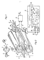
- FIG. 1 shows an advantageous exemplary embodiment of a scanning device for, in particular, adhesive mounting in a flatbed scanning device.
- Adhesive assembly 2 is individual templates 3 and 4 for writing and images, which have been assembled, for example with the help of hard wax, on a translucent template carrier 5 to form an entire page.
- the original carrier 5 can be a transparent film with a high transmittance, but also a thin paper with a relatively low transmittance.
- the individual templates 3 and 4 can either be supervisory templates or see-through templates.
- the axis of rotation 9 of the multi-surface rotating mirror 8 is aligned perpendicular to the optical axis of the light beam 7.
- a motor 10 drives the multi-surface rotating mirror 8 at a constant angular velocity in the direction of an arrow 11.
- the rotation of the multi-surface rotating mirror 8 turns the light emitted by the light source 6 beam 7 reflected from the individual mirror surfaces and continuously deflected by a lens 12 in the line direction 13 via the adhesive assembly 2.
- the scanning table 1 executes a step-by-step or continuous feed movement perpendicular to the line direction 13, as a result of which the adhesive assembly 2 is scanned point by point in adjacent lines.
- a first optoelectronic scanner 14 is arranged on the side of the scanning table 1 facing the light source 6 and a second optoelectronic scanner 15 is arranged on the opposite side.
- the first scanner 14 receives the scanning light reflected by the adhesive assembly 2 and generates a first scanning signal on a line 16, the second scanner 15 receives the transmitted scanning light and generates a second scanning signal on a line 17.
- the first and second scanning signals arrive via lines 16 and 17 in a compensation circuit 18 for amplitude errors in the image signal due to mounting or shadow edges and due to scratches.
- the compensation circuit 18 generates the corrected image signal U * for transmission to a facsimile recorder, not shown.
- the scanners 14 and 15 can be photodiode strips which extend over the line length, but also discrete photodiodes or photomultipliers which are carried along with the light beam in the line direction.
- the scanners 14 and 15 are advantageously designed as stationary light-receiving devices, for example in the form of hollow cylinders with slot-shaped openings aligned in the row direction.
- the light receiving device 14 of the upper scanner 14 has a light entry opening 19 for the scanning beam 7 'and a light passage opening 20 facing the scanning table 1 for the scanning beam 7' and the scanning light reflected from the original.
- the light-receiving device 15 ′ of the lower scanner 15 has only one light entry opening 21 facing the scanning table 1 for the scanning light that is let through by the adhesive assembly 2.
- Both light receiving devices 14 'and 15' also have light receiving surfaces 22 and 23, which are formed by those surfaces of optical cross-section transducers 24 and 25 which have the greatest extension.
- the optical cross-sectional transducers 24 and 25 are made up of a large number of optical fibers.
- the surfaces 26 and 27 of the optical cross-sectional transducers 24 and 25 with the smaller dimensions are connected to optoelectronic transducers 28 and 29, e.g. B. connected to photomultipliers, which generate the scanning signals on lines 16 and 17.
- the inner surfaces of the light-absorbing devices 14 'and 15' opposite the light-absorbing surfaces 22 and 23 are designed as diffuse reflectors 30 and 31, in each case in the region which depends on the opening angle of the light guide fibers is limited, from which the cross-sectional transducers 24 and 25 consist.
- the remaining inner surfaces of the light receiving devices 14 'and 15' are designed as mirrors 32 and 33. Alternatively, the entire inner surfaces of the light receiving devices 14 'and 15' can be diffusely reflective.
- the shape and spacing of the reflectors 30 and 31 are selected such that as large as possible a large proportion of the light diffusely reflected by them falls on the light-receiving surfaces 22 and 23 within the opening angle.
- the diffuse light coming from the reflectors 30 and 31, which does not directly hit the light receiving surfaces 22 and 23, is guided back to the reflectors 30 and 31 almost without loss by the mirrors 32 and 33 and is again diffusely reflected in the direction of the light receiving surfaces 22 and 23.
- Light receiving surface 22 and passage opening 20 on the one hand and light receiving surface 23 and light entry opening 21 on the other hand lie in such a way that no scanning light coming from the adhesive assembly 2 reaches the light receiving surfaces 22 or 23 directly, but diffusely reflects at least once on the reflectors 30 and 31 becomes.
- the light entry opening 19 of the light receiving device 14 ' is expediently chosen to be so large that the unmodulated scanning light reflected by a glossy original surface emerges directly from the light entry opening 19 and remains unconsidered.
- the light-receiving Devices 14 'and 15' thus have a high degree of efficiency, so that the light source 6 generating the scanning light beam 7 can have a lower output.
- the full opening angle of the optical fibers is used and the disruptive influence of scratches and shadow edges in the adhesive assembly is already reduced. Since the scattered light emanating from the reflectors 30 and 31 also spreads in the longitudinal extent of the light receiving surfaces 22 and 23, a large number of optical fibers are involved in the light transport to the optoelectronic transducers 28 and 29, whereby the unequal transmission property of the individual optical fibers is advantageously eliminated and a high uniformity of the Scanning is achieved.
- FIG. 2 shows an embodiment of a compensation circuit.
- the compensation circuit 18 consists of an adding stage 34, a delay stage 35 and a storage stage 36, e.g. B. in the form of a sample-and-hold circuit in the signal path of an image signal U B , and a pulse shaper stage 37 and a monostable multivibrator 38 in the signal path of a detection signal U Z for those template locations at which amplitude errors in the image signal U Z due to stray light and / or shadowing occur.
- a switch 39 is provided which, depending on the type of scanning (supervision / review), ensures that the image signal U B is switched to the adder stage 34 and the detection signal U z to the pulse shaper stage 37.
- the changeover switch 39 When the adhesive assembly 2 is scanned from above, the changeover switch 39 is in the position shown.
- the upper scanner 14 supplies the actual image information, and the first scan signal is the image signal U B , while the lower scanner 15 generates the additional information and the second scan signal is the detection signal U Z.
- the image signal U B and the detection signal U Z are summed in the adding stage 34, the modified image signal U B 'obtained in this way is delayed by a time 1 in the delay stage 37 and is supplied to the storage stage 36 as the image signal U B " the pulse shaper stage 37 is each signal jump of the detection signal U Z in one Trigger pulse U z 'converted, which triggers the monostable multivibrator 38.
- the flip-flop 38 generates, starting with the trigger pulse U Z 'for the duration 2, a control pulse U Z "for the memory stage 36.
- the memory stage 36 has the task of suppressing shadow edges at the time of Trigger pulse U Z 'at the memory stage 36, the image signal value U B "to be maintained for the duration 2 and passed on as a corrected image signal U B * , even if the image signal value at the memory stage 36 has meanwhile changed.
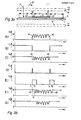
- FIG. 3a shows a sectional view in the line direction 13 through the transparent scanning table 1 and through the adhesive assembly located thereon, which in the example shown consists of the transparent template support 5 (transparent film) and a supervisory template 3 mounted on the template support 5.
- the original carrier 5 can, however, also be only slightly translucent (scattering translucent), which is the case, for example, with white paper.
- the information-carrying part 41 of the supervisory template 3 may be surrounded by a white border 42.
- the supervisory pre Layer 3 has mounting edges or shadow edges 43.
- FIG. 3b shows the signal curves in diagrams A) to G) which arise when the adhesive assembly is scanned in the row direction 13.
- Diagram A shows the image signal U Bf obtained from the upper scanner 14, which delivers the actual image information during the top-up scan.
- the detection signal U Z generated by the lower scanner 15 appears in diagram B).
- Diagram C) first shows the addition of the image signal U B and the detection signal U z in the adding stage 34 of the compensation circuit 18 in order to obtain the modified image signal U B '.
- the areas 44 and 45 of the template carrier 5 lying outside the supervisory template 3 are reproduced as "white”.
- the signal dips 46 are still present, which would appear as "black” or as a shadow during the re-recording.
- Diagram D) shows the trigger pulses U Z 'generated in the pulse shaper stage 37, which occur each time there is a change from supervision to transparency or vice versa, and the possible presence of shadow edges signal.
- Diagram E) shows the control pulses U Z "of duration 2 obtained in the monostable multivibrator.
- Diagram F shows the image signal U ' B' delayed in the delay stage 35 by the time period -1 , which is fed to the memory stage 36.
- Diagram G shows the result of the shadow edge suppression with the aid of the storage stage 36 on the basis of the image signal U B * , which is finally recorded.
- the memory stage 36 has recorded the image signal values "white” obtained when the shadow edges occurred at the times t 1 and t 2 for the duration 2 of the control pulses U Z ", thereby advantageously eliminating the signal dips 46 in the image signal U B and thus the shadow edges were suppressed.
- the changeover switch 39 is in the position shown in broken lines.
- the upper scanner 14 supplies the additional information and the first scanning signal is the detection signal U Z.
- the lower scanner 15 supplies the actual image information and the second scanning signal is the image signal U B.
- the mode of operation of the compensation circuit 18 in the case of see-through scanning is explained on the basis of the graphic representation in FIG. 4.
- FIG. 4a again shows a sectional view in the line direction 13 through the transparent scanning table 1 and the adhesive assembly on it.
- the difference from FIG. 3a is that a see-through template 3 is now applied to the translucent template carrier 5.
- the see-through template may also have a scratch 48.
- FIG. 4b shows the signal profiles in diagrams A) to E) which arise when the adhesive assembly is scanned through in line direction 13.
- Diagram A) shows the image signal U B generated in the lower scanner 15 and diagram B) shows the detection signal U z obtained in the upper scanner 14.
- Diagram C shows the addition of image signal U B and detection signal U z in the addition stage 34 of the compensation circuit 18 in order to obtain the image signal U B '.
- a modified image signal U B and a modified detection signal U Z are produced , which are shown in diagrams D) and E) and correspond to diagrams A) and B) of FIG. 3b for supervisory scanning.
- a corresponding shadow edge suppression can also be carried out with the aid of the memory stage 36 even in the case of a transparent scan.
- the scanner 14 delivering the detection signal Uz (in the case of a top-up scan) or the scanner 15 (in the case of a see-through scan) can advantageously be used to generate a "dash" or "halftone" detection signal.
- a mark is applied to the original carrier 5, for example in the line direction 13, in front of the original to be marked, which is scanned by the corresponding scanner in order to obtain a corresponding recognition signal.
- a recognition signal can advantageously be generated for each template by providing the marks with a bar code which is read by the scanner and is evaluated.
- the bar code is also saved and makes it easier to find the image information of the individual templates in the memory.
- Figure 5 shows a further embodiment of the scanner, in which the scanner 14 and 15 compared to Figure 1 modified light receiving devices 14 "and 15".
- the light receiving devices have approximately the shape of half hollow cylinders, the light openings 50 and 51 of which face the scanning table 1.
- the light receiving device 14 also has a light entry opening 52 for the scanning beam 7 '.
- the entire inner surface of the light receiving devices 14" and 15 are designed as light receiving surfaces, which in turn consist of a plurality of partial surfaces 53.
- the partial surfaces 5 in the exemplary embodiment are the end faces 53 of optical fibers 54, which are not shown in detail or in full length in Figure 5.
- the optical fibers 54 are arranged such that the end faces 53 form approximately tangential surfaces of the half hollow cylinders all optical fibers 54, symbolized by "A” and “B”, combined to form an optical fiber bundle 55 or 56 (A + B), the other end faces of the optical fibers 54 together each having a light exit surface 57 or 58 for the
- the optoelectronic transducer 28 and 29, for example, in each case, is located on the light exit surfaces 57 and 58, respectively Form of fast photo multiplier, optically coupled, which generate the image signal U B or the detection signal UZ on line 16 or 17.
- the partial areas 53 can also be the light entry areas of photodiodes.
- the previously described embodiments of the Scanning devices are intended for flat-bed scanning devices and are designed in such a way that the light-receiving devices extend at least over the length of the scanning table 1, as can be seen from FIGS. 1 and 5.
- the scanning devices can also be used advantageously in drum scanning devices.
- the light receiving devices 14 '; 15 ′ or 14 ′′; 15 ′′ for example, as a hollow sphere or as part of a hollow sphere with the cross sections shown in FIGS. 1 and 5.
- the light receiving surfaces 22 and 23 are no longer slit-shaped, but rather circular or square.
- the cross-sectional transducers 24 and 25 are omitted, and the optoelectronic transducers 28 and 29 are arranged directly in the circular or square light receiving areas or connected via at least one optical fiber, with such drum scanning devices one of the light receiving devices being inside and the other outside of the scanning drum then moves axially past the scanning drum with the scanning light beam.
- the scanning devices can of course also be used for scanning colored adhesive assemblies.
- three cross-sectional transducers 24 and 25 are provided, the light entry surfaces of which total the light-receiving surfaces 22 and 23 of the light-receiving devices form.
- the light exit surfaces of the cross-section converters are coupled separately via three color dividers to three separate optoelectronic converters for the purpose of color separation of the scanning light, which generate the three color measurement signals.
- the optical fiber bundle led to the optoelectronic transducers is split up into at least three individual bundles, the optical fiber end faces of a single bundle each forming a separate light exit surface.
- the optical fiber bundle is divided in such a way that a triple of optical fibers, the end faces of which lie close together in the light receiving surface, are selected and each optical fiber of a triple is assigned to a single bundle.
- the three light exit surfaces are also coupled to three separate optoelectronic converters via three color splitters in order to generate the three color measurement signals.
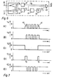
- FIG. 6 shows a further exemplary embodiment of a compensation circuit 18 'which can be used in line-glue assemblies.
- Image signal U B and detection signal U z are converted by means of level stages 61 and 62 into two-level signals U B 'and U Z ', the maximum amplitude of which corresponds to the white level and the minimum amplitude of which corresponds to the black level.
- the two-level signal U Z ' is converted in the pulse shaper stage 37 into a trigger pulse for the flip-flop 38, which generates a voltage pulse U Z "of pulse duration 2.
- the two-level signals U B ' and U Z 'and the voltage pulse U Z " arrive at an OR Gate 63, the output signal of which is the corrected image signal U B * .
- FIG. 7 shows a graphical representation to explain the mode of operation of the compensation circuit 18 'in the case of supervisory scanning.
- the image signal U B is again shown with the signal dips 46 due to shadow edges.
- Diagram B) shows the two-level image signal U a 'and diagram C) the two-level detection signal U Z ' at the outputs of level steps 61 and 62.
- Diagram D) shows the voltage pulses U Z "of pulse duration 2.
- Diagram E) shows the corrected image signal U B * at the output of the OR gate 63. It can be seen that the voltage dips 46 in the image signal U B have been eliminated by a logical OR operation of the signals.
Landscapes
- Engineering & Computer Science (AREA)
- Multimedia (AREA)
- Signal Processing (AREA)
- Facsimile Scanning Arrangements (AREA)
- Preparing Plates And Mask In Photomechanical Process (AREA)
- Facsimile Image Signal Circuits (AREA)
- Vehicle Body Suspensions (AREA)
- Container Filling Or Packaging Operations (AREA)
- Supplying Of Containers To The Packaging Station (AREA)
Priority Applications (5)
| Application Number | Priority Date | Filing Date | Title |
|---|---|---|---|
| EP82104843A EP0097724B1 (fr) | 1982-06-03 | 1982-06-03 | Procédé et dispositif de balayage |
| AT82104843T ATE15965T1 (de) | 1982-06-03 | 1982-06-03 | Abtastverfahren und abtasteinrichtung. |
| DE8282104843T DE3266654D1 (en) | 1982-06-03 | 1982-06-03 | Scanning method and arrangement |
| US06/497,509 US4568984A (en) | 1982-06-03 | 1983-05-24 | Method and apparatus for scanning masters |
| JP58092610A JPS592484A (ja) | 1982-06-03 | 1983-05-27 | 走査方法および走査装置 |
Applications Claiming Priority (1)
| Application Number | Priority Date | Filing Date | Title |
|---|---|---|---|
| EP82104843A EP0097724B1 (fr) | 1982-06-03 | 1982-06-03 | Procédé et dispositif de balayage |
Publications (2)
| Publication Number | Publication Date |
|---|---|
| EP0097724A1 true EP0097724A1 (fr) | 1984-01-11 |
| EP0097724B1 EP0097724B1 (fr) | 1985-10-02 |
Family
ID=8189067
Family Applications (1)
| Application Number | Title | Priority Date | Filing Date |
|---|---|---|---|
| EP82104843A Expired EP0097724B1 (fr) | 1982-06-03 | 1982-06-03 | Procédé et dispositif de balayage |
Country Status (5)
| Country | Link |
|---|---|
| US (1) | US4568984A (fr) |
| EP (1) | EP0097724B1 (fr) |
| JP (1) | JPS592484A (fr) |
| AT (1) | ATE15965T1 (fr) |
| DE (1) | DE3266654D1 (fr) |
Cited By (6)
| Publication number | Priority date | Publication date | Assignee | Title |
|---|---|---|---|---|
| EP0209119A2 (fr) * | 1985-07-16 | 1987-01-21 | Fuji Photo Film Co., Ltd. | Appareil d'analyse d'images |
| EP0215363A2 (fr) * | 1985-09-20 | 1987-03-25 | Linotype-Hell Aktiengesellschaft | Arrangement de balayage pour originaux à transmission demi-teinte |
| EP0384708A2 (fr) * | 1989-02-20 | 1990-08-29 | Sharp Kabushiki Kaisha | Dispositif de lecture optique |
| EP0524494A2 (fr) * | 1991-07-22 | 1993-01-27 | Eastman Kodak Company | Collecteur de lumière diffusée minimisant les distorsions de bandes |
| EP0816833A2 (fr) * | 1996-06-28 | 1998-01-07 | Fujifilm Electronic Imaging Limited | Dispositif et procédé d'illumination |
| WO2000046980A1 (fr) * | 1999-02-04 | 2000-08-10 | Applied Science Fiction | Dispositif et procedes pour la collecte de donnees relatives aux defauts |
Families Citing this family (32)
| Publication number | Priority date | Publication date | Assignee | Title |
|---|---|---|---|---|
| JPS60111634A (ja) * | 1983-11-19 | 1985-06-18 | 富士写真フイルム株式会社 | 放射線画像情報読取装置 |
| US5111308A (en) * | 1986-05-02 | 1992-05-05 | Scitex Corporation Ltd. | Method of incorporating a scanned image into a page layout |
| IL78675A (en) * | 1986-05-02 | 1993-02-21 | Scitex Corp Ltd | Color separation scanner |
| US5592309A (en) * | 1986-05-02 | 1997-01-07 | Scitex Corporation Ltd. | Multiple lens separation scanner |
| IL80242A (en) * | 1986-10-07 | 1994-01-25 | Scitex Corp Ltd | Laser scanner |
| US4743759A (en) * | 1986-10-14 | 1988-05-10 | Eastman Kodak Company | Light collector for photo-stimulable phosphor imaging system |
| US4742225A (en) * | 1986-10-16 | 1988-05-03 | Eastman Kodak Company | Elliptical cylinder light collector for photosimulable phosphor imaging apparatus |
| US5157516A (en) * | 1987-04-30 | 1992-10-20 | Scitex Corporation Ltd. | Method of incorporating a scanned image into a page layout |
| US4725893A (en) * | 1987-06-25 | 1988-02-16 | Eastman Kodak Company | Scanners |
| US4814630A (en) * | 1987-06-29 | 1989-03-21 | Ncr Corporation | Document illuminating apparatus using light sources A, B, and C in periodic arrays |
| US4868383A (en) * | 1988-09-08 | 1989-09-19 | Eastman Kodak Company | Linear integrating cavity light source used for generating an intense beam of light |
| US4899040A (en) * | 1988-09-08 | 1990-02-06 | Eastman Kodak Company | Light-conditioning apparatus for an image scanner illumination system |
| DE3877202D1 (de) * | 1988-10-14 | 1993-02-11 | Siemens Ag | Roentgendiagnostikeinrichtung mit einem speicherleuchtschirm. |
| US5282064A (en) * | 1989-08-31 | 1994-01-25 | Canon Kabushiki Kaisha | Apparatus for simultaneous reading of reflective and light conductive portions of an original |
| US5012346A (en) * | 1989-10-16 | 1991-04-30 | Eastman Kodak Company | Illumination system for a film scanner |
| US5103385A (en) * | 1990-07-27 | 1992-04-07 | Eastman Kodak Company | Linear light source |
| US5155596A (en) * | 1990-12-03 | 1992-10-13 | Eastman Kodak Company | Film scanner illumination system having an automatic light control |
| US5221840A (en) * | 1991-07-22 | 1993-06-22 | Eastman Kodak Company | Diffuse light collector |
| FR2681429B1 (fr) * | 1991-09-13 | 1995-05-24 | Thomson Csf | Procede et dispositif d'inspection du verre. |
| US5291392A (en) * | 1992-02-19 | 1994-03-01 | Gerber Systems Corporation | Method and apparatus for enhancing the accuracy of scanner systems |
| US5274228A (en) * | 1992-06-01 | 1993-12-28 | Eastman Kodak Company | Linear light source/collector with integrating cylinder and light pipe means |
| US5515182A (en) * | 1992-08-31 | 1996-05-07 | Howtek, Inc. | Rotary scanner |
| US5537164A (en) * | 1994-12-20 | 1996-07-16 | Smith; Alan D. | Retroilluminating indirect gonioprism |
| US5596190A (en) * | 1995-06-02 | 1997-01-21 | Minnesota Mining And Manufacturing Company | Light collection device for a film image digitizer |
| US5715051A (en) * | 1996-10-21 | 1998-02-03 | Medar, Inc. | Method and system for detecting defects in optically transmissive coatings formed on optical media substrates |
| US5910651A (en) * | 1997-07-15 | 1999-06-08 | Gerber Systems Corporation | Method and apparatus for image nonlinearity compensation in scanning systems |
| US5930433A (en) * | 1997-07-23 | 1999-07-27 | Hewlett-Packard Company | Waveguide array document scanner |
| US6587230B1 (en) * | 1998-09-30 | 2003-07-01 | Heidelberger Druckmaschinen Aktiengesellschaft | Apparatus for scanning masters |
| US6525844B1 (en) * | 1998-09-30 | 2003-02-25 | Heidelberger Druckmaschinen Aktiengesellschaft | Scanner device |
| US6580527B1 (en) * | 1998-09-30 | 2003-06-17 | Heidelberger Druckmaschinen Aktiengesellschaft | Method and arrangement for scanning masters |
| US6587229B1 (en) * | 1998-09-30 | 2003-07-01 | Heidelberger Druckmaschinen Aktiengesellschaft | Method and apparatus for scanning masters |
| JP2009092397A (ja) * | 2007-10-04 | 2009-04-30 | Nippon Avionics Co Ltd | 積分筒および積分筒を用いたライン型照明装置 |
Citations (4)
| Publication number | Priority date | Publication date | Assignee | Title |
|---|---|---|---|---|
| DE2356271A1 (de) * | 1972-11-13 | 1974-05-22 | Crosfield Electronics Ltd | Verfahren und vorrichtung zur bildreproduzierung |
| DE2423340A1 (de) * | 1973-05-16 | 1974-11-28 | Ilford Ltd | Abtastverfahren |
| DE2451570A1 (de) * | 1973-11-01 | 1975-05-15 | Ricoh Kk | Verfahren und vorrichtung zur faksimileuebertragung |
| DE2748325A1 (de) * | 1977-03-14 | 1978-12-14 | Dacom Inc | Beleuchtungs-kompensationsschaltung, insbesondere fuer eine bildabtastvorrichtung |
Family Cites Families (3)
| Publication number | Priority date | Publication date | Assignee | Title |
|---|---|---|---|---|
| US4468120A (en) * | 1981-02-04 | 1984-08-28 | Nippon Kogaku K.K. | Foreign substance inspecting apparatus |
| JPS5862543A (ja) * | 1981-10-09 | 1983-04-14 | Nippon Kogaku Kk <Nikon> | 欠陥検査装置 |
| DE3118459C2 (de) * | 1981-05-09 | 1984-01-26 | Dr.-Ing. Rudolf Hell Gmbh, 2300 Kiel | Lichtaufnahme-Vorrichtung |
-
1982
- 1982-06-03 AT AT82104843T patent/ATE15965T1/de not_active IP Right Cessation
- 1982-06-03 DE DE8282104843T patent/DE3266654D1/de not_active Expired
- 1982-06-03 EP EP82104843A patent/EP0097724B1/fr not_active Expired
-
1983
- 1983-05-24 US US06/497,509 patent/US4568984A/en not_active Expired - Fee Related
- 1983-05-27 JP JP58092610A patent/JPS592484A/ja active Granted
Patent Citations (4)
| Publication number | Priority date | Publication date | Assignee | Title |
|---|---|---|---|---|
| DE2356271A1 (de) * | 1972-11-13 | 1974-05-22 | Crosfield Electronics Ltd | Verfahren und vorrichtung zur bildreproduzierung |
| DE2423340A1 (de) * | 1973-05-16 | 1974-11-28 | Ilford Ltd | Abtastverfahren |
| DE2451570A1 (de) * | 1973-11-01 | 1975-05-15 | Ricoh Kk | Verfahren und vorrichtung zur faksimileuebertragung |
| DE2748325A1 (de) * | 1977-03-14 | 1978-12-14 | Dacom Inc | Beleuchtungs-kompensationsschaltung, insbesondere fuer eine bildabtastvorrichtung |
Cited By (13)
| Publication number | Priority date | Publication date | Assignee | Title |
|---|---|---|---|---|
| EP0209119A2 (fr) * | 1985-07-16 | 1987-01-21 | Fuji Photo Film Co., Ltd. | Appareil d'analyse d'images |
| EP0209119A3 (fr) * | 1985-07-16 | 1989-06-14 | Fuji Photo Film Co., Ltd. | Appareil d'analyse d'images |
| EP0215363A2 (fr) * | 1985-09-20 | 1987-03-25 | Linotype-Hell Aktiengesellschaft | Arrangement de balayage pour originaux à transmission demi-teinte |
| EP0215363A3 (en) * | 1985-09-20 | 1989-04-26 | Dr.-Ing. Rudolf Hell Gmbh | Scanning arrangement for half-tone transmission originals |
| US5126860A (en) * | 1989-02-20 | 1992-06-30 | Sharp Kabushiki Kaisha | Optical reading apparatus |
| EP0384708A3 (fr) * | 1989-02-20 | 1991-12-18 | Sharp Kabushiki Kaisha | Dispositif de lecture optique |
| EP0384708A2 (fr) * | 1989-02-20 | 1990-08-29 | Sharp Kabushiki Kaisha | Dispositif de lecture optique |
| EP0524494A2 (fr) * | 1991-07-22 | 1993-01-27 | Eastman Kodak Company | Collecteur de lumière diffusée minimisant les distorsions de bandes |
| EP0524494A3 (en) * | 1991-07-22 | 1993-04-14 | Eastman Kodak Company | A diffuse light collector which minimizes streak artifacts |
| EP0816833A2 (fr) * | 1996-06-28 | 1998-01-07 | Fujifilm Electronic Imaging Limited | Dispositif et procédé d'illumination |
| EP0816833A3 (fr) * | 1996-06-28 | 1998-08-26 | Fujifilm Electronic Imaging Limited | Dispositif et procédé d'illumination |
| US6091834A (en) * | 1996-06-28 | 2000-07-18 | Fujifilm Electronic Imaging, Limited | Method of illuminating a digital representation of an image |
| WO2000046980A1 (fr) * | 1999-02-04 | 2000-08-10 | Applied Science Fiction | Dispositif et procedes pour la collecte de donnees relatives aux defauts |
Also Published As
| Publication number | Publication date |
|---|---|
| ATE15965T1 (de) | 1985-10-15 |
| JPH0157546B2 (fr) | 1989-12-06 |
| US4568984A (en) | 1986-02-04 |
| DE3266654D1 (en) | 1985-11-07 |
| EP0097724B1 (fr) | 1985-10-02 |
| JPS592484A (ja) | 1984-01-09 |
Similar Documents
| Publication | Publication Date | Title |
|---|---|---|
| EP0097724B1 (fr) | Procédé et dispositif de balayage | |
| EP0065242B1 (fr) | Dispositif récepteur de lumière | |
| DE3118459C2 (de) | Lichtaufnahme-Vorrichtung | |
| DE2131467C3 (de) | Lichtablenkvorriehtung zur Parallelverschiebung eines Lichtstrahls | |
| DE2363455A1 (de) | Vorrichtung zur synchronisierung eines optischen abtasters | |
| DE3041184A1 (de) | Verfahren und vorrichtung zur bilderzeugung | |
| EP0065281B1 (fr) | Système d'analyse et diaphragme d'exploration pour la suppression de moiré pendant l'analyse d'originaux tramés | |
| DE3338868A1 (de) | Bildverarbeitungseinrichtung | |
| EP0120980A1 (fr) | Circuit de compensation de diaphonie dans des dispositifs d'analyse électro-optiques | |
| EP0038513B1 (fr) | Procédé et système de représentation d'une image d'un objet | |
| DE3443758C2 (fr) | ||
| DE3518608A1 (de) | Verfahren und vorrichtung zum steigern der aufloesung einer schar von sensoren | |
| DE3521682A1 (de) | Verfahren zum abtasten und aufzeichnen von bildern | |
| DE2752886C2 (de) | Belichtungskopf für ein Bildwiedergabegerät | |
| DE2518615C2 (de) | Kombiniertes Faksimile- und Kopiergerät | |
| EP0038514B1 (fr) | Procédé et système de détermination des lignes de démarcation entre deux surfaces de densité de couleur différente | |
| DE1762084C3 (de) | Vorrichtung zur Analyse einer Vorlage und zur Wiedergabe eines Bildes | |
| DE3933065C2 (fr) | ||
| DE2521089C3 (de) | Verfahren und Vorrichtung zum gleichzeitigen oder wahlweisen Abtasten einer Vorlage in einer Abtaststation und bzw. oder Aufzeichnen in einer Druckstation mittels derselben Laserlichtquelle | |
| DE3920669C2 (fr) | ||
| DE3445342A1 (de) | Laserstrahlbelichtungssystem | |
| DE3217752C2 (de) | Abtastverfahren und Abtastblende zur Vermeidung von Moiré in der Reproduktionstechnik | |
| DE3044217C2 (fr) | ||
| DE1772687C (de) | Verfahren und Vorrichtung zur Reproduktion von Halbtonbildern | |
| DE2065625C3 (de) | Abtasteinrichtung für ein Bildtelegrafiegerät |
Legal Events
| Date | Code | Title | Description |
|---|---|---|---|
| PUAI | Public reference made under article 153(3) epc to a published international application that has entered the european phase |
Free format text: ORIGINAL CODE: 0009012 |
|
| 17P | Request for examination filed |
Effective date: 19830402 |
|
| AK | Designated contracting states |
Designated state(s): AT BE CH DE FR GB IT LI NL SE |
|
| RBV | Designated contracting states (corrected) |
Designated state(s): AT BE CH DE FR GB IT LI NL SE |
|
| ITF | It: translation for a ep patent filed |
Owner name: STUDIO TORTA SOCIETA' SEMPLICE |
|
| GRAA | (expected) grant |
Free format text: ORIGINAL CODE: 0009210 |
|
| AK | Designated contracting states |
Designated state(s): AT BE CH DE FR GB IT LI NL SE |
|
| REF | Corresponds to: |
Ref document number: 15965 Country of ref document: AT Date of ref document: 19851015 Kind code of ref document: T |
|
| REF | Corresponds to: |
Ref document number: 3266654 Country of ref document: DE Date of ref document: 19851107 |
|
| ET | Fr: translation filed | ||
| PGFP | Annual fee paid to national office [announced via postgrant information from national office to epo] |
Ref country code: AT Payment date: 19860618 Year of fee payment: 5 |
|
| PLBE | No opposition filed within time limit |
Free format text: ORIGINAL CODE: 0009261 |
|
| STAA | Information on the status of an ep patent application or granted ep patent |
Free format text: STATUS: NO OPPOSITION FILED WITHIN TIME LIMIT |
|
| 26N | No opposition filed | ||
| PGFP | Annual fee paid to national office [announced via postgrant information from national office to epo] |
Ref country code: NL Payment date: 19870630 Year of fee payment: 6 |
|
| PG25 | Lapsed in a contracting state [announced via postgrant information from national office to epo] |
Ref country code: AT Effective date: 19880603 |
|
| PG25 | Lapsed in a contracting state [announced via postgrant information from national office to epo] |
Ref country code: LI Effective date: 19880630 Ref country code: CH Effective date: 19880630 |
|
| BERE | Be: lapsed |
Owner name: RUDOLF HELL G.M.B.H. Effective date: 19880630 |
|
| PG25 | Lapsed in a contracting state [announced via postgrant information from national office to epo] |
Ref country code: NL Effective date: 19890101 |
|
| NLV4 | Nl: lapsed or anulled due to non-payment of the annual fee | ||
| REG | Reference to a national code |
Ref country code: CH Ref legal event code: PL |
|
| PG25 | Lapsed in a contracting state [announced via postgrant information from national office to epo] |
Ref country code: BE Effective date: 19890630 |
|
| PGFP | Annual fee paid to national office [announced via postgrant information from national office to epo] |
Ref country code: FR Payment date: 19920527 Year of fee payment: 11 |
|
| PGFP | Annual fee paid to national office [announced via postgrant information from national office to epo] |
Ref country code: SE Payment date: 19920617 Year of fee payment: 11 |
|
| ITTA | It: last paid annual fee | ||
| PG25 | Lapsed in a contracting state [announced via postgrant information from national office to epo] |
Ref country code: SE Effective date: 19930604 |
|
| REG | Reference to a national code |
Ref country code: GB Ref legal event code: 732E |
|
| PG25 | Lapsed in a contracting state [announced via postgrant information from national office to epo] |
Ref country code: FR Effective date: 19940228 |
|
| REG | Reference to a national code |
Ref country code: FR Ref legal event code: ST |
|
| EUG | Se: european patent has lapsed |
Ref document number: 82104843.6 Effective date: 19940110 |
|
| PGFP | Annual fee paid to national office [announced via postgrant information from national office to epo] |
Ref country code: DE Payment date: 19960509 Year of fee payment: 15 |
|
| PGFP | Annual fee paid to national office [announced via postgrant information from national office to epo] |
Ref country code: GB Payment date: 19960520 Year of fee payment: 15 |
|
| PG25 | Lapsed in a contracting state [announced via postgrant information from national office to epo] |
Ref country code: GB Effective date: 19970603 |
|
| GBPC | Gb: european patent ceased through non-payment of renewal fee |
Effective date: 19970603 |
|
| PG25 | Lapsed in a contracting state [announced via postgrant information from national office to epo] |
Ref country code: DE Free format text: LAPSE BECAUSE OF NON-PAYMENT OF DUE FEES Effective date: 19980303 |