EP0085753A1 - Système de transmission des impulsions de signaux digitaux pour des lignes de réseau de distribution à courant alternatif - Google Patents
Système de transmission des impulsions de signaux digitaux pour des lignes de réseau de distribution à courant alternatif Download PDFInfo
- Publication number
- EP0085753A1 EP0085753A1 EP82109761A EP82109761A EP0085753A1 EP 0085753 A1 EP0085753 A1 EP 0085753A1 EP 82109761 A EP82109761 A EP 82109761A EP 82109761 A EP82109761 A EP 82109761A EP 0085753 A1 EP0085753 A1 EP 0085753A1
- Authority
- EP
- European Patent Office
- Prior art keywords
- chirp
- signal
- input
- output
- frequency
- Prior art date
- Legal status (The legal status is an assumption and is not a legal conclusion. Google has not performed a legal analysis and makes no representation as to the accuracy of the status listed.)
- Ceased
Links
Images


Classifications
-
- H—ELECTRICITY
- H04—ELECTRIC COMMUNICATION TECHNIQUE
- H04L—TRANSMISSION OF DIGITAL INFORMATION, e.g. TELEGRAPHIC COMMUNICATION
- H04L5/00—Arrangements affording multiple use of the transmission path
- H04L5/02—Channels characterised by the type of signal
- H04L5/06—Channels characterised by the type of signal the signals being represented by different frequencies
-
- H—ELECTRICITY
- H04—ELECTRIC COMMUNICATION TECHNIQUE
- H04B—TRANSMISSION
- H04B3/00—Line transmission systems
- H04B3/54—Systems for transmission via power distribution lines
- H04B3/542—Systems for transmission via power distribution lines the information being in digital form
-
- H—ELECTRICITY
- H04—ELECTRIC COMMUNICATION TECHNIQUE
- H04B—TRANSMISSION
- H04B2203/00—Indexing scheme relating to line transmission systems
- H04B2203/54—Aspects of powerline communications not already covered by H04B3/54 and its subgroups
- H04B2203/5404—Methods of transmitting or receiving signals via power distribution lines
- H04B2203/5416—Methods of transmitting or receiving signals via power distribution lines by adding signals to the wave form of the power source
-
- H—ELECTRICITY
- H04—ELECTRIC COMMUNICATION TECHNIQUE
- H04B—TRANSMISSION
- H04B2203/00—Indexing scheme relating to line transmission systems
- H04B2203/54—Aspects of powerline communications not already covered by H04B3/54 and its subgroups
- H04B2203/5404—Methods of transmitting or receiving signals via power distribution lines
- H04B2203/542—Methods of transmitting or receiving signals via power distribution lines using zero crossing information
-
- H—ELECTRICITY
- H04—ELECTRIC COMMUNICATION TECHNIQUE
- H04B—TRANSMISSION
- H04B2203/00—Indexing scheme relating to line transmission systems
- H04B2203/54—Aspects of powerline communications not already covered by H04B3/54 and its subgroups
- H04B2203/5404—Methods of transmitting or receiving signals via power distribution lines
- H04B2203/5425—Methods of transmitting or receiving signals via power distribution lines improving S/N by matching impedance, noise reduction, gain control
-
- H—ELECTRICITY
- H04—ELECTRIC COMMUNICATION TECHNIQUE
- H04B—TRANSMISSION
- H04B2203/00—Indexing scheme relating to line transmission systems
- H04B2203/54—Aspects of powerline communications not already covered by H04B3/54 and its subgroups
- H04B2203/5462—Systems for power line communications
- H04B2203/5466—Systems for power line communications using three phases conductors
-
- H—ELECTRICITY
- H04—ELECTRIC COMMUNICATION TECHNIQUE
- H04B—TRANSMISSION
- H04B2203/00—Indexing scheme relating to line transmission systems
- H04B2203/54—Aspects of powerline communications not already covered by H04B3/54 and its subgroups
- H04B2203/5462—Systems for power line communications
- H04B2203/5483—Systems for power line communications using coupling circuits
-
- H—ELECTRICITY
- H04—ELECTRIC COMMUNICATION TECHNIQUE
- H04B—TRANSMISSION
- H04B2203/00—Indexing scheme relating to line transmission systems
- H04B2203/54—Aspects of powerline communications not already covered by H04B3/54 and its subgroups
- H04B2203/5462—Systems for power line communications
- H04B2203/5491—Systems for power line communications using filtering and bypassing
Definitions
- the invention relates to a system for transmitting digital signal pulses over lines of an AC power distribution network, predominantly opposite to the direction of flow of the network energy, using a "chirp" frequency modulation and the frequency division multiplexing method and a synchronization of the signal generation in a transmitter and the signal processing in a receiver using the frequency of the AC mains voltage.
- FIG. 1 The block diagram of a transmission system shown in FIG. 1 shows a three-phase AC distribution network, a center 1 and at least one sub-station 2.
- a high voltage 3 of, for example, 50 kV and a frequency of 50 or 60 Hz is fed via a high-voltage switch 4 and a first transformer 5 an upper, also three-phase medium voltage level 6 with a voltage of 16.5 kV, for example.
- This medium-voltage level 6 is divided into several, for example three, three-phase "feeders" 7a, 7b and 7c, each of these "feeders” having its own three-pole medium-voltage switch 8a, 8b or 8c and its own, for example each consisting of three single-phase converters existing transducers 9a, 9b and 9c.
- These transducers can be current or voltage transformers. In Fig. 1, the presence of current transformers was assumed.
- the secondary windings of the three single-phase converters of each of the three measuring transformers 9a, 9b and 9c each feed a measuring circuit consisting of a measuring device, e.g. an ammeter, and one of the primary windings of a three-phase coupling converter.
- a measuring device e.g. an ammeter
- Each "feeder” 7a, 7b or 7c has such a three-phase, e.g. also associated with three single-phase converters coupling converters, which can be both a current and a voltage converter. Again, the presence of current transformers was assumed, the primary circuits of which are thus connected in series with the associated measuring device.
- the "feeder” 7a are e.g. the coupling converter 10 and the ammeter 11 assigned. 1 shows only one measuring circuit, namely the measuring circuit fed by the "feeder" 7a.
- the input of the control center 1 is located on the three secondary windings of the three-phase coupling converter 10.
- the "feeders" of the upper medium voltage level 6 are sometimes via their medium voltage switches 8a, 8b or 8c, the primary circuits of their measuring transformers 9a used as current transformers, 9b or 9c and a second transformer, for example in the "feeder” 7a via the second transformer 12, connected to a lower, likewise three-phase medium-voltage level, for example the medium-voltage level 13 in the case of the "feeder" 7a.
- This lower medium voltage level 13 carries, for example, a voltage of 4 kV.
- An insulation amplifier is connected in parallel to every second transformer in the opposite direction to the energy flow of the AC distribution network, for example in parallel to the second transformer 12 of the insulation amplifier 14.
- the lower medium-voltage level 13 of the "feeder” 7a feeds a low-voltage network 16 of e.g. 220 V.
- a low-voltage network 16 e.g. 220 V.
- sub-station 2 is connected in FIG. 1.
- this can alternatively be connected to the medium-voltage level 13 via a voltage converter (not shown).
- the control center 1 contains a known ripple control center 17, which via a ripple control transmitter 18, also known, via one of the "feeders” of the upper medium voltage level 6, e.g. Controls a known ripple control receiver 19 in the sub-station 2 via the "feeder” 7a, the lower medium-voltage level 13 and the low-voltage network 16.
- the ripple control devices mentioned form a known ripple control system, which is not the subject of a claim and is therefore not described in more detail. It is used here exclusively for the transmission of a call command from the central station 1 to the subordinate station 2. Therefore, the only output of the ripple control receiver 19 shown in FIG. 1 - the presence of a relay contact output was assumed - at the call input 20 of a telecontrol transmitter 21.
- the input of the ripple control receiver 19 and the output of the telecontrol transmitter 21 are connected to one another and to the low-voltage network 16 in the substation 2.
- the output signals of the telecontrol transmitter 21 reach the low-voltage Nu ngsnetz 16, the lower medium voltage level 13, the "feeder” 7a, the transducer 9a and the coupling converter 10, the input of the control center 1, which is also the input of a telecontrol receiver 22, the output of which in turn controls the input of a telecontrol evaluation device 23 .
- Substation 2 also contains a control circuit 24, a conditioning circuit 25, a measured value input bus 26, a counted value input bus 27, a message input bus 28 and a reset circuit 29.
- a system clock output 30 and a system clock input 31 are also indicated.
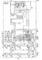
- FIG. 2 A block diagram of the processing circuit 25 is shown in FIG. 2.
- the system clock input 31 of the conditioning circuit 25 is fed by the mentioned system clock output 30 of the control circuit 24 with a system clock frequency of 2 MHz, and is at the same time the input of a frequency divider 32 which divides this frequency by four.
- This frequency divider 32 is constructed by means of a cascade of two flip-flop 32a and 32b, for example of type 74LS74 and has two 90 0 phase shifted 500 kHz outputs.
- the two interconnected clock inputs of these two flip-flops form the input of the frequency divider, and the Q-output of the first flip-flop 32a controls the D-input of the subsequent second flip-flop 32b, while its Q-output in turn is connected to the D-input of the first Flip flop 32a is fed back.
- An output signal in phase with the input signal of the frequency divider 32 appears at the Q output of the first flip-flop 32a and is connected to the clock input T of a counting chain 33, and the signal phase-shifted by 90 0 at the Q output of the second Flip-flop 32b feeds a ramp clock input R of a first transformer circuit 34.
- the system clock frequency of 2 MHz also reaches the clock input of a Johnson counter 36 via a first input of a two-input AND gate 35, for example of the 74LS08 type, for example by means of a shift register of type 74LS164 and whose parallel outputs feed a decoder 37.
- the last bit of Johnson counter 36 is fed back to its data input.
- the decoder 37 is constructed by means of several And gates, for example of the 74LS08 type, and inverters, for example of the 74LS04 type.
- a first output of decoder 37 blocks the AND gate 35 via its second input, while a second output is connected to the clock inputs of first and second buffer memories 38 and 39, and a third output is connected to a control input of a current source 40.
- a blocking signal (first output) or release signals (second and third output) appear at the correct moment, which is predetermined by the Johnson counter 36.
- the sub-station 2 serves to acquire and transmit telecontrol information, preferably in the opposite direction to the direction of energy flow of the AC distribution network.
- One or more substations can be operated with one transmission channel.
- Every telegram contains all information.
- the measured value, the count value and the signal input bus 26, 27 and 28 are simultaneously the bus inputs of the same name of the processing circuit 25 (FIG. 2).
- Each input bus 26, 27 and 28 advantageously has an equal number, e.g. eight, lines. In this case, eight measurements, eight counts and eight messages can be transmitted.
- Each line of the measured value input bus 26 is assigned an analog measured value.
- the level of each of these measurements e.g. from 22 to 100 V or from 1 VA to 50 VA, in a corresponding level adjustment circuit 41a to 41g, each consisting of a resistor network with built-in potentiometer, to a voltage range of e.g. + 2 to - 2 V limited, then fed to the signal inputs of an analog multiplexer 43a via a first-order RC filter 42a to 42g, which is used to eliminate hum interference> 50 Hz.
- the measured value input signals are bi- or unipolar direct currents or direct voltages.
- the address inputs of the multiplexer 43a which are controlled by a control bus 43b, select the individual signal inputs of the multiplexer 43a one after the other during the time reserved for the measurement value evaluation in time-division multiplexing and switch through the prepared analog measured values there one after the other to the input of the subsequent one Buffer amplifier 44, which works as an impedance converter and, for example, a non-inverting amplifier with the amplification factor, which is constructed by means of an operational amplifier LM 301A One is.
- the high impedance input impedance keeps the load on the input circuit low.
- the output of the buffer amplifier 44 is connected to a first input of a sum amplifier 45 constructed by means of an operational amplifier LM 301A, the output of which in turn is the input of a voltage / time converter 46, e.g. of the type MC1405.
- This voltage / time converter 46 contains e.g. a voltage reference source, the output of which feeds a second input of the sum amplifier 45, so that the zero voltage of the circuit is shifted by a reference voltage set within the sum amplifier 45 by means of a potentiometer (not shown).
- the potentiometer is part of the sum amplifier 45 and the output voltage of the latter is e.g. 0 V to 2 V.
- the output of the voltage / time converter 46 feeds the counting chain 33, which e.g.
- a start signal supplied by the control bus 43b resets all the binary counters of the cascade circuit 47 and a "ramp” flip-flop 50 in the counting chain 33 to zero.
- the latter blocks, via a first input of a two-input enable gate 51, the 500 kHz ramp clock frequency present at its second input, which is simultaneously the ramp clock input R of the first transformer circuit 34, so that at the "ramp” input of the voltage / time converter 46 the logic value "0" is present.
- a "ramp controt" switch then applies a current proportional to the input voltage to the input of an integrator, the output voltage of which is accordingly increases continuously from zero until it reaches the threshold value of a downstream comparator. From this moment on, an enable flip-flop 52 is switched over from the output of the comparator, which is also the output of the voltage / time converter 46, via the second transformer circuit 48 in the counting chain 33, so that one of the 33 using the cascade circuit 47 Fixed integration time is calculated by counting 500 kHz clock pulses which are fed from the frequency divider 32 via the clock input T of the counting chain 33 to the clock inputs of the binary counters of the cascade circuit 47.
- the ramp clock input R of the first transformer circuit 34 is connected to a first input and the clock input T of the counter chain 33 to a second input of a two-input nand gate 53, which serves as a pulse shaper and whose output is the read input of the second transformer circuit 48 and the clock input of the Enable flip-flop 52 of the count chain 33 controls.
- a third to tenth parallel output of the cascade circuit 47 of the counter chain 33 form a digital 8-bit data bus, which is connected to a measured value output bus 55 of the processing circuit 25 via a first "tri-state" data selector 54 controlled by the control bus 43b.
- the count value and signaling circuits of the processing circuit 25 are constructed identically, since logic values "1" and "0" are present on each line of the count value and signal input bus 27 or 28.
- these are digital pulse sequences, the frequencies of which are proportional to the count values, and in the case of the messages, they are continuous digital signals.
- the count value input bus 27 feeds a first filter group 56, the outputs of which are the inputs of a first transformer group 57 and the outputs of which in turn are the inputs of one control the first detector group 58.
- the individual pulses of each pulse series at the output of the detector group 58 are then briefly stored in the first buffer memory 38 and then fed to a count value output bus 60 of the processing circuit 25 via a second "tri-state" data detector 59, which is also controlled by the control bus 43b.
- the signal input bus 28 in turn feeds in the order specified via a second filter group 61, a second transformer group 62, a second detector group 63, the second buffer memory 39 and a third "tri-state" data selector 64, which is also controlled by the control bus 43b a Metde output bus 68 of the conditioning circuit 25.
- All three data selectors 54, 59 and 64 are e.g. type 74LS257. Instead of these data selectors, the "ports" of a read / write memory can also be used.
- the third output of the decoder 37 controls the control input of the current source 40 at the correct moment, predetermined by the Johnson counter 36, the outputs of which in turn feed the first and second transformer groups 57 and 62.
- the second output of the decoder 37 also controls the clock inputs of the first and the second buffer memories 38 and 39 at the correct moment, which is predetermined by the Johnson counter 36.
- control bus 43b acts on the control inputs of the three data selectors 54, 59 and 64 and, at the given moment, puts these data selectors into operation one after the other in such a way that a single one of these data selectors is switched through.
- Each of the two filter groups 56 and 61, the two transformer groups 57 and 62 and the two detector groups 58 and 63 has a filter for each conductor of the count value or the signal input bus connection 27 and 28 and for each conductor couple a transformer or a detector.
- the current source 40 also contains a bipolar transistor for each pair of conductors in each of the two input bus connections 27 and 28. All of these transistors are controlled within the current source 40 by a common current source, not shown. The functioning of two lines within the count value or signal processing circuit with the associated power source can be seen from German patent specification 25 33 483 and is therefore not described further.
- FIG. 3 shows a circuit diagram of the analog / digital converter 49, consisting, as already mentioned, of the voltage / time converter 46, the first transformer circuit 34, the second transformer circuit 48 and the counter chain 33.
- the first pole of the primary winding of a second isolating transformer 69 is grounded via a first series resistor 70 and the second pole is connected to the positive pole of the DC supply voltage V cc via the collector-emitter path of a bipolar transistor 71.
- the base of the transistor 71 is connected to the read input of the second transformer circuit 48 via a base resistor 72 and, like the clock input of the release flip-flop 52 of the counting chain 33, is simultaneously sampled by the output of the Nand gate 53 with its 500 kHz output signal.
- the secondary winding of the second isolating transformer 69 is short-circuited via a first diode 73 in the forward direction and a low-impedance series resistor 74, ie this secondary circuit is low impedance.
- a large current therefore flows in it and accordingly also in the associated primary circuit, the transistor 71 of which is switched on because of the 500 kHz output signal of the Nand gate 53, which generates a voltage drop in the first series resistor 70, the size of which corresponds to a logic value " 1 "and, since it is located at the D input of the enable flip-flop 52, in this is saved.
- a first pole of the primary winding of a first isolating transformer 77 is connected to the positive pole of the DC supply voltage V cc via a low-impedance feed resistor 78, and the second pole receives a 500 kHz clock signal from the output of the enable gate 51, an input of this enable gate 51 As already mentioned, the output of the "ramp” flip flop 50 is released. If this contains the logic value "1", then a current flows briefly in the primary circuit and thus also in the secondary circuit of the first isolating transformer 77, which current is connected in series with the secondary winding of this first isolating transformer 77 in the forward direction. Diode 79 flows through a load consisting of an R / C parallel circuit 80.
- the "ramp control" switch is switched in the latter.
- the pole of the secondary winding of the first and second isolating transformers 77 and 69, not connected to a diode, are connected to one another and to the ground of the voltage / time converter 46.
- the Q output of the enable flip-flop 52 feeds the "enable” input of the cascade circuit 47.
- the control bus 43b reduced to a single line, is connected to the "clear” inputs of the latter and the "ramp” flip-flop 50.
- twelve parallel inputs of the cascade circuit 47 is e.g. the binary word "000000011110", and its "Load” input is controlled by a first control gate 82, the first input of which is at the Q output of the "ramp” flip-flop 50.
- the two lowest bits of the 12-bit counting chain 33 are not used. They only serve to keep the coupling error of the output signal of the voltage / time converter 46 low.
- the following 8 bits contain the measured value.
- the eleventh bit represents the sign of the measured value and the twelfth bit is e.g. a control bit.
- the "load” inputs of the binary counters of the cascade circuit 47 are activated via a second input of the first control gate 82, so that the next positive going edge of the binary counter clock frequency whose cascade circuit 47 is loaded with the value 1920, for example.
- the bias current for generating a minimal ramp in the voltage / time converter 46 is compensated. This value was chosen so that after 128 clock pulses the cascade circuit 47 returns to the initial position with a state 2048, which corresponds to the zero point of the analog / digital converter 49. This state represents the negative measured value at the end of the range.
- the corresponding digital value consists consistently of "0" and the sign is "1".
- the output of the eleventh bit sets the "ramp” flip-flop 50 via a first input of a second control gate 83 and its clock input, which enables the enable gate 51 by means of its Q output, so that the Ramp clock frequency reaches the first transformer circuit 34 serving for electrical isolation and, via this, a logic value "1" at the "ramp” input of the voltage / time converter 46 appears, so that its "ramp control" switch is actuated, thus separating the input of this converter from the input signal and supplying a constant reference current with the opposite sign to the integrator.
- the integrator output voltage which had been rising until then, now drops back to zero and reaches the comparator threshold value after a reduction time t 2 .
- the release flip-flop 52 With the next positive going edge of the counter clock frequency, the release flip-flop 52 is reset and blocks the counting chain. Since the maximum voltage which the integrator achieves after an integration time t 1 is dependent on the measured value and the inclination of the falling ramp is constant, the lowering time t 2 is proportional to the measured value at the input of the voltage / time converter 46. The measurement of the lowering time t 2 by means of the counter chain 33 and its 500 kHz clock frequency results in a digital value representing the analog measured value. Since the same counting chain 33 is used for the measurement of the two times t 1 and t 2 , the advantage is achieved that its clock frequency does not have to be absolutely precise. It should only remain constant during a measurement period (t 1 + t 2 ).
- the described analog / digital conversion provides, for example, the following relationships: This corresponds to a "two's complement binary" code.
- All flip-flops of the counter chain 33 are e.g. 74LS74 and all its control gates Nand gates 74LS00.
- the ramp clock input R of the first transformer circuit 34 lies above an inverter 84, e.g. of type 74LS06, at the second input of the two-input second control gate 83 and a logic value "1" at the D input of the "ramp” flip-flop 50.
- inverter 84 e.g. of type 74LS06
- FIG. 4 shows the control circuit 24 (from FIG. 1) consisting of a microprocessor 85, for example of the 8085 type from Intel, Santa Clara, California, and a control / memory circuit 86
- the count value and the signal output bus 55, 60 and 68 of the conditioning circuit 25 feed the control / memory circuit 86 and are all connected to a common data bus 87 within this circuit.
- the data outputs of a read-only memory 88 and a programmable read-only memory 89 as well as the data connections of a read / write memory 90 are connected to this common data bus 87, which feeds the internal bus 92 of the latter via a data buffer memory 91 of the microprocessor 85.
- the internal bus 92 is connected to the address output of the microprocessor 85 in the microprocessor 85 by means of bus connections in the specified order via an address register 93 and an address buffer memory 94.
- the latter controls the address inputs of the read-only memory 88, the programmable read-only memory 89, the read / write memory 90 and an address decoder 95 by means of bus connections.
- These memories and this decoder together form the control / memory circuit 86.
- the internal bus controls 92 in addition, in the order specified, by means of bus connections via an instruction register 96 and an instruction decoder 97, a control unit 98, the clock input of which is located at the output of a system oscillator 99 of the microprocessor 85.
- the control unit 98 in turn feeds the instruction connections of the address decoder 95, the bus output of which contains the control inputs of the read-only memory 88, the programmable read-only memory 89 and a "timer" contained in the read / write memory 90, and the control bus 43b of the processing circuit 25 controls.
- the output of the reset shade 29 is at the reset input 100 of the control unit 98 and its clock output at the system clock output 30 and at a clock input of the "timer" of the read / write memory 90.
- the internal bus 92 of the microprocessor 85 feeds its telegram output 102 via a series output circuit 101, which in turn, as shown in FIG 1 can be seen at a telegram input 103 of the telecontrol transmitter 21. Its baud clock output 104 (FIG. 1) is connected to a clock input 105 of the series output circuit 101.
- the series output circuit 101 contains, inter alia, a check bit encoder for generating "parity bits”.
- the internal bus 92 is also still connected via a bus connection to the data connections of an "arithmetic logic unit” (ALU) 106 which contains, among other things, an accumulator (not shown).
- ALU arithmetic logic unit
- the read / write memory 90 is e.g. type 8156 from Intel
- the read-only memory 88 e.g. an EPROM 2732 from the same company
- the programmable read-only memory 89 is e.g. constructed by means of a "Dual in line” switch and bus line driver of the 74LS368 type and the address decoder 95 by means of a gate of the "Low Power Schottky” series of the 74LS ....
- a USART can also be used in addition to the microprocessor 85 e.g. type 8251 from Intel can be used.
- the microprocessor 85 and the memory of the control / memory circuit 86 form a microcomputer, which functions as a central control unit for all functions of the substation 2.
- the sequence programs of the microcomputer are stored in the read-only memory 88 and the station-specific values, such as, for example, station number, baud rate, transmission time window, etc., are stored in the field-programmable read-only memory 89. All digital measured values, messages and counts are temporarily stored in the read / write memory 90 via the corresponding input bus connections of the control circuit 24 and the common data bus 87. The latter, however, since they are a pulse train appear, the frequency of which is proportional to the count value, only after they have been continuously added up in the accumulator of the "arithmetic logic unit" 106, ie have been counted during a specific registration period. After this, the frequency determined in this way is stored as a digital value in the read / write memory 90.
- the microcomputer requires a supply voltage V cc between 4.75 V and 5.25 V for proper operation.
- the reset circuit 29 blocks the microcomputer at a supply voltage V cc ⁇ 4.75 V. This reset circuit 29 is not the subject of a patent claim and is therefore not described in detail.
- the digital data stored in the read / write memory 90 are called up successively in time by the microprocessor 85 in the correct time window, the series output circuit 101 arranging the individual bits of the individual data values in series one after the other and adding “parity bits” to them in a known manner for test purposes . Its individual bits thus reach one another in time at the telegram output 102 of the control circuit 24.
- the data telegram thus created is generally preceded by a pre-telegram called from the programmable read-only memory 89 and likewise consisting of serial bits. This contains e.g. Information about the subordinate and the type of the following data.
- the telegrams of the various substations 2 are sent in time division multiplex, sequentially in time. For this purpose, a time window is assigned to each transmitter and programmed in via the programmable read-only memory 89. The transmission takes place thanks to the network-synchronous baud clock frequency at the clock input 105 of the series output circuit 101.
- the telecontrol transmitter 21 is shown. Its telegram input 103 controls via an error correction encoder 107 the control input of a logic multiplexer 108 and thereby switches a "0-chirp" signal at logic value "0" and a "1-chirp” signal at logic value "1” to its data output bus, which has a "chirp” buffer memory 109 is connected to the digital input of a digital / analog converter 110.
- the output of the telecontrol transmitter 21 is at the input of its line filter 111 and at the same time on the low-voltage network 16.
- the line filter 111 is e.g. a very selective two-stage active bandpass fitter which can be operated by means of an operational amplifier, e.g. of type LM358. It eliminates all ripple control and telecontrol signals as well as all interferers present in the low-voltage network 16, so that at its output and thus at the input of a downstream comparator 112, e.g. type LM311, the pure 50 Hz AC voltage appears.
- the comparator 112 converts the sine into a square wave voltage, the frequency of which is increased to 100 Hz in the frequency doubler 113 connected downstream. This, e.g.
- phase shifter 114 constructed using two monostable multivibrators of the type 74LS221 and an OR gate 74LS32, in turn feeds a signal input of a phase shifter 114 with e.g. Rectangular pulses lasting 4 ⁇ s.
- the output frequency of this phase shifter 114 is divided by two, four and eight by means of a subsequent first divider chain, consisting in the order given of a first divider 115, a second divider 116 and a third divider 117, so that at the output of the phase shifter 114 the first divider 115, the second divider 116 and the third divider 117, the bit clock frequencies 100 Hz, 50 Hz and 12.5 Hz appear in the given order.
- One of these bit clock frequencies is selected as the baud clock frequency with the aid of a soldered first wire bridge 118 and switched on the baud clock output 104, which e.g. is an "open collector” output.
- This first divider chain consists e.g. from a "Divide by N counter” MC14018.
- a first local oscillator 119 with an output frequency of e.g. 204.8 Hz feeds both a clock input of the phase shifter 114, as well as the clock input of an address counter 120 and the input of a delay element 121.
- the local oscillator 119 is a known electrical circuit using a 4.9152 MHz crystal and several Nand gates, e.g. of type 74LS04, built up, the frequency of 4.9152 MHz thus generated in a downstream, not shown divider, consisting e.g. from a cascade connection of a "Divide by 12 counter" of the type 74LS92 and a flip-flop 74LS74, divided by twenty-four and thus giving the output frequency 204.8 kHz.
- One period of the 600 Hz frequency thus generated corresponds to one twelfth of the 50 Hz mains frequency, i.e. 30 °.
- an output flip-flop for example of the 74LS74 type, is set in the phase shifter 114, the Q output of which is the output of the phase shifter 114.
- This output flip-flop is then reset by the 204.8 kHz output signal of the first local oscillator 119.
- the input of phase shifter 114 is blocked by an internal release flip-flop until it is released again by a positive edge of the 100 Hz input signal. All other components of the phase shifter 114 are reset to their initial state when his output signal appears.
- the second local oscillator 123 is e.g. constructed using a 12.8 kHz crystal and several Nand gates of the type 74LS04 according to a known circuit of digital technology.
- the fourth divider 122 is e.g. a cascade connection of a "12 bit binary counter" of type MC14040 and two flip flops of type MC14013.
- the 25 Hz output frequency is divided in a downstream second divider chain, consisting of a fifth divider 124, a sixth divider 125, a seventh divider 126 and an eighth divider 127 in the order given.
- This output frequency is divided by 5 in the sixth divider 125, so that its output period is 5 minutes.
- the downstream seventh divider 126 in turn divides the output frequency of the sixth divider 125 by 3 so that its output period is 15 minutes, and the eighth divider 127 connected downstream of this seventh divider 126 divides its output frequency by 2 so that an output period of 30 minutes arises.
- one of the outputs of the fifth to eighth wires 124 to 127 is selected and connected to the base of a switching transistor 130 via a base resistor 129 and is used for the cyclical call of the remote control transmitter 21.
- the fifth divider 124 is e.g. from a cascade connection of three binary counters of the type MC14161 and the sixth to eighth divider 125 to 127 e.g. from such a binary counter MC14161.
- the parallel outputs of the address counter 120 are connected to the address input of a "chirp” read-only memory 131 via a bus connection.
- the output of the delay element 121 in turn feeds the clock input of the "chirp” buffer memory 109 and the digital output values of the logic multiplexer 108 are stored there for a short time with a delay.
- Both the “0-chirp” and the “1-chirp” signals are stored in the “chirp” read-only memory 131 and continuously reach a first and a second data input of the logic multiplexer 108 via a separate bus connection.
- the analog output of the digital / analog converter 110 controls the output of the telecontrol transmitter 21 via a first transmission filter 132, which serves to eliminate the digitization harmonics, a driver 133 serving for voltage amplification, a power amplifier 134 and a second transmission filter 135 for maintaining the Broadcasting interference regulations.
- the output of the telecontrol transmitter 21 is in turn connected via a relay contact 136a to the AC input of a power supply 137, the latter being at the call input 20 of the telecontrol transmitter 21 at the same time.
- the DC voltage output of the supply device 137 supplies the power amplifier 134 with its supply voltage.
- the emitter of the switching transistor 130 is grounded and its collector is connected to the positive pole of the DC supply voltage V cc via the relay coil 136b belonging to the relay contact 136a.
- the address counter 120 is e.g. MC14040 type, "Chirp” read only memory 131 e.g. type 2716 from Intel, and the "chirp" buffer 109 e.g. a "latch” of the type 74LS75.
- the delay element 121 is e.g. from two monostable multivibrators of type 74LS221 and the logic multiplexer 108 from AND gates e.g. type 74LS08.
- the two transmission filters 132 and 135 and the digital / analog converter 110 are e.g. built using LF353 operational amplifiers.
- the driver 133 and the power amplifier 134 are constructed by means of bipolar transistors and consist of known electronic circuits.
- error correction encoder 107 is optional. It creates e.g. a class (2,1) class, i.e. a coded double bit is generated from each uncoded bit. The easiest way to do this in a known manner is to use a shift register. A certain number of its parallel outputs generate the first bit of the double bit with the aid of a first excise-OR gate, and a certain number of other parallel outputs generate the second bit of the double bit with the aid of a second extractor-OR gate.
- the electrical signals forming the telegram are strongly attenuated in the transmission channel, i.e. in the AC supply network, e.g. due to losses in the transverse branches and in the series impedances, but especially in the third transformer 15, and on the other hand severely disturbed by interference frequencies, e.g. Mains harmonic and / or disturbance time pulses, so that voltage, frequency and / or phase distortions or holes can arise.
- interference frequencies e.g. Mains harmonic and / or disturbance time pulses
- S / N ratios signal-to-noise ratios
- the signal pulses represent, for example, the two logic values "1" and "0" and generally have the same frequency swing. They differ in the classic "chirp” modulation only in that the frequency deviation ranges for both logic values are different and not overlapping, and that an increasing mathematical function is used for one and a decreasing mathematical function for the other. Both logic signal pulses have - as was to be expected with frequency modulation - a very large, theoretically infinite bandwidth. This prevents the operation of many transmitters using the frequency division multiplex method on the same transmission path.
- An improvement is achieved through the use of a modified "chirp" modulation, the amplitude envelope of which is no longer constant during a pulse duration, but whose insertion and trailing edges are continuous, e.g. according to a cosine function, rise or fall.
- the duration of the edges is e.g. 15% each of the duration of the signal pulses, the amplitude envelope remaining constant and having the maximum value during the remaining 70% of the pulse duration.
- the duration of the edges can e.g. are also 60% of the signal pulse duration, in which case the duration of the constant maximum amplitude envelope is zero.
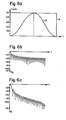
- the latter "chirp" modulation is compared in FIGS. 6a to 6c with the classic “chirp” modulation.
- FIG. 6a shows a normalized amplitude envelope U max of a classic "chirp” signal pulse A and a modified “chirp” signal pulse B, the latter with 50% settling and decay times, as a function of time t.
- 6b shows the only weakly damped, very broadband frequency spectrum D A of the classic "chirp” signal pulse A as a function of frequency f.
- 6c shows, also in radio tion of the frequency f, the very damped and therefore less broadband frequency spectrum D B of the modified "chirp" signal pulse B.
- 8 shows the signal relationships on the transmission path as a function of time t in diagrams 8a to 8e, but for the sake of simplicity assuming the use of classic "chirp" signal pulses with steep edges and constant amplitude envelopes, but with overlapping frequency swing.
- the baud rate was chosen to be 100 Bd for these diagrams. However, 50 baud, 25 baud, 12.5 baud and in the USA 120 baud, 60 baud, 30 baud and 15 baud are also possible in Europe.
- 8a shows a pure, undisturbed 50 Hz voltage u N of an AC supply network.
- 8b shows the undisturbed instantaneous voltage values u T of a "chirp" telegram, consisting, for example, of a double bit "10".
- Each bit start is synchronized with the zero crossings of the 50 Hz voltage u N , and each has the duration of half a period of the 50 Hz voltage u N , ie 10 ms, in the case of a 100 baud clock frequency.
- the undisturbed "chirp" telegram is shown again in FIG. 8c, but this time as instantaneous frequency values f T as a function of time t.
- the first bit with the logic value "1" begins with the frequency f ' 1 and rises linearly within 10 ms to the frequency f' 3 .
- the second bit with the logic value "0" begins with the frequency f ' 2 and ends after 10 ms with the frequency f' 4 , where f ' 1 ⁇ f' 2 ⁇ f ' 3 ⁇ f' 4 .
- FIG. 8d shows possible, strongly disturbed instantaneous voltage values u R
- FIG. 8e shows possible, strongly disturbed instantaneous frequency values f R of the "chirp" telegram, as can appear, for example, at the input of the telecontrol receiver 22.
- strong Stor time impulses are effective at points a and strong disturbance time pulse gaps at positions b.
- a strong interference frequency pulse is active at point c in bit "1" of FIG. 8e.
- the F i g. 9 reveals details of the telecontrol receiver 22, which is only indicated in FIG. 1.
- the coupling converter 10 feeds via the input of this receiver directly to the input of its received signal processing circuit 138, the output of which in turn directly drives the signal input of a quadrature demodulator 139.
- the output of the latter feeds directly to the analog input of an analog / digital converter 142, the status output of which controls the "sample and hold” switching input of the “sample and hold” circuit 141, and the digital output of which via a signal input bus 143 directly to the signal input one Receiver control circuit 144 is connected.
- the “sample and hold” circuit 141 is, for example, of the LF398 type and the analog / digital converter 142, for example of the AD ADC 80-12 type from Analog Devices, Norwood, Massachusetts, USA.
- the receiver control circuit 144 controls a first control input of the analog / digital converter 142 via a receiver control bus 145 and directly feeds a control input of the demodulator 139 via a receiver system clock output 146.
- a receiver reset circuit 147 is constructed in the same way as the reset circuit 29 of sub-station 2 (FIG. 1) performs the same function and directly controls a receiver reset input 148 of the receiver control circuit 144 with one pole.
- a 50 Hz or 60 Hz low voltage at the location of the control center 1 feeds a sine / square wave converter 150 via an impedance converter 149 with a high-impedance input, the rectangular output signal of which lies directly at the input of an adjustable receiver phase shifter 151.
- a first output of the latter is connected to a bit synchronization input of the demodulator 139 and a second output is connected to the input of a binary counter 152, the four parallel outputs of which feed a counting decoder 153.
- the output of the latter is connected to a second control input of the analog-digital converter 142.
- the Signal output of the receiver control circuit 144 feeds the output of the telecontrol receiver 22 in the specified order via an error correction decoder 155 , a check bit decoder 156 and a receiver buffer memory 157, its "level good" output 158 controls a first control input each and its clock output 159 each have a second control input of the error correction decoder 155, the check bit decoder 156 and the receiver buffer memory 157.
- the received signal conditioning circuit 138 indicated in FIG. 9 is shown in more detail in FIG. 10. It consists in the order given of a cascade connection of a sum or difference amplifier 161, a bandpass filter 162, a signal amplifier 163, a limiter stage 164, a pre-equalizer 165, a fine equalizer 166 and an "automatic gain control "Circuit 167, the output of the latter simultaneously being the output of the received signal conditioning circuit 138.
- the latter has the task of processing the possibly very strongly disturbed received signals at its input in accordance with FIGS. 8d and 8e in such a way that the signal deformations caused by the interferers and the non-ideal transmission properties of the transmission path are completely or at least partially reversed.
- the sum or difference amplifier 161 works on the one hand as a current / voltage converter and on the other hand forms the sum or the difference of the output voltages or currents e.g. of several phases of the output signal of the coupling converter 10 with the aid of an operational amplifier connected in a known manner as a sum or differential amplifier, e.g. type LF353.
- the bandpass filter 162 is e.g. a multi-stage, also known notch filter, which is also using several operational amplifiers, e.g. of type LF353, and eliminates all the frequency components of the interferers, which are outside the bandwidth of the undisturbed received signal.
- the limiter 164 After amplification in the preamplifier 163, the recom- f a ngssignal reached then the limiter 164.
- This also consists of an operational amplifier and is an inverting amplifier whose gain normally is ten, but which is shifted down in a known manner by means of diodes to three, if its input signal is too large, thus avoiding overdriving the subsequent circuits.
- the output signal of the limiter stage 164 reaches at a spatial distance of e.g. 100 m of the first four blocks of the receive signal processing circuit 138 from the rest of the system via a coaxial cable to the input of the downstream pre-equalizer 165, the function of which is to eliminate the distortions caused by the transmission path, primarily primarily phase and / or frequency distortions of the individual Frequencies of the transmitted signal as well as resonance peaks or holes to be reversed at least roughly.
- the phase or frequency equalization there is also an amplitude equalization, which in turn has a favorable effect on the signal / noise ratio.
- the pre-equalizer has adaptive capabilities since the telecontrol transmitters 21 can not only be located at different locations on the AC supply network, but also this network and its topology can change continuously over time. For this purpose, a number of e.g. ten "1" and "0" sent ahead.
- the subsequent fine equalizer 166 for example a "linear prediction filter", is used to eliminate all predictable, ie repetitive, interference components, that is to say in particular all periodic interference time pulses ("spikes") and the network harmonics.
- This fine equalizer 166 is only necessary in the case of very strong interference. It is most conveniently constructed using an adaptively controlled analog transversal filter based on a "Charged Coupted Device” (CCD).
- CCD Charge Coupted Device
- the subsequent "automatic gain control" circuit 167 regulates the input signal with a control constant of, for example, one to ten seconds at a constant level and represents a controller which is constructed, for example, by means of several LF353 operational amplifiers.
- FIG. 11 shows the quadrature demodulator 139 (FIG. 9), the input signal of which is equal to the processed reception signal at the output of the reception processing circuit 138 and in each case the input of a first mixer 168, a second mixer 169, and a third mixer 170 and a fourth mixer 171 is fed.
- An auxiliary oscillator 172 feeds a first reference generator 173 and a second reference generator 174.
- the former generates a "1" reference “chirp” signal pulse, for example in the same way as the telecontrol transmitter 21 generates its “chirp” signal pulses and the latter a "0" reference 'chirp "signal pulse, which feed a first and a second 90 phase shifter 175 and 176, respectively, in the order given.
- Each of these two 90 phase shifters 175 and 176 has two outputs: Am the first appears an output signal which is phase-shifted by 0 0 and the second an output signal which is phase-shifted by 90 0.
- These four output signals each feed the second input of one of the four mixers, namely the output signal of the first phase shifter 175 which is phase-shifted by 0 °, which is the first mixer 168 by 90 ° phase-shifted output signal the second mixer 169, the 0 ° phase-shifted output signal of the second phase shifter 176 the third mixer 170 and its by 90 0 phase displaced output signal the fourth mixer 171.
- the output of the first mixer 168 feeds a first input via a first low-pass filter 177, that of the second mixer 169 via a second low-pass filter 178 a second input, that of the third mixer 170 via a third Trefpassfuter 179 a third input and the- the fourth mixer 171 via a fourth low-pass filter 180 a fourth input of an analog demodulator multiplexer 181, the output of which in turn is connected to the output of the demodulator 139 via a computing circuit 182.
- the bitsynchroni The input of the demodulator 139 is connected to the respective synchronization input of the two reference generators 173 and 174.
- the analog demodulator multiplexer 181 has two poles and has two positions: in the first position the first and second inputs and in the second position the third and fourth inputs are connected to its two-pole output. The position of the demodulator multiplexer 181 is controlled via its control input.
- the two respective input signals ie the processed receive signal and one of the four reference "chirp" signals
- the demodulation is described a quadrature detection and uses two separate demodulations, a "1" for the received -Chirpsignal and one for the received "0" -Chirpsignal, and for each of the two demodulations two 90 0 phase shifted reference signals.
- the two demodulation signals thus generated indicate the amplitude of the received signal as well as its phase position with respect to the reference signal (vectors).
- Components ⁇ 1 and ⁇ 1 appear at the outputs of the first and second low-pass filters 177 and 178, and components ⁇ o and ⁇ o of the vectors appear at the outputs of the third and fourth low-pass filters 179 and 180. If the received signal is a "1" chirp signal, the components ⁇ 1 and ⁇ 1 dominate , whereas if it is a "0" chirp signal, the components ⁇ o and ⁇ o have the overweight. The value of the vectors is thus
- the demodulator multiplexer 18 for example of the type LF13201, successively conducts the value pairs ( ⁇ 1 , ⁇ 1 ) and ( ⁇ o , ⁇ o ) Calculation shading 182 to which the values calculated.
- the arithmetic circuit 182 is, for example, of the type BB4302 from Burr-Brown, Arlington, Arizona, USA. Demodulated analog values of the received signal thus appear at the output of the demodulator 139. At least one of the three parameters power, bandwidth and frequency is determined in the form of proportional electrical voltages from these analog values (see FIG. 9) in the subsequent PBF determination circuit 140.
- the receiver control bus 145 corresponds to the control bus 43b (FIG. 1), the receiver system clock output 146 to the system clock output 30 and the receiver reset input 148 to the reset input 100 (FIG. 4).
- the input corresponding to the clock input 105 of the control circuit 24 is not used here.
- the digitized received values of the signal input bus 143 are stored in the read / write memory of the receiver control circuit 144 and its microprocessor checks for each bit whether the "1" or the "0" chirp signal dominates and stores this write accordingly in a specific cell / Read memory from a logic value "1" or "0". These logic values are then successively read out in series and fed to the signal output of the receiver control circuit 144.
- a signal "level good” via the "level good” output 158 and a clock signal via the second clock output 159 are fed to the subsequent circuits and these are released on the one hand by the first signal and on the other hand provided with a clock frequency by the second signal. Both signals are generated or processed in the control unit of the receiver control circuit 144.
- the convolutional code (2, 1) is decoded in the error correction decoder 155 and possibly corrected with the aid of a known Viterbi decoder.
- the telegram obtained in this way is then subjected to a known "parity bit" check in the test bit decoder 156 and corrected if necessary, in order finally to be temporarily stored in the receiver buffer memory 157 for further evaluation.
- Impedance converter 149 is a non-inverting, e.g. amplifier built using an operational amplifier LM301 with a gain factor 1 and a high input impedance.
- Sine / Rectangle Converter 150 is a comparator e.g. type LM311.
- the adjustable receiver phase shifter 151 is e.g. constructed in the same way as the phase shifter 114 of the sub-station 2, except that an additional clock signal is connected via its second output to the clock input of the binary counter 152, which counts its pulses. The count value is then decoded in the count decoder 153, so that the subsequent analog / digital converter 142 is released at the right moment.
Landscapes
- Engineering & Computer Science (AREA)
- Signal Processing (AREA)
- Computer Networks & Wireless Communication (AREA)
- Power Engineering (AREA)
- Small-Scale Networks (AREA)
- Cable Transmission Systems, Equalization Of Radio And Reduction Of Echo (AREA)
- Measurement Of Resistance Or Impedance (AREA)
Applications Claiming Priority (2)
| Application Number | Priority Date | Filing Date | Title |
|---|---|---|---|
| CH696/82 | 1982-02-05 | ||
| CH69682 | 1982-02-05 |
Publications (1)
| Publication Number | Publication Date |
|---|---|
| EP0085753A1 true EP0085753A1 (fr) | 1983-08-17 |
Family
ID=4193030
Family Applications (1)
| Application Number | Title | Priority Date | Filing Date |
|---|---|---|---|
| EP82109761A Ceased EP0085753A1 (fr) | 1982-02-05 | 1982-10-22 | Système de transmission des impulsions de signaux digitaux pour des lignes de réseau de distribution à courant alternatif |
Country Status (4)
| Country | Link |
|---|---|
| EP (1) | EP0085753A1 (fr) |
| DK (1) | DK48783A (fr) |
| ES (1) | ES8403257A1 (fr) |
| NO (1) | NO830379L (fr) |
Cited By (6)
| Publication number | Priority date | Publication date | Assignee | Title |
|---|---|---|---|---|
| EP0348167A2 (fr) * | 1988-06-21 | 1989-12-27 | Canon Kabushiki Kaisha | Méthode et dispositif pour communication numérique |
| EP0419047A2 (fr) * | 1989-08-23 | 1991-03-27 | Intellon Corporation | Système de communication à spectre étalé utilisant une modulation à balayage de fréquence |
| EP0667695A4 (fr) * | 1991-08-23 | 1995-05-29 | Toshiba Kk | Systeme d'informations et de communications radio mettant en uvre un systeme de transmission a porteuses multiples et a etalement du spectre. |
| EP0924911A1 (fr) * | 1997-12-15 | 1999-06-23 | ABBPATENT GmbH | Procédé multiporteur de transmission sur des réseaux de distribution d'énergie |
| WO2000031899A1 (fr) * | 1998-11-24 | 2000-06-02 | Hughes Electronics Corporation | Synchronisation pour systeme de telephonie mobile par satellites utilisant un signal double chirp |
| CN104901573A (zh) * | 2014-11-19 | 2015-09-09 | 成都雷克尔科技有限公司 | 基于低通滤波的脉冲放大型逆变系统 |
Citations (1)
| Publication number | Priority date | Publication date | Assignee | Title |
|---|---|---|---|---|
| DE2727263B2 (de) * | 1977-05-17 | 1979-03-29 | Lgz Landis & Gyr Zug Ag, Zug (Schweiz) | System zur Signalübertragung über Leitungen eines Wechselstrom-Verteilungsnetzes, Einrichtung dazu und Anwendung des Verfahrens |
-
1982
- 1982-10-22 EP EP82109761A patent/EP0085753A1/fr not_active Ceased
-
1983
- 1983-02-04 ES ES519527A patent/ES8403257A1/es not_active Expired
- 1983-02-04 DK DK48783A patent/DK48783A/da not_active Application Discontinuation
- 1983-02-04 NO NO830379A patent/NO830379L/no unknown
Patent Citations (1)
| Publication number | Priority date | Publication date | Assignee | Title |
|---|---|---|---|---|
| DE2727263B2 (de) * | 1977-05-17 | 1979-03-29 | Lgz Landis & Gyr Zug Ag, Zug (Schweiz) | System zur Signalübertragung über Leitungen eines Wechselstrom-Verteilungsnetzes, Einrichtung dazu und Anwendung des Verfahrens |
Cited By (15)
| Publication number | Priority date | Publication date | Assignee | Title |
|---|---|---|---|---|
| EP0348167A2 (fr) * | 1988-06-21 | 1989-12-27 | Canon Kabushiki Kaisha | Méthode et dispositif pour communication numérique |
| EP0348167A3 (en) * | 1988-06-21 | 1990-06-13 | Canon Kabushiki Kaisha | Digital communicating method and apparatus |
| US5105294A (en) * | 1988-06-21 | 1992-04-14 | Canon Kabushiki Kaisha | Digital communicating method and apparatus |
| EP0419047A2 (fr) * | 1989-08-23 | 1991-03-27 | Intellon Corporation | Système de communication à spectre étalé utilisant une modulation à balayage de fréquence |
| EP0419047A3 (en) * | 1989-08-23 | 1992-10-21 | Intellon Corporation | Spread spectrum communications system using chirp modulation |
| US5574748A (en) * | 1989-08-23 | 1996-11-12 | Intellon Corporation | Spread spectrum communications system for network |
| EP0667695A1 (fr) * | 1991-08-23 | 1995-08-16 | Kabushiki Kaisha Toshiba | Systeme d'informations et de communications radio mettant en uvre un systeme de transmission a porteuses multiples et a etalement du spectre |
| US5561686A (en) * | 1991-08-23 | 1996-10-01 | Kabushiki Kaisha Toshiba | Radio information communication system using multi-carrier spread spectrum transmission system |
| EP0667695A4 (fr) * | 1991-08-23 | 1995-05-29 | Toshiba Kk | Systeme d'informations et de communications radio mettant en uvre un systeme de transmission a porteuses multiples et a etalement du spectre. |
| EP0924911A1 (fr) * | 1997-12-15 | 1999-06-23 | ABBPATENT GmbH | Procédé multiporteur de transmission sur des réseaux de distribution d'énergie |
| WO1999031852A1 (fr) * | 1997-12-15 | 1999-06-24 | Abb Patent Gmbh | Procede multisupports et dispositif pour sa mise en oeuvre |
| AU748265B2 (en) * | 1997-12-15 | 2002-05-30 | Abb Patent Gmbh | Multi-carrier method and device for implementing said method |
| WO2000031899A1 (fr) * | 1998-11-24 | 2000-06-02 | Hughes Electronics Corporation | Synchronisation pour systeme de telephonie mobile par satellites utilisant un signal double chirp |
| US6418158B1 (en) | 1998-11-24 | 2002-07-09 | Hughes Electronics Corporation | Synchronization in mobile satellite systems using dual-chirp waveform |
| CN104901573A (zh) * | 2014-11-19 | 2015-09-09 | 成都雷克尔科技有限公司 | 基于低通滤波的脉冲放大型逆变系统 |
Also Published As
| Publication number | Publication date |
|---|---|
| ES519527A0 (es) | 1984-03-01 |
| DK48783D0 (da) | 1983-02-04 |
| ES8403257A1 (es) | 1984-03-01 |
| DK48783A (da) | 1983-08-06 |
| NO830379L (no) | 1983-08-08 |
Similar Documents
| Publication | Publication Date | Title |
|---|---|---|
| DE69218652T2 (de) | Vorrichtung zur digitalen Datenübertragung über eine Leitung des Stromnetzes | |
| DE2013428C3 (de) | Anordnung zur uebertragung von daten im zeitmultiplexverfahren | |
| DE69227455T2 (de) | Binärdaten-fehlerkorrektur in einem modulierten signal mit hinweissignal auf vorgegebenen grenzwert überschreitende störgeräusche | |
| DD150824A5 (de) | Vorrichtung zur uebertragung von informationen auf einer wechselstromleitung | |
| DE2319569B2 (de) | Kabelf ernse hsystem | |
| DE2408151A1 (de) | Verfahren zur fernsteuerung ueber ein starkstromnetz und vorrichtung zur ausfuehrung des verfahrens | |
| EP0634842A2 (fr) | Procédé et dispositif de transmission bidirectionelle résistant aux perturbations pour réseaux d'alimentation électrique | |
| DE957312C (de) | Empfangsanordnung fuer ueber Hochspannungsleitungen gegebene Signale zur Verbesserung des Geraeuschabstandes | |
| EP0085753A1 (fr) | Système de transmission des impulsions de signaux digitaux pour des lignes de réseau de distribution à courant alternatif | |
| EP0058754B1 (fr) | Dispositif pour l'injection de signaux numériques dans un système filaire | |
| DE2249098B2 (de) | Verfahren und Vorrichtung zum Eliminieren von Entscheidungsfehlern infolge Intersymbol-Interferenz | |
| DE1189132B (de) | Schaltungsanordnung zur Pulsamplitudenmodulation und -demodulation | |
| EP0198263B1 (fr) | Montage pour la transmission de signaux numériques sans mise à la terre par l'intermédiaire de points de séparation | |
| DE2232299A1 (de) | Erweiterbarer multiplexer | |
| DE2130916B2 (de) | Übertragungsschaltung für digitale Signale | |
| DE960470C (de) | Elektrische Nachrichtenuebertragungsanlage mit Quantelung und mehrdeutigen Signalkennzeichen | |
| DE1762120A1 (de) | Einrichtung zur Dekodierung | |
| DE2104770A1 (de) | System zum Auswahlen eines Empfangers aus einer Anzahl von Empfangern | |
| DE2156873B2 (de) | Verfahren und vorrichtung zur fernsteuerung mittels den einzelnen befehlen zugeordneten impulsbildern | |
| DE4320930C2 (de) | Verfahren zur digitalen Signalübertragung | |
| DE2043144A1 (de) | Digitale Ubertragungsstrecke mit Re generativverstarkern | |
| DE2736522C2 (de) | Schaltungsanordnung zum Obertragen von Daten | |
| DE863672C (de) | Verfahren und Schaltungsanordnung zur UEbertragung von verschluesselten Reihen einpoliger elektrischer Impulse | |
| DE816106C (de) | Anordnung zur Verteilung von verschiedenen UEbertragungs-kanaelen angehoerenden Pulsen auf die einzelnen Kanaele und zu ihrer gleichzeitigen Demodulation | |
| DE900949C (de) | Einrichtung zur Umwandlung von P-Zyklus-Impulskodemodulation in Impulslagemodulation |
Legal Events
| Date | Code | Title | Description |
|---|---|---|---|
| PUAI | Public reference made under article 153(3) epc to a published international application that has entered the european phase |
Free format text: ORIGINAL CODE: 0009012 |
|
| AK | Designated contracting states |
Designated state(s): AT BE DE NL SE |
|
| 17P | Request for examination filed |
Effective date: 19831018 |
|
| STAA | Information on the status of an ep patent application or granted ep patent |
Free format text: STATUS: THE APPLICATION HAS BEEN REFUSED |
|
| 18R | Application refused |
Effective date: 19860217 |
|
| RIN1 | Information on inventor provided before grant (corrected) |
Inventor name: SCHMUCKI, PETER |