EP0084265A2 - Procédé pour la fabrication d'un dispositif semi-conducteur comportant une pluralité de régions monocristallines recristallisées - Google Patents
Procédé pour la fabrication d'un dispositif semi-conducteur comportant une pluralité de régions monocristallines recristallisées Download PDFInfo
- Publication number
- EP0084265A2 EP0084265A2 EP82306973A EP82306973A EP0084265A2 EP 0084265 A2 EP0084265 A2 EP 0084265A2 EP 82306973 A EP82306973 A EP 82306973A EP 82306973 A EP82306973 A EP 82306973A EP 0084265 A2 EP0084265 A2 EP 0084265A2
- Authority
- EP
- European Patent Office
- Prior art keywords
- layer
- single crystalline
- concave
- silicon
- insulating layer
- Prior art date
- Legal status (The legal status is an assumption and is not a legal conclusion. Google has not performed a legal analysis and makes no representation as to the accuracy of the status listed.)
- Granted
Links
Images


Classifications
-
- H—ELECTRICITY
- H01—ELECTRIC ELEMENTS
- H01L—SEMICONDUCTOR DEVICES NOT COVERED BY CLASS H10
- H01L21/00—Processes or apparatus adapted for the manufacture or treatment of semiconductor or solid state devices or of parts thereof
- H01L21/02—Manufacture or treatment of semiconductor devices or of parts thereof
- H01L21/02104—Forming layers
- H01L21/02365—Forming inorganic semiconducting materials on a substrate
- H01L21/02436—Intermediate layers between substrates and deposited layers
- H01L21/02439—Materials
- H01L21/02488—Insulating materials
-
- H—ELECTRICITY
- H01—ELECTRIC ELEMENTS
- H01L—SEMICONDUCTOR DEVICES NOT COVERED BY CLASS H10
- H01L21/00—Processes or apparatus adapted for the manufacture or treatment of semiconductor or solid state devices or of parts thereof
- H01L21/02—Manufacture or treatment of semiconductor devices or of parts thereof
- H01L21/02104—Forming layers
- H01L21/02365—Forming inorganic semiconducting materials on a substrate
- H01L21/02367—Substrates
- H01L21/0237—Materials
- H01L21/02373—Group 14 semiconducting materials
- H01L21/02381—Silicon, silicon germanium, germanium
-
- H—ELECTRICITY
- H01—ELECTRIC ELEMENTS
- H01L—SEMICONDUCTOR DEVICES NOT COVERED BY CLASS H10
- H01L21/00—Processes or apparatus adapted for the manufacture or treatment of semiconductor or solid state devices or of parts thereof
- H01L21/02—Manufacture or treatment of semiconductor devices or of parts thereof
- H01L21/02104—Forming layers
- H01L21/02365—Forming inorganic semiconducting materials on a substrate
- H01L21/02518—Deposited layers
- H01L21/02521—Materials
- H01L21/02524—Group 14 semiconducting materials
- H01L21/02532—Silicon, silicon germanium, germanium
-
- H—ELECTRICITY
- H01—ELECTRIC ELEMENTS
- H01L—SEMICONDUCTOR DEVICES NOT COVERED BY CLASS H10
- H01L21/00—Processes or apparatus adapted for the manufacture or treatment of semiconductor or solid state devices or of parts thereof
- H01L21/02—Manufacture or treatment of semiconductor devices or of parts thereof
- H01L21/02104—Forming layers
- H01L21/02365—Forming inorganic semiconducting materials on a substrate
- H01L21/02518—Deposited layers
- H01L21/02587—Structure
- H01L21/0259—Microstructure
- H01L21/02598—Microstructure monocrystalline
-
- H—ELECTRICITY
- H01—ELECTRIC ELEMENTS
- H01L—SEMICONDUCTOR DEVICES NOT COVERED BY CLASS H10
- H01L21/00—Processes or apparatus adapted for the manufacture or treatment of semiconductor or solid state devices or of parts thereof
- H01L21/02—Manufacture or treatment of semiconductor devices or of parts thereof
- H01L21/02104—Forming layers
- H01L21/02365—Forming inorganic semiconducting materials on a substrate
- H01L21/02656—Special treatments
- H01L21/02664—Aftertreatments
- H01L21/02667—Crystallisation or recrystallisation of non-monocrystalline semiconductor materials, e.g. regrowth
- H01L21/02675—Crystallisation or recrystallisation of non-monocrystalline semiconductor materials, e.g. regrowth using laser beams
-
- H—ELECTRICITY
- H01—ELECTRIC ELEMENTS
- H01L—SEMICONDUCTOR DEVICES NOT COVERED BY CLASS H10
- H01L21/00—Processes or apparatus adapted for the manufacture or treatment of semiconductor or solid state devices or of parts thereof
- H01L21/02—Manufacture or treatment of semiconductor devices or of parts thereof
- H01L21/02104—Forming layers
- H01L21/02365—Forming inorganic semiconducting materials on a substrate
- H01L21/02656—Special treatments
- H01L21/02664—Aftertreatments
- H01L21/02667—Crystallisation or recrystallisation of non-monocrystalline semiconductor materials, e.g. regrowth
- H01L21/02689—Crystallisation or recrystallisation of non-monocrystalline semiconductor materials, e.g. regrowth using particle beams
-
- H—ELECTRICITY
- H01—ELECTRIC ELEMENTS
- H01L—SEMICONDUCTOR DEVICES NOT COVERED BY CLASS H10
- H01L21/00—Processes or apparatus adapted for the manufacture or treatment of semiconductor or solid state devices or of parts thereof
- H01L21/70—Manufacture or treatment of devices consisting of a plurality of solid state components formed in or on a common substrate or of parts thereof; Manufacture of integrated circuit devices or of parts thereof
- H01L21/71—Manufacture of specific parts of devices defined in group H01L21/70
- H01L21/76—Making of isolation regions between components
- H01L21/762—Dielectric regions, e.g. EPIC dielectric isolation, LOCOS; Trench refilling techniques, SOI technology, use of channel stoppers
- H01L21/7624—Dielectric regions, e.g. EPIC dielectric isolation, LOCOS; Trench refilling techniques, SOI technology, use of channel stoppers using semiconductor on insulator [SOI] technology
- H01L21/76264—SOI together with lateral isolation, e.g. using local oxidation of silicon, or dielectric or polycristalline material refilled trench or air gap isolation regions, e.g. completely isolated semiconductor islands
- H01L21/76272—Vertical isolation by lateral overgrowth techniques, i.e. ELO techniques
Definitions
- the present invention relates to a method for producing a semiconductor device, more particularly to a method for producing a semiconductor device on a single crystallized region which is formed in a concave portion of an insulating later by melting polycrystalline silicon or amorphous silicon to flow therein.
- concave portions are formed in an insulating layer formed on a substrate, a polycrystalline silicon layer is formed on the insulating layer, and the polycrystalline silicon is melted by irradiation of a laser, electron beam, lamp, or other energy ray over the polycrystalline silicon layer to cause the polycrystalline silicon to flow into the concave portions, thereby forming single crystallized regions therein.
- a method for producing a semiconductor device comprising the steps of: forming an insulating layer on a substrate, said insulating layer having a plurality of concave portions respectively including a concave; forming a non-single crystalline silicon layer on a surface of said insulating layer; patterning said non-single crystalline silicon layer so that each concave portion is independently melting and flowing said patterned non-single crystalline silicon layer into said concave to form a single crystalline region in said concave by an irradiation with an energy ray; and forming a semiconductor element in said single crystalline region.
- an insulating layer 12 having a thickness of approximately 1 ⁇ m (micron) is formed on a silicon substrate 11 (Fig. lA).
- the insulating layer 12 is preferably selected from the group consisting of silicon dioxide, silicon nitride, oxi-nitride, and alumina.
- a photoresist layer 16 is formed on the insulating layer 12 and is exposed to ultraviolet rays or other energy rays 18 through a masking material 17, such as a glass mask (Fig. 1B).
- the exposed region of the photoresist layer 16 is hardened by development thereof and the unexposed portion is removed, thereby forming exposed portions 12a of the insulating layer 12 (Fig. 1C).
- the exposed portions 12a of the insulating layer 12 are etched to form concave portions 14a having a depth of, for example, 0.9 ⁇ m, i.e., a thickness (d) of 0.1 ⁇ m, and nonconcave portions 14b (Fig. 1D).
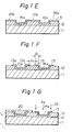
- a silicon layer 13 having a thickness of, for example, 0.4 ⁇ m is formed on the entire surface of the insulating layer 12, including the concave portion 14a and nonconcave portions 14b, by a chemical vapor deposition (CVD) process (Fig. IE).
- the silicon layer 13 is preferably selected from the group consisting of polycrystalline silicon and amorphous silicon.
- the silicon layer 13 is etched along the nonconcave portions 14b using, for example, a photoresist (not shown) as a masking material, to separate the layer 13 into different sections (Fig. 1F, Fig. 2).
- the width d 1 of the etched portion should be selected so that the amount of silicon in each section, i.e., the silicon remaining on the nonconcave portion 14b around each concave portion 14a (regions 13b), corresponding to the amount of width d 2 , and the silicon each concave portion 14a (regions 13a), equals the volume of the concave portion 14a.
- the width d 1 is selected to be 5 ⁇ m.
- a photoresist layer 20 is formed on the silicon layer 13 of the concave portions 14a to form the P channel regions (left portion Fig. 1G) and phosphorous ions are implanted in the silicon layers 13 of the concave portions 14a to form the N channel regions (right portion in Fig. 1G).
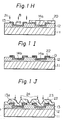
- the above photoresist layer 20 is removed, another photoresist layer 20 is formed on the silicon layers 13 to form the N channel regions (right portion in Fig. 1H), and bbron ions are implanted in the silicon layers 13 of the concave portions 14a to form the P channel regions (left portion in Fig. 1H).
- the above photoresist layer 20 is removed and the surfaces of the silicon layers 13 are thereby oxidized to form polyoxide layers 22 (Fig. lI).
- the polyoxide layers 22 prevent the doped ions from diffusing to portions other than the silicon layers 13.
- a capping insulating layer 23 of phosphosilicate glass or other materials of a thickness of approximately 1 ⁇ m over the entire surface of the insulating layer 12 and polyoxide layer 22.
- An energy ray 24, selected from the group of laser beams, electron beam, lamps, carbon heaters, etc., is then irradiated over the insulating layer 23 to the silicon layers 13.
- the regions 13a of the silicon layers 13 in the concave portions 14a of the insulating layers 12 melt earlier than the regions 13b on the nonconcave portions 14b because the former is proximity to the silicon substrate 11, which has act as a heat sink (Fig. 1J).
- the silicon of regions 13b next melts and flows into the concave portions 14a, leaving the cavities 25. It mixes with the silicon of regions 13a and is single crystallized as regions 26. Simultaneously, the previously implanted impurities for forming the N and P channel regions are uniformly distributed and activated (Fig. lK).
- the insulating layer 23 and polyoxide layer 22 are removed.
- the upper surface of the regions 26 is substantially level with, for example only about 0.12 ⁇ m higher than, the nonconcave portions 14b of the insulating layer 12 (Fig. 1L).
- C-MOS complementary metal oxide semiconductors
- IC bipolar integrated circuits
- metal semiconductor metal semiconductor
- junction and field effect transistor semiconductor display denies can be formed on the regions 26.
- a silicon layer 28 of a thickness of, for example, about 0.3 ⁇ m is formed on the insulating layer 27 by a CVD or other process (Fig. IN).
- the silicon layer 28 is etched using a masking material (not shown) to form gate electrodes 28 on the insulating layer 27 (Fig. 10).
- the surfaces of the gate electrodes 28 are oxidized to form thereon silicon dioxide layers 29 having a thickness of approximately 0.1 ⁇ m (Fig. lP).
- a photo mask 30 is formed on the P channel region, (left side in Fig. 1Q), and a 5 x 10 15 i ons/cm 2 dose of arsenic ions 21a are implanted in the N channel regions (right side in Fig. 1Q) with 150 KeV to form source region S and drain region D of MOS therein (Fig. 1Q).
- the above photo mask 30 is removed, after another photo mask 30 is similarly formed on the N channel region, and a 5 x 10 15 ions/cm 2 dose of boron ions 21b with 70 KeV are implanted in the P channel region to form source regin S and drain region D therein (Fig. 1R).
- insulating layers 31 are formed on the source regions S, drain regions D and insulating layers 29 by annealing (Fig. 1S).
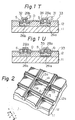
- a polycrystalline silicon layer 33 of a thickness of approximately 1 ⁇ m is formed on the insulating layers 12 and 31 (Fig. IT).
- the polycrystalline silicon layer 33 is etched at portions 34 to make contact holes on the source regions S and drain regions D.
- Aluminum wirings 35 are formed on the source regions S and drain regions D through the contact holes 34.
- a hole 40 penetrating to the silicon substrate 11 may be formed in the convex portion 14b of insulating layer 12, as shown in Fig. 3, so that the silicon of layer 43 is single crystallized with the same crystal orientation as that of the silicon substrate 11.
- another concave portion 51 may be formed at the bottom of the concave portion 14a, as shown in Fig. 4, so that the silicon positioned in the concave portion 51 melts and cools earlier than that in other portions and forms the nucleus for larger single crystalline silicon.
- a hole 61 penetrating to the silicon substrate 11 may be formed in the bottom of the concave portion 14a, as shown in Fig. 5, so that the area of the silicon substrate 11 positioned near the hole 61 forms the nucleus for single crystallization of the molten silicon.
- the process for producing a semiconductor device can be remarkably shortened.
Landscapes
- Engineering & Computer Science (AREA)
- Physics & Mathematics (AREA)
- Microelectronics & Electronic Packaging (AREA)
- General Physics & Mathematics (AREA)
- Manufacturing & Machinery (AREA)
- Computer Hardware Design (AREA)
- Condensed Matter Physics & Semiconductors (AREA)
- Power Engineering (AREA)
- Chemical & Material Sciences (AREA)
- Crystallography & Structural Chemistry (AREA)
- Materials Engineering (AREA)
- Optics & Photonics (AREA)
- Recrystallisation Techniques (AREA)
- Metal-Oxide And Bipolar Metal-Oxide Semiconductor Integrated Circuits (AREA)
- Element Separation (AREA)
Applications Claiming Priority (2)
| Application Number | Priority Date | Filing Date | Title |
|---|---|---|---|
| JP56211191A JPS58115832A (ja) | 1981-12-28 | 1981-12-28 | 半導体装置の製造方法 |
| JP211191/81 | 1981-12-28 |
Publications (3)
| Publication Number | Publication Date |
|---|---|
| EP0084265A2 true EP0084265A2 (fr) | 1983-07-27 |
| EP0084265A3 EP0084265A3 (en) | 1985-04-17 |
| EP0084265B1 EP0084265B1 (fr) | 1988-03-16 |
Family
ID=16601896
Family Applications (1)
| Application Number | Title | Priority Date | Filing Date |
|---|---|---|---|
| EP82306973A Expired EP0084265B1 (fr) | 1981-12-28 | 1982-12-24 | Procédé pour la fabrication d'un dispositif semi-conducteur comportant une pluralité de régions monocristallines recristallisées |
Country Status (4)
| Country | Link |
|---|---|
| US (1) | US5011783A (fr) |
| EP (1) | EP0084265B1 (fr) |
| JP (1) | JPS58115832A (fr) |
| DE (1) | DE3278259D1 (fr) |
Cited By (1)
| Publication number | Priority date | Publication date | Assignee | Title |
|---|---|---|---|---|
| EP0134504A1 (fr) * | 1983-07-15 | 1985-03-20 | Kabushiki Kaisha Toshiba | Dispositif CMOS et son procédé de fabrication |
Families Citing this family (4)
| Publication number | Priority date | Publication date | Assignee | Title |
|---|---|---|---|---|
| KR100189966B1 (ko) * | 1995-06-13 | 1999-06-01 | 윤종용 | 소이 구조의 모스 트랜지스터 및 그 제조방법 |
| US5914280A (en) * | 1996-12-23 | 1999-06-22 | Harris Corporation | Deep trench etch on bonded silicon wafer |
| US6004835A (en) | 1997-04-25 | 1999-12-21 | Micron Technology, Inc. | Method of forming integrated circuitry, conductive lines, a conductive grid, a conductive network, an electrical interconnection to anode location and an electrical interconnection with a transistor source/drain region |
| US5891763A (en) * | 1997-10-22 | 1999-04-06 | Wanlass; Frank M. | Damascene pattering of SOI MOS transistors |
Citations (3)
| Publication number | Priority date | Publication date | Assignee | Title |
|---|---|---|---|---|
| EP0030286A2 (fr) * | 1979-11-23 | 1981-06-17 | Alcatel N.V. | Dispositif semiconducteur à isolation diélectrique et procédé pour sa fabrication |
| EP0037261A1 (fr) * | 1980-03-27 | 1981-10-07 | Fujitsu Limited | Procédé de fabrication d'un dispositif semiconducteur et dispositif, p. ex. un BOMIS FET, réalisé selon ce procédé |
| EP0041776A2 (fr) * | 1980-05-14 | 1981-12-16 | Fujitsu Limited | Procédé pour la fabrication d'un dispositif semiconducteur comportant une structure d'isolation |
Family Cites Families (13)
| Publication number | Priority date | Publication date | Assignee | Title |
|---|---|---|---|---|
| US4174217A (en) * | 1974-08-02 | 1979-11-13 | Rca Corporation | Method for making semiconductor structure |
| JPS5530623A (en) * | 1978-08-25 | 1980-03-04 | Saburo Wakasugi | Vibration sensitive warning device |
| US4381201A (en) * | 1980-03-11 | 1983-04-26 | Fujitsu Limited | Method for production of semiconductor devices |
| JPS56144577A (en) * | 1980-04-10 | 1981-11-10 | Fujitsu Ltd | Production of semiconductor device |
| JPS577926A (en) * | 1980-06-18 | 1982-01-16 | Fujitsu Ltd | Manufacture of semiconductor device |
| US4372990A (en) * | 1980-06-23 | 1983-02-08 | Texas Instruments Incorporated | Retaining wall technique to maintain physical shape of material during transient radiation annealing |
| JPS5734331A (en) * | 1980-08-11 | 1982-02-24 | Toshiba Corp | Manufacture of semiconductor device |
| US4330363A (en) * | 1980-08-28 | 1982-05-18 | Xerox Corporation | Thermal gradient control for enhanced laser induced crystallization of predefined semiconductor areas |
| US4409724A (en) * | 1980-11-03 | 1983-10-18 | Texas Instruments Incorporated | Method of fabricating display with semiconductor circuits on monolithic structure and flat panel display produced thereby |
| US4448632A (en) * | 1981-05-25 | 1984-05-15 | Mitsubishi Denki Kabushiki Kaisha | Method of fabricating semiconductor devices |
| JPS5891621A (ja) * | 1981-11-26 | 1983-05-31 | Mitsubishi Electric Corp | 半導体装置の製造方法 |
| US4479847A (en) * | 1981-12-30 | 1984-10-30 | California Institute Of Technology | Equilibrium crystal growth from substrate confined liquid |
| US4473433A (en) * | 1982-06-18 | 1984-09-25 | At&T Bell Laboratories | Process for producing dielectrically isolated single crystal silicon devices |
-
1981
- 1981-12-28 JP JP56211191A patent/JPS58115832A/ja active Granted
-
1982
- 1982-12-24 EP EP82306973A patent/EP0084265B1/fr not_active Expired
- 1982-12-24 DE DE8282306973T patent/DE3278259D1/de not_active Expired
-
1990
- 1990-07-16 US US07/553,361 patent/US5011783A/en not_active Expired - Fee Related
Patent Citations (3)
| Publication number | Priority date | Publication date | Assignee | Title |
|---|---|---|---|---|
| EP0030286A2 (fr) * | 1979-11-23 | 1981-06-17 | Alcatel N.V. | Dispositif semiconducteur à isolation diélectrique et procédé pour sa fabrication |
| EP0037261A1 (fr) * | 1980-03-27 | 1981-10-07 | Fujitsu Limited | Procédé de fabrication d'un dispositif semiconducteur et dispositif, p. ex. un BOMIS FET, réalisé selon ce procédé |
| EP0041776A2 (fr) * | 1980-05-14 | 1981-12-16 | Fujitsu Limited | Procédé pour la fabrication d'un dispositif semiconducteur comportant une structure d'isolation |
Non-Patent Citations (1)
| Title |
|---|
| IEDM INTERNATIONAL ELECTRON DEVICES MEETING, Washington, D.C., 3rd-5th December 1979, Technical Digest, no. 9.2, IEEE, New York, USA; H.-W. LAM et al.: "Device and circuit fabrication and physical characterization of pulsed-laser-annealed polysilicon on SiO2 and Si3N4" * |
Cited By (2)
| Publication number | Priority date | Publication date | Assignee | Title |
|---|---|---|---|---|
| EP0134504A1 (fr) * | 1983-07-15 | 1985-03-20 | Kabushiki Kaisha Toshiba | Dispositif CMOS et son procédé de fabrication |
| US5079183A (en) * | 1983-07-15 | 1992-01-07 | Kabushiki Kaisha Toshiba | C-mos device and a process for manufacturing the same |
Also Published As
| Publication number | Publication date |
|---|---|
| DE3278259D1 (en) | 1988-04-21 |
| JPS58115832A (ja) | 1983-07-09 |
| EP0084265B1 (fr) | 1988-03-16 |
| EP0084265A3 (en) | 1985-04-17 |
| JPH0345530B2 (fr) | 1991-07-11 |
| US5011783A (en) | 1991-04-30 |
Similar Documents
| Publication | Publication Date | Title |
|---|---|---|
| US6248606B1 (en) | Method of manufacturing semiconductor chips for display | |
| EP0036137B1 (fr) | Procédé de fabrication de dispositifs à semi-conducteurs | |
| US20030211667A1 (en) | Method of fabricating thin film transistor | |
| KR20010074629A (ko) | 크기가 축소된 집적 회로의 제조에 사용하기에 적합한가스 주입 레이저 어닐링 방법 | |
| CN100356506C (zh) | 结晶掩模、非晶硅结晶方法及利用其制造阵列基板的方法 | |
| KR987000685A (ko) | 박막 회로를 구비한 전자 장치 제조 방법(Electronin device manufacture) | |
| US20020055207A1 (en) | Method for fabricating thin-film transistor | |
| EP0084265B1 (fr) | Procédé pour la fabrication d'un dispositif semi-conducteur comportant une pluralité de régions monocristallines recristallisées | |
| JPS622531A (ja) | 半導体装置の製造方法 | |
| EP0575965B1 (fr) | Procédé pour fabriquer un cristal semi-conducteur et dispositif semi-conducteur | |
| JPH07202209A (ja) | 薄膜トランジスタおよびその製造方法 | |
| JPH02864B2 (fr) | ||
| JP3027013B2 (ja) | 半導体における不純物のドーピング方法および半導体装置の製造方法 | |
| JPH0438140B2 (fr) | ||
| JPS6342417B2 (fr) | ||
| JPH02863B2 (fr) | ||
| KR100508023B1 (ko) | 엘디디형 다결정 규소 박막 트랜지스터 및 그 제조 방법 | |
| KR100249178B1 (ko) | 마스크롬 셀 및 그 제조방법 | |
| KR100504537B1 (ko) | 박막 트랜지스터의 제조 방법 | |
| KR100243276B1 (ko) | 레이저 어닐링을 이용한 다결정실리콘 박막의 제조방법 및 이를 이용한 박막 트랜지스터의 제조방법 | |
| JPH033247A (ja) | 薄膜トランジスタの製造方法 | |
| JPS6236854A (ja) | 半導体装置の製造方法 | |
| JP2005045036A (ja) | 結晶性膜の製造方法、結晶性膜、半導体薄膜、半導体装置および表示装置 | |
| JPH01264214A (ja) | 半導体装置の製造方法 | |
| JPH0462851A (ja) | 薄膜半導体装置の製造方法 |
Legal Events
| Date | Code | Title | Description |
|---|---|---|---|
| PUAI | Public reference made under article 153(3) epc to a published international application that has entered the european phase |
Free format text: ORIGINAL CODE: 0009012 |
|
| AK | Designated contracting states |
Designated state(s): DE FR GB |
|
| PUAL | Search report despatched |
Free format text: ORIGINAL CODE: 0009013 |
|
| AK | Designated contracting states |
Designated state(s): DE FR GB |
|
| 17P | Request for examination filed |
Effective date: 19851008 |
|
| 17Q | First examination report despatched |
Effective date: 19861121 |
|
| GRAA | (expected) grant |
Free format text: ORIGINAL CODE: 0009210 |
|
| AK | Designated contracting states |
Kind code of ref document: B1 Designated state(s): DE FR GB |
|
| REF | Corresponds to: |
Ref document number: 3278259 Country of ref document: DE Date of ref document: 19880421 |
|
| ET | Fr: translation filed | ||
| PLBE | No opposition filed within time limit |
Free format text: ORIGINAL CODE: 0009261 |
|
| STAA | Information on the status of an ep patent application or granted ep patent |
Free format text: STATUS: NO OPPOSITION FILED WITHIN TIME LIMIT |
|
| PGFP | Annual fee paid to national office [announced via postgrant information from national office to epo] |
Ref country code: DE Payment date: 19890227 Year of fee payment: 7 |
|
| 26N | No opposition filed | ||
| PG25 | Lapsed in a contracting state [announced via postgrant information from national office to epo] |
Ref country code: GB Effective date: 19891224 |
|
| GBPC | Gb: european patent ceased through non-payment of renewal fee | ||
| PG25 | Lapsed in a contracting state [announced via postgrant information from national office to epo] |
Ref country code: FR Effective date: 19900831 |
|
| PG25 | Lapsed in a contracting state [announced via postgrant information from national office to epo] |
Ref country code: DE Effective date: 19900901 |
|
| REG | Reference to a national code |
Ref country code: FR Ref legal event code: ST |