EP0081422B1 - Procédé collectif de fabrication de circuits logiques comportant au moins un transistor à effet de champ du type à faible tension de seuil, et une résistance saturable, et circuit logique réalisé par un tel procédé - Google Patents
Procédé collectif de fabrication de circuits logiques comportant au moins un transistor à effet de champ du type à faible tension de seuil, et une résistance saturable, et circuit logique réalisé par un tel procédé Download PDFInfo
- Publication number
- EP0081422B1 EP0081422B1 EP82402181A EP82402181A EP0081422B1 EP 0081422 B1 EP0081422 B1 EP 0081422B1 EP 82402181 A EP82402181 A EP 82402181A EP 82402181 A EP82402181 A EP 82402181A EP 0081422 B1 EP0081422 B1 EP 0081422B1
- Authority
- EP
- European Patent Office
- Prior art keywords
- transistor
- thickness
- saturable
- resistor
- threshold voltage
- Prior art date
- Legal status (The legal status is an assumption and is not a legal conclusion. Google has not performed a legal analysis and makes no representation as to the accuracy of the status listed.)
- Expired
Links
Images
Classifications
-
- H—ELECTRICITY
- H03—ELECTRONIC CIRCUITRY
- H03K—PULSE TECHNIQUE
- H03K19/00—Logic circuits, i.e. having at least two inputs acting on one output; Inverting circuits
- H03K19/02—Logic circuits, i.e. having at least two inputs acting on one output; Inverting circuits using specified components
- H03K19/08—Logic circuits, i.e. having at least two inputs acting on one output; Inverting circuits using specified components using semiconductor devices
- H03K19/094—Logic circuits, i.e. having at least two inputs acting on one output; Inverting circuits using specified components using semiconductor devices using field-effect transistors
- H03K19/0952—Logic circuits, i.e. having at least two inputs acting on one output; Inverting circuits using specified components using semiconductor devices using field-effect transistors using Schottky type FET MESFET
-
- H—ELECTRICITY
- H10—SEMICONDUCTOR DEVICES; ELECTRIC SOLID-STATE DEVICES NOT OTHERWISE PROVIDED FOR
- H10D—INORGANIC ELECTRIC SEMICONDUCTOR DEVICES
- H10D84/00—Integrated devices formed in or on semiconductor substrates that comprise only semiconducting layers, e.g. on Si wafers or on GaAs-on-Si wafers
- H10D84/01—Manufacture or treatment
- H10D84/0123—Integrating together multiple components covered by H10D12/00 or H10D30/00, e.g. integrating multiple IGBTs
-
- H—ELECTRICITY
- H10—SEMICONDUCTOR DEVICES; ELECTRIC SOLID-STATE DEVICES NOT OTHERWISE PROVIDED FOR
- H10D—INORGANIC ELECTRIC SEMICONDUCTOR DEVICES
- H10D84/00—Integrated devices formed in or on semiconductor substrates that comprise only semiconducting layers, e.g. on Si wafers or on GaAs-on-Si wafers
- H10D84/01—Manufacture or treatment
- H10D84/02—Manufacture or treatment characterised by using material-based technologies
- H10D84/05—Manufacture or treatment characterised by using material-based technologies using Group III-V technology
-
- H—ELECTRICITY
- H10—SEMICONDUCTOR DEVICES; ELECTRIC SOLID-STATE DEVICES NOT OTHERWISE PROVIDED FOR
- H10N—ELECTRIC SOLID-STATE DEVICES NOT OTHERWISE PROVIDED FOR
- H10N89/00—Integrated devices, or assemblies of multiple devices, comprising at least one bulk negative resistance effect element covered by group H10N80/00
Definitions
- the invention relates to a collective method for manufacturing logic circuits each comprising at least one field effect transistor of the almost normally blocked type or with low threshold voltage, and at least one saturable resistor integrated on the same semiconductor substrate as the transistor.
- normally conductive field effect transistors and normally blocked transistors are known in the conventional way.
- the former are blocked by depletion, requiring a double-polarity power supply and also having the drawback of consuming electrical current in the quiescent state.
- the second allow the current to flow when an appropriate voltage is applied to the control grid: they do not require a double polarity supply and are more economical, but on the other hand difficult to achieve, because of the very thin thickness of the conduction channel giving rise to a large amount of manufacturing waste.
- a third category of field effect transistors which is intermediate between the two preceding ones while approaching the second, is constituted by the transistors almost normally blocked or at low threshold voltage; they are blocked for a threshold voltage V T which can be positive or negative, which means that there is a certain dispersion in the collective manufacture of these transistors which is for example the following: or
- T. F.S. Almost normally blocked or low threshold voltage transistors, which will be designated hereinafter by the abbreviation T. F.S., are easier to manufacture than normally blocked transistors, but less easy to manufacture than normally conducting transistors. They fall between these two categories with regard to current consumption.
- T.F.S. transistors, and logic circuits using them by the technique described in the patent application of the Applicant FR-A-2449369, in which the field effect transistor of the T.F.S. type. comprises a trench dug by ion erosion between source and drain, the grid being deposited at the bottom of this trench.
- the logic circuits which use them include saturable resistors constituted by two ohmic contacts deposited on the active layer of the field effect transistor and separated by a trench dug by ion erosion in the active layer to a depth such that, in the remaining thickness of the active layer, it can form, for a given electric field, of the order of a volt, a dipolar domain similar to that which circulates in a structure with Gunn effect, but which is here stationary, as a result of the very small width of the trench (of the order of a micron), this range appearing for a very small value of the voltage existing at the terminals of the saturable resistance, voltage of the order of a volt.
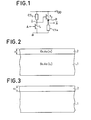
- FIG. 1 An example of a logic circuit comprising two T.F.S. and two saturable resistors of the type described above is shown in FIG. 1.
- a logic inverter is shown, the input A of which is connected to the gate of a transistor T 1 which is a TFS
- This transistor has its source at ground, its drain connected to point 1 itself connected to the hot point corresponding to a pole (positive in this example) of a source V DD through a resistive load CS 1 .
- the example chosen corresponds to the case of the n-channel transistor. For a p channel, the polarities must be reversed.
- the point 1 is connected to the gate of a transistor T 2 which is a TFS
- the transistor T 2 has its drain connected to the pole + V DD , its source to a diode D, passing in the direction going from + V DD to the mass.
- the return to ground is carried out through a resistive load CS 2 of the same type as CS 1 .
- the output A of the inverter is taken between D and CS z .
- the invention aims to overcome such subjection.
- the purpose of the manufacturing method according to the invention is the collective manufacturing of logic circuits each comprising at least one T.F.S. and saturable resistance.
- Fig. 1 already described above, represents an input A and output A logic inverter, having a first stage comprising a transistor T, and a saturable resistance CS ,, and an output stage comprising, in addition to a transistor T 2 and a saturable resistor CS 2 , a rectifier diode D.
- Fig. 9 shows the same type of reverser as in FIG. 1; but in which the saturable resistors are produced in the form of normally conducting transistors TS, and TS 2 with a grid connected to the source.
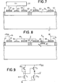
- a semiconductor wafer made of gallium arsenide (shown in partial cross section) comprises a substrate 1 and an active layer 2.
- the substrate 1 is made of insulating gallium arsenide with residual doping less than 10 3 atoms / cm 3 (or resistivity greater than 10 7 ⁇ -cm).
- the active layer 2, obtained for example by epitaxy, is of a thickness greater than 250 nm (2500 ⁇ ) with a maximum thickness variation of the order of 10 nm (100 ⁇ ) over 1 cm 2 . It is doped in the conductivity type n with a doping rate of around 1017 at / cm3.
- the result obtained at the end of step (b) has been shown during which the free surface of layer 2 has been attacked alternately to reduce the thickness of the latter.
- the desired result is a thickness a 1 of the order of 200 nm (2000 ⁇ ) with a predetermined doping profile controlled using a device commonly called "profilometer".
- the attack on the surface is carried out either by anodic oxidation, or by ion erosion, or by the action of a specific plasma of the material.
- the profilometer makes it possible to determine, by a measurement of electrical capacity, the depth of the deserted area under a DC voltage of predetermined value.
- the measuring device makes it possible to plot the curve (or profile) of the thickness of the deserted area as a function of this voltage.
- step (c) the result obtained at the end of step (c) has been shown in the case of implantation of ions such as H + , B + and O + having the effect of creating very high density defects in the crystal lattice, thus forming insulating barriers 41, 42 and 43 provided here to isolate the two components of the first stage of a circuit such as that of FIG. 1 or 9.
- step (d) of the process in which, for example using photosensitive resin, a preliminary masking has been carried out so as to produce deposits capable of producing with arsenide of gallium of the ohmic contacts (gold-germanium alloy for example), thus forming the contacts 51 and 52 for the saturable resistance, 53 and 54 for the transistor with TFS
- step (e) the result obtained in step (e) is shown by successive deposits of metals such as titanium, platinum and gold.
- a Schottky contact 62 is thus obtained located between the contacts 51 and 52.
- the ohmic contacts of the previous step receive the same metallic deposits, hence the formation of complementary metallizations 61, 63 on the contacts 51 and 52, 64 and 65 on contacts 53 and 54.
- the value a o is determined by taking into account the results of the measurements carried out in step (b), and possibly in the additional step, inserted after step (e).
- step (h) for example by a process analogous to that of step (e), a Schottky contact 82 is deposited in the trench 81.
- step (i) in the form of metallizations 83 (joining the drain 61 to the pole + V DD of the logic circuit 84) connecting the contacts 62, 63 and 64, finally 85 going from the contact 65 to ground.
Landscapes
- Engineering & Computer Science (AREA)
- Power Engineering (AREA)
- Physics & Mathematics (AREA)
- Computer Hardware Design (AREA)
- Computing Systems (AREA)
- General Engineering & Computer Science (AREA)
- Mathematical Physics (AREA)
- Semiconductor Integrated Circuits (AREA)
- Junction Field-Effect Transistors (AREA)
- Design And Manufacture Of Integrated Circuits (AREA)
- Logic Circuits (AREA)
Applications Claiming Priority (2)
| Application Number | Priority Date | Filing Date | Title |
|---|---|---|---|
| FR8123026 | 1981-12-09 | ||
| FR8123026A FR2517882A1 (fr) | 1981-12-09 | 1981-12-09 | Procede collectif de fabrication de circuits logiques comportant au moins un transistor a effet de champ du type a faible tension de seuil et une resistance saturable, et circuit logique realise par un tel procede |
Publications (3)
| Publication Number | Publication Date |
|---|---|
| EP0081422A2 EP0081422A2 (fr) | 1983-06-15 |
| EP0081422A3 EP0081422A3 (en) | 1983-07-20 |
| EP0081422B1 true EP0081422B1 (fr) | 1985-07-03 |
Family
ID=9264838
Family Applications (1)
| Application Number | Title | Priority Date | Filing Date |
|---|---|---|---|
| EP82402181A Expired EP0081422B1 (fr) | 1981-12-09 | 1982-11-30 | Procédé collectif de fabrication de circuits logiques comportant au moins un transistor à effet de champ du type à faible tension de seuil, et une résistance saturable, et circuit logique réalisé par un tel procédé |
Country Status (4)
| Country | Link |
|---|---|
| EP (1) | EP0081422B1 (enExample) |
| JP (1) | JPS58107651A (enExample) |
| DE (1) | DE3264586D1 (enExample) |
| FR (1) | FR2517882A1 (enExample) |
Families Citing this family (2)
| Publication number | Priority date | Publication date | Assignee | Title |
|---|---|---|---|---|
| JPH0628336B2 (ja) * | 1984-10-29 | 1994-04-13 | 富士通株式会社 | 論理回路 |
| JPS6288355A (ja) * | 1985-10-15 | 1987-04-22 | Nec Corp | Ic用抵抗体 |
Family Cites Families (1)
| Publication number | Priority date | Publication date | Assignee | Title |
|---|---|---|---|---|
| FR2449369A1 (fr) * | 1979-02-13 | 1980-09-12 | Thomson Csf | Circuit logique comportant une resistance saturable |
-
1981
- 1981-12-09 FR FR8123026A patent/FR2517882A1/fr active Granted
-
1982
- 1982-11-30 EP EP82402181A patent/EP0081422B1/fr not_active Expired
- 1982-11-30 DE DE8282402181T patent/DE3264586D1/de not_active Expired
- 1982-12-07 JP JP57214596A patent/JPS58107651A/ja active Pending
Also Published As
| Publication number | Publication date |
|---|---|
| JPS58107651A (ja) | 1983-06-27 |
| FR2517882B1 (enExample) | 1984-01-27 |
| FR2517882A1 (fr) | 1983-06-10 |
| EP0081422A3 (en) | 1983-07-20 |
| EP0081422A2 (fr) | 1983-06-15 |
| DE3264586D1 (en) | 1985-08-08 |
Similar Documents
| Publication | Publication Date | Title |
|---|---|---|
| US3767984A (en) | Schottky barrier type field effect transistor | |
| EP0409746B1 (fr) | Circuit intégré VDMOS/logique comprenant un transistor vertical déplété et une diode zener | |
| US4172260A (en) | Insulated gate field effect transistor with source field shield extending over multiple region channel | |
| FR2490874A1 (fr) | Transistors du type a grille isolee | |
| EP0107556B1 (fr) | Procédé de fabrication d'une résistance électrique dans un matériau semiconducteur polycristallin et dispositif à circuits intégrés en résultant | |
| FR2744835A1 (fr) | Circuit integre de puissance haute tension avec fonctionnement a decalage de niveau et sans traversee metallique | |
| FR2484124A1 (fr) | Cellule de memoire remanente a " gachette " flottante, modifiable electriquement | |
| EP0022388B1 (fr) | Procédé de fabrication d'un transistor à effet de champ du type DMOS à fonctionnement vertical | |
| EP0006474A1 (fr) | Procédé de correction du coefficient en tension de résistances semi-conductrices diffusées ou implantées | |
| EP0328465B1 (fr) | Circuit de commande de grille d'un transistor MOS de puissance fonctionnant en commutation | |
| EP0021858A1 (fr) | Circuit logique inverteur comportant des éléments semiconducteurs utilisant l'effet de saturation | |
| FR2597262A1 (fr) | Circuit integre a semi-conducteur avec condensateur de derivation associe a son cablage | |
| US4447823A (en) | SOS p--n Junction device with a thick oxide wiring insulation layer | |
| US3996656A (en) | Normally off Schottky barrier field effect transistor and method of fabrication | |
| EP0081422B1 (fr) | Procédé collectif de fabrication de circuits logiques comportant au moins un transistor à effet de champ du type à faible tension de seuil, et une résistance saturable, et circuit logique réalisé par un tel procédé | |
| FR2512589A1 (fr) | Resistance variable reglee par une tension pour circuit electronique | |
| FR2512590A1 (fr) | Transistor a effet de champ du type a jonction et procede de fabrication | |
| KR930009478B1 (ko) | Soi 구조상의 게이트절연형 전계효과 트랜지스터 | |
| EP0004219B1 (fr) | Circuit intégré comportant un système d'interconnexion à deux nappes de conducteurs; procédé de fabrication d'un tel circuit | |
| FR2495380A1 (fr) | Dispositif de memoire a semiconducteur | |
| GB2044994A (en) | Thin film transistors | |
| EP4170730A1 (fr) | Dispositif électronique comprenant des transistors | |
| FR2558647A1 (fr) | Transistor a effet de champ de type schottky pour applications hyperfrequences et procede de realisation permettant d'obtenir un tel transistor | |
| EP0259207B1 (fr) | Source de courant de type charge active, et son procédé de réalisation | |
| FR2472838A1 (fr) | Transistor a effet de champ du type a jonction et son procede de realisation |
Legal Events
| Date | Code | Title | Description |
|---|---|---|---|
| PUAI | Public reference made under article 153(3) epc to a published international application that has entered the european phase |
Free format text: ORIGINAL CODE: 0009012 |
|
| PUAL | Search report despatched |
Free format text: ORIGINAL CODE: 0009013 |
|
| AK | Designated contracting states |
Designated state(s): DE GB NL |
|
| AK | Designated contracting states |
Designated state(s): DE GB NL |
|
| 17P | Request for examination filed |
Effective date: 19830729 |
|
| GRAA | (expected) grant |
Free format text: ORIGINAL CODE: 0009210 |
|
| AK | Designated contracting states |
Designated state(s): DE GB NL |
|
| REF | Corresponds to: |
Ref document number: 3264586 Country of ref document: DE Date of ref document: 19850808 |
|
| PLBE | No opposition filed within time limit |
Free format text: ORIGINAL CODE: 0009261 |
|
| STAA | Information on the status of an ep patent application or granted ep patent |
Free format text: STATUS: NO OPPOSITION FILED WITHIN TIME LIMIT |
|
| 26N | No opposition filed | ||
| PGFP | Annual fee paid to national office [announced via postgrant information from national office to epo] |
Ref country code: NL Payment date: 19861130 Year of fee payment: 5 |
|
| PG25 | Lapsed in a contracting state [announced via postgrant information from national office to epo] |
Ref country code: NL Effective date: 19880601 |
|
| NLV4 | Nl: lapsed or anulled due to non-payment of the annual fee | ||
| GBPC | Gb: european patent ceased through non-payment of renewal fee | ||
| PG25 | Lapsed in a contracting state [announced via postgrant information from national office to epo] |
Ref country code: DE Effective date: 19880802 |
|
| PG25 | Lapsed in a contracting state [announced via postgrant information from national office to epo] |
Ref country code: GB Effective date: 19881122 |