EP0069902A2 - Dispositif redresseur de courant - Google Patents
Dispositif redresseur de courant Download PDFInfo
- Publication number
- EP0069902A2 EP0069902A2 EP82105679A EP82105679A EP0069902A2 EP 0069902 A2 EP0069902 A2 EP 0069902A2 EP 82105679 A EP82105679 A EP 82105679A EP 82105679 A EP82105679 A EP 82105679A EP 0069902 A2 EP0069902 A2 EP 0069902A2
- Authority
- EP
- European Patent Office
- Prior art keywords
- frame
- ceramic plate
- housing
- converter
- circumferential rib
- Prior art date
- Legal status (The legal status is an assumption and is not a legal conclusion. Google has not performed a legal analysis and makes no representation as to the accuracy of the status listed.)
- Granted
Links
Images
Classifications
-
- H—ELECTRICITY
- H10—SEMICONDUCTOR DEVICES; ELECTRIC SOLID-STATE DEVICES NOT OTHERWISE PROVIDED FOR
- H10W—GENERIC PACKAGES, INTERCONNECTIONS, CONNECTORS OR OTHER CONSTRUCTIONAL DETAILS OF DEVICES COVERED BY CLASS H10
- H10W76/00—Containers; Fillings or auxiliary members therefor; Seals
- H10W76/10—Containers or parts thereof
- H10W76/12—Containers or parts thereof characterised by their shape
- H10W76/15—Containers comprising an insulating or insulated base
-
- H—ELECTRICITY
- H10—SEMICONDUCTOR DEVICES; ELECTRIC SOLID-STATE DEVICES NOT OTHERWISE PROVIDED FOR
- H10W—GENERIC PACKAGES, INTERCONNECTIONS, CONNECTORS OR OTHER CONSTRUCTIONAL DETAILS OF DEVICES COVERED BY CLASS H10
- H10W90/00—Package configurations
Definitions
- the invention relates to a converter arrangement with a cuboid housing cast with a hardened insulating material and with a ceramic plate which is provided with conductor tracks made of copper foil on the surface facing the interior of the housing, onto which semiconductor tablets are soldered, the semiconductor tablets being connected to one another by connecting straps and connection elements of the converter arrangement on the top, the housing are freely accessible.
- Potted converter sets also known as modules, are generally known.
- the encapsulation effort is too great, ie the installation of the less powerful circuit in a device provided for a more powerful circuit Housing leads to unnecessarily high material and assembly costs during production and the user must provide unnecessarily large assembly areas.
- the object of the invention is to create a converter arrangement for branch pair circuits with currents less than 25 A, the dimensions of which, in particular the housing height, are as small as possible and which is also particularly suitable for direct circuit board installation.
- the converter arrangement has a low thermal resistance between the active part and the outer housing surface due to the use of the ceramic plate.
- the assembly and encapsulation effort of the arrangement is advantageously low.
- the user only has to provide small mounting surfaces, which enables a compact design.
- the housing itself does not have the supporting function of the module, but the ceramic plate.
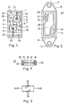
- Fig. 1 an actuator circuit consisting of two anti-parallel switched thyristors is shown. Copper foils 19, 20, 21 and 22 serving as conductor tracks are applied to the rectangular ceramic plate 1 in accordance with the method known from patent application P 30 36 128.5. A semiconductor tablet 5 or 6 (thyristors) is soldered with its anode side to each copper foil 20 or 21. The annular cathode contact 7 and the gate contact 8 designed as a central gate lie on the side of each semiconductor tablet 5, 6 opposite the anode side.
- the cathode contact 7 of the semiconductor tablet 5 is connected to the copper foil 21 and thus to the anode of the semiconductor tablet 6 via a connecting lug 9.
- the connecting lug 9 is soldered on the one hand to the ring-shaped cathode contact 7, and on the other hand to the copper foil 21.
- the cathode contact 7 of the semiconductor tablet 6 is connected to the copper foil 20 via a connecting tab 9.
- Anode-cathode connecting wires 25 and 26 are soldered to the copper foils 20 and 21.
- the connecting wires 25 and 26 each have a thickened foot part to increase the stability of the solder joint.
- the central gate contact 8 of the semiconductor tablet 5 is connected to the copper foil 19 via a gate connecting lug 23, both ends of the lug 23 being soldered.
- the frame 27 has a circumferential, wide, rectangular cross-section edge 28, to which a narrow, circumferential rib 29 is formed toward the inside of the frame so that the edge-rib arrangement is T-shaped in cross section.
- Two support struts 30 are molded onto the inner circumferential rib 29 in such a way that elongate openings 31 for inserting the connecting wires 24, 25, 26 each result between the inner rib 29 and the support strut 30.
- the open interior of the housing delimited by the frame is designated 32.
- the frame 27 can be provided on its two narrow sides with integrally formed connecting lugs 16, with bores 17 being provided in the lugs 16 for rivet or screw fastening on a heat sink or a metal base plate.
- FIG. 7 shows a section through the frame 27. This shows the rectangular cross section of the peripheral edge 28 and the molded inner peripheral rib 29. Between the support strut 30 and the rib 29 there is on the one hand the opening 31 for the passage of the wires 24 and 25 and on the other hand the open housing interior 32.
- the housing thus created is cast with casting resin 18, and a finished converter module is produced, as shown in FIG. 4.
- the space requirement and in particular the overall height of the module are advantageously very small.
- the connecting wires 24, 25 led out upwards and 26 are suitable for easy soldering on printed circuit boards.
- the module shown in FIG. 4 can optionally also be provided with the connecting straps 16 of FIGS. 2 or 6 for attachment to a heat sink or a metal base plate; for a circuit board monday alone these tabs 16 are not necessary, however, since the converter arrangement is then mounted only by soldering the connecting wires;
- FIG. 3 shows the electrical circuit diagram for the converter arrangement according to FIGS. 1 and 2, the reference leads 24 denoting the gate connecting wires and 25 and 26 the anode-cathode connecting wires.
- the antiparallel thyristors are designated 5 and 6.
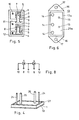
- FIG. 5 shows a thyristor branch pair as a further exemplary embodiment.
- three copper foils 2, 3, 4 serving as conductor tracks are applied to the ceramic plate 1.
- the semiconductor tablet 5 is soldered with its anode side onto the copper foil 2.
- the annular cathode contact 7 of the semiconductor tablet 5 is connected to the copper foil 3 via the connecting tab 9. connected, both ends of the tab 9 being soldered.
- the semiconductor tablet 6 is soldered to the copper foil 3 with the anode and thereby connected to the cathode of the semiconductor tablet 5.
- the annular cathode contact 7 of the tablet 6 is soldered to the copper foil 4 via a connecting flange 9.
- a head wire as an external control connection is soldered directly onto each of the gate contacts 8.
- a plastic frame 13 according to FIG. 5 is placed on the ceramic plate 1 equipped in this way and glued to the plate 1.
- the frame 13 has a peripheral edge 13a with a rectangular cross section and corresponds in length and width exactly to the ceramic plate dimensions.
- Rib 29 and support strut 30 of FIG. 2 are formed here as a uniform plate 29a, which has three bores 14 for carrying out the main connecting wires 10, 11, 12 and two bores 15 for carrying out the control connecting wires 8.
- the converter arrangement can optionally be designed both with an open ceramic plate 1 as a cooling surface and with a metal base plate.
- the connecting straps 16 can be integrally formed on the two narrow sides of the frame 13. These connection tabs 16 each have a bore 17. With the help of the tabs 16, e.g. an aluminum plate can be riveted under the ceramic plate.
- FIGS. 5 and 6 show the electrical circuit diagram associated with the thyristor branch pair according to FIGS. 5 and 6. This shows the anti-parallel connection of the semiconductor tablets 5, 6 (thyristors) with the two anode-cathode connections 10, 11 and 12 'as common connection points and the gate connections 8.
- thyristor-diode pair can alternatively be equipped with two diodes or with one diode and one thyristor (thyristor-diode pair).
Landscapes
- Rectifiers (AREA)
- Power Conversion In General (AREA)
- Input Circuits Of Receivers And Coupling Of Receivers And Audio Equipment (AREA)
- Thermistors And Varistors (AREA)
Priority Applications (1)
| Application Number | Priority Date | Filing Date | Title |
|---|---|---|---|
| AT82105679T ATE27078T1 (de) | 1981-07-11 | 1982-06-26 | Stromrichteranordnung. |
Applications Claiming Priority (2)
| Application Number | Priority Date | Filing Date | Title |
|---|---|---|---|
| DE3127456 | 1981-07-11 | ||
| DE19813127456 DE3127456A1 (de) | 1981-07-11 | 1981-07-11 | Stromrichteranordnung |
Publications (3)
| Publication Number | Publication Date |
|---|---|
| EP0069902A2 true EP0069902A2 (fr) | 1983-01-19 |
| EP0069902A3 EP0069902A3 (en) | 1984-11-28 |
| EP0069902B1 EP0069902B1 (fr) | 1987-05-06 |
Family
ID=6136699
Family Applications (1)
| Application Number | Title | Priority Date | Filing Date |
|---|---|---|---|
| EP82105679A Expired EP0069902B1 (fr) | 1981-07-11 | 1982-06-26 | Dispositif redresseur de courant |
Country Status (5)
| Country | Link |
|---|---|
| US (1) | US4488167A (fr) |
| EP (1) | EP0069902B1 (fr) |
| JP (1) | JPS5825255A (fr) |
| AT (1) | ATE27078T1 (fr) |
| DE (1) | DE3127456A1 (fr) |
Cited By (1)
| Publication number | Priority date | Publication date | Assignee | Title |
|---|---|---|---|---|
| EP0578991A1 (fr) * | 1992-07-13 | 1994-01-19 | Asea Brown Boveri Ag | Commutateur bidirectionnel semi-conducteur |
Families Citing this family (10)
| Publication number | Priority date | Publication date | Assignee | Title |
|---|---|---|---|---|
| DE3241509A1 (de) * | 1982-11-10 | 1984-05-10 | Brown, Boveri & Cie Ag, 6800 Mannheim | Leistungstransistor-modul |
| JPS59172759A (ja) * | 1983-03-22 | 1984-09-29 | Mitsubishi Electric Corp | ゲ−トタ−ンオフサイリスタモジユ−ル |
| DE3406537A1 (de) * | 1984-02-23 | 1985-08-29 | Brown, Boveri & Cie Ag, 6800 Mannheim | Anordnung eines leistungshalbleiterbauelementes auf einem isolierenden und mit leiterbahnen versehenen substrat |
| JPS6126251A (ja) * | 1984-07-16 | 1986-02-05 | Mitsubishi Electric Corp | 半導体複合素子 |
| JPS61218151A (ja) * | 1985-03-23 | 1986-09-27 | Hitachi Ltd | 半導体装置 |
| DE3538933A1 (de) * | 1985-11-02 | 1987-05-14 | Bbc Brown Boveri & Cie | Leistungshalbleitermodul |
| DE3604313A1 (de) * | 1986-02-12 | 1987-08-13 | Bbc Brown Boveri & Cie | Leistungshalbleitermodul |
| DE3604882A1 (de) * | 1986-02-15 | 1987-08-20 | Bbc Brown Boveri & Cie | Leistungshalbleitermodul und verfahren zur herstellung des moduls |
| DE3717489A1 (de) * | 1987-05-23 | 1988-12-01 | Asea Brown Boveri | Leistungshalbleitermodul und verfahren zur herstellung des moduls |
| US5391919A (en) * | 1993-10-22 | 1995-02-21 | International Rectifier Corporation | Semiconductor power module with identical mounting frames |
Family Cites Families (5)
| Publication number | Priority date | Publication date | Assignee | Title |
|---|---|---|---|---|
| JPS528427A (en) * | 1975-07-11 | 1977-01-22 | Toshiba Corp | Semiconductor rectifier |
| JPS5271625A (en) * | 1975-12-10 | 1977-06-15 | Semikron Gleichrichterbau | Semiconductor rectifier device |
| US4394530A (en) * | 1977-09-19 | 1983-07-19 | Kaufman Lance R | Power switching device having improved heat dissipation means |
| US4249034A (en) * | 1978-11-27 | 1981-02-03 | General Electric Company | Semiconductor package having strengthening and sealing upper chamber |
| US4278990A (en) * | 1979-03-19 | 1981-07-14 | General Electric Company | Low thermal resistance, low stress semiconductor package |
-
1981
- 1981-07-11 DE DE19813127456 patent/DE3127456A1/de active Granted
-
1982
- 1982-06-26 EP EP82105679A patent/EP0069902B1/fr not_active Expired
- 1982-06-26 AT AT82105679T patent/ATE27078T1/de active
- 1982-07-09 US US06/396,655 patent/US4488167A/en not_active Expired - Fee Related
- 1982-07-10 JP JP57119198A patent/JPS5825255A/ja active Pending
Cited By (1)
| Publication number | Priority date | Publication date | Assignee | Title |
|---|---|---|---|---|
| EP0578991A1 (fr) * | 1992-07-13 | 1994-01-19 | Asea Brown Boveri Ag | Commutateur bidirectionnel semi-conducteur |
Also Published As
| Publication number | Publication date |
|---|---|
| DE3127456C2 (fr) | 1988-06-16 |
| EP0069902B1 (fr) | 1987-05-06 |
| DE3127456A1 (de) | 1983-02-03 |
| ATE27078T1 (de) | 1987-05-15 |
| EP0069902A3 (en) | 1984-11-28 |
| JPS5825255A (ja) | 1983-02-15 |
| US4488167A (en) | 1984-12-11 |
Similar Documents
| Publication | Publication Date | Title |
|---|---|---|
| DE10221891C5 (de) | Leistungshalbleitervorrichtung | |
| DE69635440T2 (de) | Halbleiteranordnung mit einem Schaltungssubstrat und einem Gehäuse | |
| DE69326318T2 (de) | Verpackung für elektronische komponenten | |
| DE69637488T2 (de) | Halbleiter und Halbleitermodul | |
| DE69304304T2 (de) | Kombination einer elektronischen Halbleiteranordnung und einer Wärmesenke | |
| DE4323827C1 (de) | Steckbare Baugruppe | |
| DE102005024900B4 (de) | Leistungsmodul | |
| DE7512573U (de) | Halbleitergleichrichteranordnung | |
| DE3406528A1 (de) | Leistungshalbleitermodul | |
| DE2556749A1 (de) | Leistungshalbleiterbauelement in scheibenzellenbauweise | |
| DE2337694A1 (de) | Halbleitergleichrichteranordnung | |
| DE10313917A1 (de) | Halbleitervorrichtung | |
| EP3095307B1 (fr) | Circuit imprimé, montage et procédé de fabrication d'un montage | |
| DE1937664B2 (de) | Halbleiterbauelement | |
| DE4004737A1 (de) | Elektronische baueinheit mit elektrisch isolierter waermeableitung | |
| EP0069902B1 (fr) | Dispositif redresseur de courant | |
| EP0292848A2 (fr) | Module de puissance à semi-conducteur et son procédé de fabrication | |
| DE19748286A1 (de) | Elektrischer Anschlußkasten | |
| DE102004021054A1 (de) | Halbleiterbauelement | |
| DE102021110251A1 (de) | Leistungshalbleiteranordnung und wechselrichterbrücke mit leistungshalbleiteranordnung | |
| DE2306288C2 (de) | Träger für einen integrierten Schaltkreis | |
| DE2638909A1 (de) | Halbleiteranordnung | |
| EP0086483B1 (fr) | Arrangement de redresseur de puissance | |
| DE102021209438A1 (de) | Leistungshalbleiterbauteil und Verfahren zur Herstellung eines Leistungshalbleiterbauteils | |
| DE3628556C1 (en) | Semiconductor device |
Legal Events
| Date | Code | Title | Description |
|---|---|---|---|
| PUAI | Public reference made under article 153(3) epc to a published international application that has entered the european phase |
Free format text: ORIGINAL CODE: 0009012 |
|
| AK | Designated contracting states |
Designated state(s): AT BE CH FR GB IT LI NL SE |
|
| PUAL | Search report despatched |
Free format text: ORIGINAL CODE: 0009013 |
|
| AK | Designated contracting states |
Designated state(s): AT BE CH FR GB IT LI NL SE |
|
| 17P | Request for examination filed |
Effective date: 19841214 |
|
| 17Q | First examination report despatched |
Effective date: 19860213 |
|
| GRAA | (expected) grant |
Free format text: ORIGINAL CODE: 0009210 |
|
| AK | Designated contracting states |
Kind code of ref document: B1 Designated state(s): AT BE CH FR GB IT LI NL SE |
|
| REF | Corresponds to: |
Ref document number: 27078 Country of ref document: AT Date of ref document: 19870515 Kind code of ref document: T |
|
| ITF | It: translation for a ep patent filed | ||
| ET | Fr: translation filed | ||
| PLBE | No opposition filed within time limit |
Free format text: ORIGINAL CODE: 0009261 |
|
| STAA | Information on the status of an ep patent application or granted ep patent |
Free format text: STATUS: NO OPPOSITION FILED WITHIN TIME LIMIT |
|
| 26N | No opposition filed | ||
| PGFP | Annual fee paid to national office [announced via postgrant information from national office to epo] |
Ref country code: AT Payment date: 19900425 Year of fee payment: 9 |
|
| PGFP | Annual fee paid to national office [announced via postgrant information from national office to epo] |
Ref country code: SE Payment date: 19900525 Year of fee payment: 9 Ref country code: CH Payment date: 19900525 Year of fee payment: 9 |
|
| PGFP | Annual fee paid to national office [announced via postgrant information from national office to epo] |
Ref country code: BE Payment date: 19900612 Year of fee payment: 9 |
|
| PGFP | Annual fee paid to national office [announced via postgrant information from national office to epo] |
Ref country code: NL Payment date: 19900630 Year of fee payment: 9 |
|
| PGFP | Annual fee paid to national office [announced via postgrant information from national office to epo] |
Ref country code: FR Payment date: 19910503 Year of fee payment: 10 |
|
| PGFP | Annual fee paid to national office [announced via postgrant information from national office to epo] |
Ref country code: GB Payment date: 19910515 Year of fee payment: 10 |
|
| PG25 | Lapsed in a contracting state [announced via postgrant information from national office to epo] |
Ref country code: AT Effective date: 19910626 |
|
| PG25 | Lapsed in a contracting state [announced via postgrant information from national office to epo] |
Ref country code: SE Effective date: 19910627 |
|
| ITTA | It: last paid annual fee | ||
| PG25 | Lapsed in a contracting state [announced via postgrant information from national office to epo] |
Ref country code: LI Effective date: 19910630 Ref country code: CH Effective date: 19910630 Ref country code: BE Effective date: 19910630 |
|
| BERE | Be: lapsed |
Owner name: BROWN BOVERI & CIE A.G. Effective date: 19910630 |
|
| PG25 | Lapsed in a contracting state [announced via postgrant information from national office to epo] |
Ref country code: NL Effective date: 19920101 |
|
| NLV4 | Nl: lapsed or anulled due to non-payment of the annual fee | ||
| REG | Reference to a national code |
Ref country code: CH Ref legal event code: PL |
|
| PG25 | Lapsed in a contracting state [announced via postgrant information from national office to epo] |
Ref country code: GB Effective date: 19920626 |
|
| GBPC | Gb: european patent ceased through non-payment of renewal fee |
Effective date: 19920626 |
|
| PG25 | Lapsed in a contracting state [announced via postgrant information from national office to epo] |
Ref country code: FR Effective date: 19930226 |
|
| REG | Reference to a national code |
Ref country code: FR Ref legal event code: ST |
|
| EUG | Se: european patent has lapsed |
Ref document number: 82105679.3 Effective date: 19920109 |