EP0069902A2 - Current rectifier device - Google Patents
Current rectifier device Download PDFInfo
- Publication number
- EP0069902A2 EP0069902A2 EP82105679A EP82105679A EP0069902A2 EP 0069902 A2 EP0069902 A2 EP 0069902A2 EP 82105679 A EP82105679 A EP 82105679A EP 82105679 A EP82105679 A EP 82105679A EP 0069902 A2 EP0069902 A2 EP 0069902A2
- Authority
- EP
- European Patent Office
- Prior art keywords
- frame
- ceramic plate
- housing
- converter
- circumferential rib
- Prior art date
- Legal status (The legal status is an assumption and is not a legal conclusion. Google has not performed a legal analysis and makes no representation as to the accuracy of the status listed.)
- Granted
Links
Images
Classifications
-
- H—ELECTRICITY
- H10—SEMICONDUCTOR DEVICES; ELECTRIC SOLID-STATE DEVICES NOT OTHERWISE PROVIDED FOR
- H10W—GENERIC PACKAGES, INTERCONNECTIONS, CONNECTORS OR OTHER CONSTRUCTIONAL DETAILS OF DEVICES COVERED BY CLASS H10
- H10W76/00—Containers; Fillings or auxiliary members therefor; Seals
- H10W76/10—Containers or parts thereof
- H10W76/12—Containers or parts thereof characterised by their shape
- H10W76/15—Containers comprising an insulating or insulated base
-
- H—ELECTRICITY
- H10—SEMICONDUCTOR DEVICES; ELECTRIC SOLID-STATE DEVICES NOT OTHERWISE PROVIDED FOR
- H10W—GENERIC PACKAGES, INTERCONNECTIONS, CONNECTORS OR OTHER CONSTRUCTIONAL DETAILS OF DEVICES COVERED BY CLASS H10
- H10W90/00—Package configurations
Definitions
- the invention relates to a converter arrangement with a cuboid housing cast with a hardened insulating material and with a ceramic plate which is provided with conductor tracks made of copper foil on the surface facing the interior of the housing, onto which semiconductor tablets are soldered, the semiconductor tablets being connected to one another by connecting straps and connection elements of the converter arrangement on the top, the housing are freely accessible.
- Potted converter sets also known as modules, are generally known.
- the encapsulation effort is too great, ie the installation of the less powerful circuit in a device provided for a more powerful circuit Housing leads to unnecessarily high material and assembly costs during production and the user must provide unnecessarily large assembly areas.
- the object of the invention is to create a converter arrangement for branch pair circuits with currents less than 25 A, the dimensions of which, in particular the housing height, are as small as possible and which is also particularly suitable for direct circuit board installation.
- the converter arrangement has a low thermal resistance between the active part and the outer housing surface due to the use of the ceramic plate.
- the assembly and encapsulation effort of the arrangement is advantageously low.
- the user only has to provide small mounting surfaces, which enables a compact design.
- the housing itself does not have the supporting function of the module, but the ceramic plate.
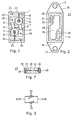
- Fig. 1 an actuator circuit consisting of two anti-parallel switched thyristors is shown. Copper foils 19, 20, 21 and 22 serving as conductor tracks are applied to the rectangular ceramic plate 1 in accordance with the method known from patent application P 30 36 128.5. A semiconductor tablet 5 or 6 (thyristors) is soldered with its anode side to each copper foil 20 or 21. The annular cathode contact 7 and the gate contact 8 designed as a central gate lie on the side of each semiconductor tablet 5, 6 opposite the anode side.
- the cathode contact 7 of the semiconductor tablet 5 is connected to the copper foil 21 and thus to the anode of the semiconductor tablet 6 via a connecting lug 9.
- the connecting lug 9 is soldered on the one hand to the ring-shaped cathode contact 7, and on the other hand to the copper foil 21.
- the cathode contact 7 of the semiconductor tablet 6 is connected to the copper foil 20 via a connecting tab 9.
- Anode-cathode connecting wires 25 and 26 are soldered to the copper foils 20 and 21.
- the connecting wires 25 and 26 each have a thickened foot part to increase the stability of the solder joint.
- the central gate contact 8 of the semiconductor tablet 5 is connected to the copper foil 19 via a gate connecting lug 23, both ends of the lug 23 being soldered.
- the frame 27 has a circumferential, wide, rectangular cross-section edge 28, to which a narrow, circumferential rib 29 is formed toward the inside of the frame so that the edge-rib arrangement is T-shaped in cross section.
- Two support struts 30 are molded onto the inner circumferential rib 29 in such a way that elongate openings 31 for inserting the connecting wires 24, 25, 26 each result between the inner rib 29 and the support strut 30.
- the open interior of the housing delimited by the frame is designated 32.
- the frame 27 can be provided on its two narrow sides with integrally formed connecting lugs 16, with bores 17 being provided in the lugs 16 for rivet or screw fastening on a heat sink or a metal base plate.
- FIG. 7 shows a section through the frame 27. This shows the rectangular cross section of the peripheral edge 28 and the molded inner peripheral rib 29. Between the support strut 30 and the rib 29 there is on the one hand the opening 31 for the passage of the wires 24 and 25 and on the other hand the open housing interior 32.
- the housing thus created is cast with casting resin 18, and a finished converter module is produced, as shown in FIG. 4.
- the space requirement and in particular the overall height of the module are advantageously very small.
- the connecting wires 24, 25 led out upwards and 26 are suitable for easy soldering on printed circuit boards.
- the module shown in FIG. 4 can optionally also be provided with the connecting straps 16 of FIGS. 2 or 6 for attachment to a heat sink or a metal base plate; for a circuit board monday alone these tabs 16 are not necessary, however, since the converter arrangement is then mounted only by soldering the connecting wires;
- FIG. 3 shows the electrical circuit diagram for the converter arrangement according to FIGS. 1 and 2, the reference leads 24 denoting the gate connecting wires and 25 and 26 the anode-cathode connecting wires.
- the antiparallel thyristors are designated 5 and 6.
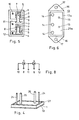
- FIG. 5 shows a thyristor branch pair as a further exemplary embodiment.
- three copper foils 2, 3, 4 serving as conductor tracks are applied to the ceramic plate 1.
- the semiconductor tablet 5 is soldered with its anode side onto the copper foil 2.
- the annular cathode contact 7 of the semiconductor tablet 5 is connected to the copper foil 3 via the connecting tab 9. connected, both ends of the tab 9 being soldered.
- the semiconductor tablet 6 is soldered to the copper foil 3 with the anode and thereby connected to the cathode of the semiconductor tablet 5.
- the annular cathode contact 7 of the tablet 6 is soldered to the copper foil 4 via a connecting flange 9.
- a head wire as an external control connection is soldered directly onto each of the gate contacts 8.
- a plastic frame 13 according to FIG. 5 is placed on the ceramic plate 1 equipped in this way and glued to the plate 1.
- the frame 13 has a peripheral edge 13a with a rectangular cross section and corresponds in length and width exactly to the ceramic plate dimensions.
- Rib 29 and support strut 30 of FIG. 2 are formed here as a uniform plate 29a, which has three bores 14 for carrying out the main connecting wires 10, 11, 12 and two bores 15 for carrying out the control connecting wires 8.
- the converter arrangement can optionally be designed both with an open ceramic plate 1 as a cooling surface and with a metal base plate.
- the connecting straps 16 can be integrally formed on the two narrow sides of the frame 13. These connection tabs 16 each have a bore 17. With the help of the tabs 16, e.g. an aluminum plate can be riveted under the ceramic plate.
- FIGS. 5 and 6 show the electrical circuit diagram associated with the thyristor branch pair according to FIGS. 5 and 6. This shows the anti-parallel connection of the semiconductor tablets 5, 6 (thyristors) with the two anode-cathode connections 10, 11 and 12 'as common connection points and the gate connections 8.
- thyristor-diode pair can alternatively be equipped with two diodes or with one diode and one thyristor (thyristor-diode pair).
Landscapes
- Rectifiers (AREA)
- Power Conversion In General (AREA)
- Input Circuits Of Receivers And Coupling Of Receivers And Audio Equipment (AREA)
- Thermistors And Varistors (AREA)
Abstract
Es wird eine Stromrichteranordnung angegeben, die eine mit Halbleitertabletten (5, 6) bestückte Keramikplatte (1) sowie einen daraufgesetzten und mit der Keramikplatte (1) verklebten Rahmen (27) aufweist. Der Rahmen (27) ist oben und unten offen und besteht aus einer im Querschnitt rechteckförmigen Kante (28), an die mittig und zum Rahmeninneren hin gerichtet eine schmale, umlaufende Rippe (29) angeformt ist. An die innere umlaufende Rippe (29) sind Stützstreben (30) zur Umfassung der aus dem Gehäuse geführten Anschlußdrähte (24, 25, 26) angeformt. Das fertige Gehäuse wird mit einer aushärtbaren Isolierstoffmasse aus gegossen. Das so geschaffene Stromrichtermodul eignet sich vorzugsweise für Stromstärken bis 25A und wegen seines flachen Aufbaues zum direkten Leiterplatten-Einbau.The invention relates to a converter arrangement which has a ceramic plate (1) fitted with semiconductor tablets (5, 6) and a frame (27) placed thereon and glued to the ceramic plate (1). The frame (27) is open at the top and bottom and consists of an edge (28) which is rectangular in cross section and to which a narrow, circumferential rib (29) is formed in the center and towards the inside of the frame. Support struts (30) for enclosing the connecting wires (24, 25, 26) guided out of the housing are molded onto the inner circumferential rib (29). The finished housing is cast with a curable insulating material. The converter module created in this way is particularly suitable for currents up to 25A and, due to its flat design, for direct PCB installation.
Description
Die Erfindung bezieht sich auf eine Stromrichteranordnung mit einem quaderförmigen, mit einer ausgehärteten Isolierstoffmasse ausgegossenen Gehäuse und mit einer Keramikplatte, die auf der dem Gehäuseinneren zugewandten Fläche mit Leiterbahnen aus Kupferfolie versehen ist, auf die Halbleitertabletten aufgelötet sind, wobei die Halbleitertabletten untereinander durch Verbindungslaschen verbunden sind und Anschlußelemente der Stromrichteranordnung auf der Oberseite, des Gehäuses frei zugänglich sind.The invention relates to a converter arrangement with a cuboid housing cast with a hardened insulating material and with a ceramic plate which is provided with conductor tracks made of copper foil on the surface facing the interior of the housing, onto which semiconductor tablets are soldered, the semiconductor tablets being connected to one another by connecting straps and connection elements of the converter arrangement on the top, the housing are freely accessible.
Vergossene Stromrichtersätze, auch als Module bezeichnet, sind allgemein bekannt. Für Zweigpaar-Schaltungen von Thyristoren und Dioden gibt es bereits ein international eingeführtes Gehäuse, das nach Aufbau und Größe für den Dauergrenzstrombereich zwischen 20A und 100A geeignet ist. Für Stromstärken unter 20 Ampere ist der Kapselungsaufwand jedoch zu groß, d.h. der Einbau der leistungsschwächeren Schaltung in ein für eine leistungsstärkere Schaltung vorgesehenes Gehäuse führt zu unnötig hohem Material- und Montageaufwand bei der Herstellung und der Anwender muß unnötig große Montageflächen zur Verfügung stellen.Potted converter sets, also known as modules, are generally known. There is already an internationally introduced housing for two-pair circuits of thyristors and diodes, which is suitable for the permanent limit current range between 20A and 100A. For currents below 20 amperes, however, the encapsulation effort is too great, ie the installation of the less powerful circuit in a device provided for a more powerful circuit Housing leads to unnecessarily high material and assembly costs during production and the user must provide unnecessarily large assembly areas.
Als Alternative hierzu wird in einem Prospekt der Firma Semikron Gesellschaft für Gleichrichterbau und Elektronik m.b.H., Nürnberg, "Glaspassivierte Thyristor-Tabletten, Semipack" eine Stromrichteranordnung mit einem relativ kleinen Gehäuse vorgeschlagen: Semipack 0, SKKT 15, SKKH 15, SKKD 15, SKKE 15. Selbst dieses verhältnismäßig kleine Gehäuse hat in nachteiliger Weise einen großen Platzbedarf. Es besitzt eine massive Grundplatte aus vernickeltem Kupfer. Dadurch wird zwar ein Durchbiegen der Grundplatte nach den Löt-.und Kapselungsprozessen weitgehend vermieden, das Verfahren zur Aufbringung der Grundplatte ist jedoch relativ aufwendig:As an alternative to this, a prospectus from Semikron Gesellschaft für rectifier construction and electronics mbH, Nuremberg, "Glass Passivated Thyristor Tablets, Semipack" proposes a converter arrangement with a relatively small housing: Semipack 0, SKKT 15, SKKH 15, SKKD 15, SKKE 15 Even this relatively small housing disadvantageously requires a large amount of space. It has a solid base plate made of nickel-plated copper. This will cause the base plate to bend after the soldering . and encapsulation processes largely avoided, but the process for applying the base plate is relatively complex:
Für leistungsschwächere Zweigpaarschaltungen wird von einem anderen Hersteller (MEDL/AEI) bereits ein noch kleinerer Modul angeboten: Reihe PB..... Auch bei dieser Ausführung ist die isolierte Keramik mit einer metallischen Grundplatte verlötet.Another manufacturer (MEDL / AEI) is already offering an even smaller module for lower-power branch pair circuits: Series PB ..... In this version, too, the insulated ceramic is soldered to a metallic base plate.
Der Erfindung liegt davon ausgehend die Aufgabe zugrunde, eine Stromrichteranordnung für Zweigpaarschaltungen mit Stromstärken kleiner als 25 A zu schaffen, deren Abmessungen, insbesondere die Gehäusehöhe, möglichst gering sind und die sich insbesondere auch für einen direkten Leiterplatten-Einbau eignet.Proceeding from this, the object of the invention is to create a converter arrangement for branch pair circuits with currents less than 25 A, the dimensions of which, in particular the housing height, are as small as possible and which is also particularly suitable for direct circuit board installation.
Diese Aufgabe wird erfindungsgemäß durch eine Stromrichteranordnung der eingangs genannten Art mit folgenden Merkmalen gelöst:
- - das Gehäuse besteht aus einem flachen, oben und unten offenen Rahmen, dessen Länge und Breite genau den Außenabmessungen der Keramikplatte entsprechen,
- - der Rahmen weist eine umlaufende, im Querschnitt rechteckförmige Kante auf, an die mittig und zum Rahmeninneren hin gerichtet eine schmale, umlaufende Rippe angeformt ist,
- - an die innere umlaufende Rippe sind Stützstreben zur Umfassung der aus dem Gehäuse geführten Anschlußelemente angeformt,
- - die Verbindung Keramikplatte-Rahmen ist geklebt,
- - die Anschlußelemente - Drähte oder Flachstecker - sind .senkrecht zur Keramikplatte herausgeführt....
- - the housing consists of a flat frame, open at the top and bottom, the length and width of which correspond exactly to the outer dimensions of the ceramic plate,
- the frame has a circumferential edge which is rectangular in cross section and to which a narrow circumferential rib is formed in the center and towards the interior of the frame,
- - Support struts are formed on the inner circumferential rib to enclose the connection elements led out of the housing,
- - the connection between the ceramic plate and the frame is glued,
- - The connection elements - wires or flat plugs - are led out perpendicular to the ceramic plate ....
Die mit der Erfindung erzielbaren Vorteile liegen insbesondere darin, daß die Stromrichteranordnung durch den Einsatz der Keramikplatte einen geringen Wärmewiderstand zwischen Aktivteil und Gehäuseaußenfläche aufweist. Der Montage- und Kapselungsaufwand der Anordnung ist vorteilhaft gering. Der Anwender muß nur geringe Montageflächen zur Verfügung-stellen, was eine kompakte Bauweise ermöglicht. Im Gegensatz zu bekannten Stromrichteranordnungen hat nicht das Gehäuse selbst die tragende Funktion des Moduls, sondern die Keramikplatte.The advantages that can be achieved with the invention are, in particular, that the converter arrangement has a low thermal resistance between the active part and the outer housing surface due to the use of the ceramic plate. The assembly and encapsulation effort of the arrangement is advantageously low. The user only has to provide small mounting surfaces, which enables a compact design. In contrast to known converter arrangements, the housing itself does not have the supporting function of the module, but the ceramic plate.
Ausführungsbeispiele der Erfindung sind nachfolgend anhand der Zeichnungen erläutert.Embodiments of the invention are explained below with reference to the drawings.
Es zeigen:
- Fig. 1 eine Stellerschaltung aus zwei antiparallel ge- schalteten. Thyristoren,
- Fig. 2 einen Kunststoffrahmen hierzu,
- Fig. 3 das elektrische Schaltbild zur Stellerschaltung,
- Fig. 4 das vergossene Stromrichtermodul,
- Fig. 5 ein Thyristor-Zweigpaar,
- Fig. 6 einen Kunststoffrahmen hierzu,
- Fig. 7 einen Schnitt durch den Rahmen,
- Fig. 8 das elektrische Schaltbild zum Zweigpaar.
- 1 shows an actuator circuit consisting of two connected in anti-parallel. Thyristors,
- 2 a plastic frame for this purpose,
- 3 shows the electrical circuit diagram for the actuator circuit,
- 4 the encapsulated converter module,
- 5 shows a pair of thyristor branches,
- 6 shows a plastic frame for this purpose,
- 7 shows a section through the frame,
- Fig. 8 shows the electrical circuit diagram for the pair of branches.
In Fig. 1 ist eine Stellerschaltung, bestehend aus zwei antiparallei geschalteten Thyristoren dargestellt. Auf der rechteckförmigen Keramikplatte 1 sind als Leiterbahnen dienende Kupferfolien 19, 20, 21 und 22 gemäß dem aus Patentanmeldung P 30 36 128.5 bekannten Verfahren aufgebracht. Auf jeder Kupferfolie 20 bzw. 21 ist jeweils eine Halbleitertablette 5 bzw. 6 (Thyristoren) mit ihrer Anodenseite gelötet. Der ringförmige Kathodenkontakt 7 und der als Zentralgate ausgebildete Gatekontakt 8 liegen auf der der Anodenseite gegenüberliegenden Seite jeder Halbleitertablette 5, 6.In Fig. 1, an actuator circuit consisting of two anti-parallel switched thyristors is shown.
Der Kathodenkontakt 7 der Halbleitertablette 5 ist über eine Verbindungslasche 9 mit der Kupferfolie 21 und damit mit der Anode der Halbleitertablette 6 verbunden. Die Verbindungslasche 9 ist dabei einerseits mit dem ringförmigen Kathodenkontakt-7, andererseits mit der Kupferfolie 21 verlötet. Auf gleiche Weise ist der Kathodenkontakt 7 der Halbleitertablette 6 über eine Verbindungslasche 9 mit der Kupferfolie 20 verbunden. Auf die Kupferfolien 20 und 21 sind Anoden-Kathoden-Anschlußdrähte 25 und 26 gelötet. Die Anschlußdrähte 25 und 26 weisen jeweils ein verdicktes Fußteil zur Erhöhung der Stabilität der Lötstelle auf.The cathode contact 7 of the
Der zentrale Gatekontakt 8 der Halbleitertablette 5 ist über eine Gate-Verbindungslasche 23 mit der Kupferfolie 19 verbunden, wobei beide Enden der Lasche 23 verlötet sind. Auf der Kupferfolie 19 ist ferner ein Anschlußdraht 24 für den externen Gateanschluß verlötet.The
In Fig. 2 ist der Kunststoffrahmen 27 für die bestückte Keramikplatte 1 gemäß Fig. 1 dargestellt. Der Rahmen 27 weist eine umlaufende, breite, im Querschnitt rechteckige Kante 28 auf, an die zum Rahmeninneren hin eine schmale, umlaufende Rippe 29 so angeformt ist, daß die Kanten-Rippen-Anordnung im Querschnitt T-förmig ist. An die innere umlaufende Rippe 29 sind zwei Stützstreben 30 so angeformt, daß sich zwischen innerer Rippe 29 und Stützstrebe 30 jeweils längliche Öffnungen 31 zum Durchstecken der Anschlußdrähte 24, 25, 26 ergeben. Das offene, durch den Rahmen begrenzte Gehäuseinnere ist mit 32 bezeichnet.2 shows the
Der Rahmen 27 kann an seinen beiden Schmalseiten mit angeformten Anschlußlaschen 16 versehen sein, wobei in den Laschen 16 Bohrungen 17 zur Niet- bzw. Schraubbefestigung auf einem Kühlkörper bzw. einer Metallgrundplatte vorgesehen sind.The
In Fig. 7 ist ein Schnitt durch den Rahmen 27 dargestellt. Daraus sind der rechteckförmige Querschnitt der umlaufenden Kante 28 sowie die angeformte innere umlaufende Rippe 29 ersichtlich. Zwischen Stützstrebe 30 und Rippe 29 befindet sich einerseits die Öffnung 31 zur Durchführung der Drähte 24 und 25, andererseits das offene Gehäuseinnere 32.7 shows a section through the
Nach dem Verkleben des Kunststoffrahmens 27 mit der bestückten Keramikplatte 1 wird das so geschaffene Gehäuse mit Gießharz 18 vergossen, und es entsteht ein fertiges Stromrichtermodul wie in Fig. 4 dargestellt. Der Platzbedarf und insbesondere die Bauhöhe des Moduls sind vorteilhaft sehr gering. Die nach oben herausgeführten Anschlußdrähte 24, 25 und 26 eignen sich zum leichten Verlöten auf gedruckten Schaltplatinen.After the
Das in Fig. 4 abgebildete Modul kann wahlweise noch mit den Anschlußlaschen 16 der Fig. 2 oder 6 zur Befestigung auf einem Kühlkörper oder einer Metallgrundplatte versehen sein; für eine Leiterplattenmöntage allein sind diese Laschen 16 jedoch nicht nötigt, da dann die Stromrichteranordnung lediglich durch Verlöten der Anschlußdrähte montiert wird;The module shown in FIG. 4 can optionally also be provided with the connecting
In Fig. 3 ist das elektrische Schaltbild zur Stromrichteranordnung gemäß den Figuren 1 und 2 dargestellt, wobei mit Bezugszeichen 24 die Gate-Anschlußdrähte, mit 25 und 26 die Anoden-Kathoden-Anschlußdrähte bezeichnet sind. Die antiparallel liegenden Thyristoren sind mit 5 und 6 bezeichnet.3 shows the electrical circuit diagram for the converter arrangement according to FIGS. 1 and 2, the reference leads 24 denoting the gate connecting wires and 25 and 26 the anode-cathode connecting wires. The antiparallel thyristors are designated 5 and 6.
In Fig. 5 ist als weiteres Ausführungsbeispiel ein Thyristor-Zweigpaar dargestellt. Auf der Keramikplatte 1 sind dabei drei als Leiterbahnen dienende Kupferfolien 2, 3, 4 aufgebracht. Auf die Kupferfolie 2 ist die Halbleitertablette 5 mit ihrer Anodenseite aufgelötet.5 shows a thyristor branch pair as a further exemplary embodiment. In this case, three copper foils 2, 3, 4 serving as conductor tracks are applied to the
Der ringförmige Kathodenkontakt 7 der Halbleitertablette 5 ist über die Verbindungslasche 9 mit der Kupferfolie 3 . verbunden, wobei beide Enden der Lasche 9 verlötet sind. Auf die Kupferfolie 3 ist die Halbleitertablette 6 mit der Anode gelötet und dadurch mit der Kathode der Halbleitertablette 5 verbunden. Der ringförmige Kathodenkontakt 7 der Tablette 6 ist über eine Verbindungslansche 9 mit der Kupferfolie 4 verlötet.The
Auf die Kupferfolien 2, 3 und 4 sind externe Anschlußdrähte 10, 11 und 12 aufgelötet.External leads 10, 11 and 12 are soldered onto the copper foils 2, 3 and 4.
Auf jedem der Gatekontakte 8 ist ein Kopfdraht als externer Steueranschluß direkt aufgelötet.A head wire as an external control connection is soldered directly onto each of the
Auf die so bestückte Keramikplate 1 wird ein Kunststoffrahmen 13 gemäß Fig. 5 aufgelegt und mit der Platte 1.verklebt. Der Rahmen 13 besitzt eine umlaufende Kante 13a mit rechteckförmigem Querschnitt und entspricht in seiner Länge und Breite dabei genau den Keramikplattenabmessungen. Rippe 29 und Stützstrebe 30 der Fig. 2 sind hier als einheitliche Platte 29a ausgebildet, die zur Durchführung der Hauptanschlußdrähte 10, 11, 12 drei Bohrungen 14 sowie zur Durchführung der Steueranschlußdrähte 8 zwei Bohrungen 15 aufweist.A
Die Stromrichteranordnung kann wahlweise sowohl mit offener Keramikplatte 1 als Kühlfläche ausgeführt werden, als auch mit einer Metallgrundplatte. Zur Befestigung der Metallgrundplatte können an die beiden Schmalseiten des Rahmens 13 wieder die Anschlußlaschen 16 angeformt sein. Diese Anschlußlaschen 16 weisen jeweilseine Bohrung 17 auf. Mit Hilfe der Laschen 16 kann z.B. eine Aluminiumplatte unter die Keramikplatte 1. genietet werden.The converter arrangement can optionally be designed both with an open
In Fig. 8 ist das zum Thyristor-Zweigpaar gemäß den Figuren 5 und 6 zugehörige elektrische Schaltbild dargestellt. Daraus ist die Antiparallelschaltung der Halbleitertabletten 5, 6 (Thyristoren) mit den beiden Anoden-Kathoden-Anschlüssen 10, 11 und 12'als gemeinsame Anschlußpunkte sowie den Gate-Anschlüssen 8 ersichtlich.8 shows the electrical circuit diagram associated with the thyristor branch pair according to FIGS. 5 and 6. This shows the anti-parallel connection of the
Die Stromrichteranordnung gemäß Fig. 5 kann alternativ auch mit zwei Dioden oder mit jeweils einer Diode und einem Thyristor (Thyristor-Diode-Zweigpaar) bestückt werden.5 can alternatively be equipped with two diodes or with one diode and one thyristor (thyristor-diode pair).
Claims (3)
Priority Applications (1)
| Application Number | Priority Date | Filing Date | Title |
|---|---|---|---|
| AT82105679T ATE27078T1 (en) | 1981-07-11 | 1982-06-26 | POWER CONVERTER ARRANGEMENT. |
Applications Claiming Priority (2)
| Application Number | Priority Date | Filing Date | Title |
|---|---|---|---|
| DE3127456 | 1981-07-11 | ||
| DE19813127456 DE3127456A1 (en) | 1981-07-11 | 1981-07-11 | RECTIFIER ARRANGEMENT |
Publications (3)
| Publication Number | Publication Date |
|---|---|
| EP0069902A2 true EP0069902A2 (en) | 1983-01-19 |
| EP0069902A3 EP0069902A3 (en) | 1984-11-28 |
| EP0069902B1 EP0069902B1 (en) | 1987-05-06 |
Family
ID=6136699
Family Applications (1)
| Application Number | Title | Priority Date | Filing Date |
|---|---|---|---|
| EP82105679A Expired EP0069902B1 (en) | 1981-07-11 | 1982-06-26 | Current rectifier device |
Country Status (5)
| Country | Link |
|---|---|
| US (1) | US4488167A (en) |
| EP (1) | EP0069902B1 (en) |
| JP (1) | JPS5825255A (en) |
| AT (1) | ATE27078T1 (en) |
| DE (1) | DE3127456A1 (en) |
Cited By (1)
| Publication number | Priority date | Publication date | Assignee | Title |
|---|---|---|---|---|
| EP0578991A1 (en) * | 1992-07-13 | 1994-01-19 | Asea Brown Boveri Ag | Bidirectional semiconductor switch |
Families Citing this family (10)
| Publication number | Priority date | Publication date | Assignee | Title |
|---|---|---|---|---|
| DE3241509A1 (en) * | 1982-11-10 | 1984-05-10 | Brown, Boveri & Cie Ag, 6800 Mannheim | POWER TRANSISTOR MODULE |
| JPS59172759A (en) * | 1983-03-22 | 1984-09-29 | Mitsubishi Electric Corp | Gate turn off thyristor module |
| DE3406537A1 (en) * | 1984-02-23 | 1985-08-29 | Brown, Boveri & Cie Ag, 6800 Mannheim | ARRANGEMENT OF A PERFORMANCE SEMICONDUCTOR COMPONENT ON AN INSULATING AND PROVIDED SUBSTRATE |
| JPS6126251A (en) * | 1984-07-16 | 1986-02-05 | Mitsubishi Electric Corp | Semiconductor composite element |
| JPS61218151A (en) * | 1985-03-23 | 1986-09-27 | Hitachi Ltd | Semiconductor device |
| DE3538933A1 (en) * | 1985-11-02 | 1987-05-14 | Bbc Brown Boveri & Cie | PERFORMANCE SEMICONDUCTOR MODULE |
| DE3604313A1 (en) * | 1986-02-12 | 1987-08-13 | Bbc Brown Boveri & Cie | PERFORMANCE SEMICONDUCTOR MODULE |
| DE3604882A1 (en) * | 1986-02-15 | 1987-08-20 | Bbc Brown Boveri & Cie | PERFORMANCE SEMICONDUCTOR MODULE AND METHOD FOR PRODUCING THE MODULE |
| DE3717489A1 (en) * | 1987-05-23 | 1988-12-01 | Asea Brown Boveri | PERFORMANCE SEMICONDUCTOR MODULE AND METHOD FOR PRODUCING THE MODULE |
| US5391919A (en) * | 1993-10-22 | 1995-02-21 | International Rectifier Corporation | Semiconductor power module with identical mounting frames |
Family Cites Families (5)
| Publication number | Priority date | Publication date | Assignee | Title |
|---|---|---|---|---|
| JPS528427A (en) * | 1975-07-11 | 1977-01-22 | Toshiba Corp | Semiconductor rectifier |
| JPS5271625A (en) * | 1975-12-10 | 1977-06-15 | Semikron Gleichrichterbau | Semiconductor rectifier device |
| US4394530A (en) * | 1977-09-19 | 1983-07-19 | Kaufman Lance R | Power switching device having improved heat dissipation means |
| US4249034A (en) * | 1978-11-27 | 1981-02-03 | General Electric Company | Semiconductor package having strengthening and sealing upper chamber |
| US4278990A (en) * | 1979-03-19 | 1981-07-14 | General Electric Company | Low thermal resistance, low stress semiconductor package |
-
1981
- 1981-07-11 DE DE19813127456 patent/DE3127456A1/en active Granted
-
1982
- 1982-06-26 EP EP82105679A patent/EP0069902B1/en not_active Expired
- 1982-06-26 AT AT82105679T patent/ATE27078T1/en active
- 1982-07-09 US US06/396,655 patent/US4488167A/en not_active Expired - Fee Related
- 1982-07-10 JP JP57119198A patent/JPS5825255A/en active Pending
Cited By (1)
| Publication number | Priority date | Publication date | Assignee | Title |
|---|---|---|---|---|
| EP0578991A1 (en) * | 1992-07-13 | 1994-01-19 | Asea Brown Boveri Ag | Bidirectional semiconductor switch |
Also Published As
| Publication number | Publication date |
|---|---|
| DE3127456C2 (en) | 1988-06-16 |
| EP0069902B1 (en) | 1987-05-06 |
| DE3127456A1 (en) | 1983-02-03 |
| ATE27078T1 (en) | 1987-05-15 |
| EP0069902A3 (en) | 1984-11-28 |
| JPS5825255A (en) | 1983-02-15 |
| US4488167A (en) | 1984-12-11 |
Similar Documents
| Publication | Publication Date | Title |
|---|---|---|
| DE10221891C5 (en) | Power semiconductor device | |
| DE69635440T2 (en) | Semiconductor device comprising a circuit substrate and a housing | |
| DE69326318T2 (en) | PACKING FOR ELECTRONIC COMPONENTS | |
| DE69637488T2 (en) | Semiconductor and semiconductor module | |
| DE69304304T2 (en) | Combination of an electronic semiconductor device and a heat sink | |
| DE4323827C1 (en) | Pluggable assembly | |
| DE102005024900B4 (en) | power module | |
| DE7512573U (en) | SEMI-CONDUCTOR RECTIFIER ARRANGEMENT | |
| DE3406528A1 (en) | PERFORMANCE SEMICONDUCTOR MODULE | |
| DE2556749A1 (en) | POWER SEMICONDUCTOR COMPONENT IN DISC CELL DESIGN | |
| DE2337694A1 (en) | SEMI-CONDUCTOR RECTIFIER ARRANGEMENT | |
| DE10313917A1 (en) | Semiconductor circuit elements are mounted in groups on insulating pads on copper baseplate and are enclosed in plastics housing and has alternating current and positive direct current terminals | |
| EP3095307B1 (en) | Printed circuit board, circuit, and method for the production of a circuit | |
| DE1937664B2 (en) | Semiconductor component | |
| DE4004737A1 (en) | ELECTRONIC UNIT WITH ELECTRICALLY INSULATED HEAT EXHAUST | |
| EP0069902B1 (en) | Current rectifier device | |
| EP0292848A2 (en) | Semiconductor power module and method of manufacturing it | |
| DE19748286A1 (en) | Electrical terminal box for vehicle | |
| DE102004021054A1 (en) | Semiconductor component for a flip-chip structure has contact layers between a semiconductor chip and a chip carrier | |
| DE102021110251A1 (en) | POWER SEMICONDUCTOR ARRANGEMENT AND INVERTER BRIDGE WITH POWER SEMICONDUCTOR ARRANGEMENT | |
| DE2306288C2 (en) | Integrated circuit carrier | |
| DE2638909A1 (en) | SEMI-CONDUCTOR ARRANGEMENT | |
| EP0086483B1 (en) | Power rectifier arrangement | |
| DE102021209438A1 (en) | Power semiconductor device and method for producing a power semiconductor device | |
| DE3628556C1 (en) | Semiconductor device |
Legal Events
| Date | Code | Title | Description |
|---|---|---|---|
| PUAI | Public reference made under article 153(3) epc to a published international application that has entered the european phase |
Free format text: ORIGINAL CODE: 0009012 |
|
| AK | Designated contracting states |
Designated state(s): AT BE CH FR GB IT LI NL SE |
|
| PUAL | Search report despatched |
Free format text: ORIGINAL CODE: 0009013 |
|
| AK | Designated contracting states |
Designated state(s): AT BE CH FR GB IT LI NL SE |
|
| 17P | Request for examination filed |
Effective date: 19841214 |
|
| 17Q | First examination report despatched |
Effective date: 19860213 |
|
| GRAA | (expected) grant |
Free format text: ORIGINAL CODE: 0009210 |
|
| AK | Designated contracting states |
Kind code of ref document: B1 Designated state(s): AT BE CH FR GB IT LI NL SE |
|
| REF | Corresponds to: |
Ref document number: 27078 Country of ref document: AT Date of ref document: 19870515 Kind code of ref document: T |
|
| ITF | It: translation for a ep patent filed | ||
| ET | Fr: translation filed | ||
| PLBE | No opposition filed within time limit |
Free format text: ORIGINAL CODE: 0009261 |
|
| STAA | Information on the status of an ep patent application or granted ep patent |
Free format text: STATUS: NO OPPOSITION FILED WITHIN TIME LIMIT |
|
| 26N | No opposition filed | ||
| PGFP | Annual fee paid to national office [announced via postgrant information from national office to epo] |
Ref country code: AT Payment date: 19900425 Year of fee payment: 9 |
|
| PGFP | Annual fee paid to national office [announced via postgrant information from national office to epo] |
Ref country code: SE Payment date: 19900525 Year of fee payment: 9 Ref country code: CH Payment date: 19900525 Year of fee payment: 9 |
|
| PGFP | Annual fee paid to national office [announced via postgrant information from national office to epo] |
Ref country code: BE Payment date: 19900612 Year of fee payment: 9 |
|
| PGFP | Annual fee paid to national office [announced via postgrant information from national office to epo] |
Ref country code: NL Payment date: 19900630 Year of fee payment: 9 |
|
| PGFP | Annual fee paid to national office [announced via postgrant information from national office to epo] |
Ref country code: FR Payment date: 19910503 Year of fee payment: 10 |
|
| PGFP | Annual fee paid to national office [announced via postgrant information from national office to epo] |
Ref country code: GB Payment date: 19910515 Year of fee payment: 10 |
|
| PG25 | Lapsed in a contracting state [announced via postgrant information from national office to epo] |
Ref country code: AT Effective date: 19910626 |
|
| PG25 | Lapsed in a contracting state [announced via postgrant information from national office to epo] |
Ref country code: SE Effective date: 19910627 |
|
| ITTA | It: last paid annual fee | ||
| PG25 | Lapsed in a contracting state [announced via postgrant information from national office to epo] |
Ref country code: LI Effective date: 19910630 Ref country code: CH Effective date: 19910630 Ref country code: BE Effective date: 19910630 |
|
| BERE | Be: lapsed |
Owner name: BROWN BOVERI & CIE A.G. Effective date: 19910630 |
|
| PG25 | Lapsed in a contracting state [announced via postgrant information from national office to epo] |
Ref country code: NL Effective date: 19920101 |
|
| NLV4 | Nl: lapsed or anulled due to non-payment of the annual fee | ||
| REG | Reference to a national code |
Ref country code: CH Ref legal event code: PL |
|
| PG25 | Lapsed in a contracting state [announced via postgrant information from national office to epo] |
Ref country code: GB Effective date: 19920626 |
|
| GBPC | Gb: european patent ceased through non-payment of renewal fee |
Effective date: 19920626 |
|
| PG25 | Lapsed in a contracting state [announced via postgrant information from national office to epo] |
Ref country code: FR Effective date: 19930226 |
|
| REG | Reference to a national code |
Ref country code: FR Ref legal event code: ST |
|
| EUG | Se: european patent has lapsed |
Ref document number: 82105679.3 Effective date: 19920109 |