EP0069061B1 - Procédé et dispositif pour l'injection de bandes de matériel - Google Patents
Procédé et dispositif pour l'injection de bandes de matériel Download PDFInfo
- Publication number
- EP0069061B1 EP0069061B1 EP82810250A EP82810250A EP0069061B1 EP 0069061 B1 EP0069061 B1 EP 0069061B1 EP 82810250 A EP82810250 A EP 82810250A EP 82810250 A EP82810250 A EP 82810250A EP 0069061 B1 EP0069061 B1 EP 0069061B1
- Authority
- EP
- European Patent Office
- Prior art keywords
- light
- web
- scanning
- receiver
- reflected
- Prior art date
- Legal status (The legal status is an assumption and is not a legal conclusion. Google has not performed a legal analysis and makes no representation as to the accuracy of the status listed.)
- Expired
Links
- 238000000034 method Methods 0.000 title claims description 40
- 239000000463 material Substances 0.000 title claims description 31
- 230000003287 optical effect Effects 0.000 claims description 7
- 239000003365 glass fiber Substances 0.000 claims description 3
- 230000005540 biological transmission Effects 0.000 claims 3
- 210000000056 organ Anatomy 0.000 claims 3
- 230000007935 neutral effect Effects 0.000 claims 1
- 230000007547 defect Effects 0.000 description 10
- 230000000694 effects Effects 0.000 description 8
- 230000010287 polarization Effects 0.000 description 6
- 230000001052 transient effect Effects 0.000 description 6
- 239000011248 coating agent Substances 0.000 description 5
- 238000000576 coating method Methods 0.000 description 5
- 238000001914 filtration Methods 0.000 description 3
- 230000006978 adaptation Effects 0.000 description 2
- 238000000149 argon plasma sintering Methods 0.000 description 2
- 238000013016 damping Methods 0.000 description 2
- 238000009792 diffusion process Methods 0.000 description 2
- 230000005855 radiation Effects 0.000 description 2
- 230000001629 suppression Effects 0.000 description 2
- YULMNMJFAZWLLN-UHFFFAOYSA-N C=C1CCCCC1 Chemical compound C=C1CCCCC1 YULMNMJFAZWLLN-UHFFFAOYSA-N 0.000 description 1
- 230000001154 acute effect Effects 0.000 description 1
- 238000004458 analytical method Methods 0.000 description 1
- 230000002238 attenuated effect Effects 0.000 description 1
- 238000005253 cladding Methods 0.000 description 1
- 230000002950 deficient Effects 0.000 description 1
- 238000007689 inspection Methods 0.000 description 1
- 239000013307 optical fiber Substances 0.000 description 1
- 229920003023 plastic Polymers 0.000 description 1
- 238000002310 reflectometry Methods 0.000 description 1
Images


Classifications
-
- G—PHYSICS
- G01—MEASURING; TESTING
- G01N—INVESTIGATING OR ANALYSING MATERIALS BY DETERMINING THEIR CHEMICAL OR PHYSICAL PROPERTIES
- G01N21/00—Investigating or analysing materials by the use of optical means, i.e. using sub-millimetre waves, infrared, visible or ultraviolet light
- G01N21/84—Systems specially adapted for particular applications
- G01N21/88—Investigating the presence of flaws or contamination
- G01N21/89—Investigating the presence of flaws or contamination in moving material, e.g. running paper or textiles
- G01N21/8901—Optical details; Scanning details
Definitions
- the invention relates to a method and a device for checking web material according to the preamble of claims 1 and 13, respectively.
- the object on which the invention is based is achieved by a method of the type described at the outset, which has the features described in the characterizing part of claim 1.
- the method preferably also has the features stated in the characterizing part of claim 2.
- Light here means not only visible but also infrared and ultraviolet light.
- the method according to the present invention is particularly suitable for scanning light-sensitive photographic web material.
- Such a web material comprises material which carries a light-sensitive layer on a transparent plastic base which is both translucent and light-scattering. Therefore, light that has passed through such a material is a diffuse or scattered light.
- This type of photographic material must be scanned for defects in the coating with non-actinic light rays, usually using infrared light.
- the coating on photographic film material also has the property of partially reflecting light. If the web material has a carrier layer made of paper, it reflects the scanning light completely. Therefore, the signals obtained when scanning photographic sheet material may be caused by either incident light or transmitted light, depending on the circumstances.
- a laser scanning beam is preferably used in the method according to the invention.
- a preferred aspect of the method according to the invention uses the fact that the web is not only translucent but also scatters or diffuses the light.
- a polarized beam strikes and passes through the web in the scan zone. Due to the light-scattering property of the web, the transmitted light is no longer strongly polarized. A portion of this light now strikes a preferably strip-like or flake-shaped polarizing element, which further attenuates the intensity of the light beam, whereupon it reaches the receiver. The degree of damping is not significantly affected by the orientation of the element. The beam remains polarized at the scanning end points beyond the two web edges, since it has not passed the web there and is attenuated by the polarizing element in accordance with its orientation.
- the signals resulting from the passage of light through the material causing the diffusion of the transmitted light can be brought into close agreement with those which correspond to the scanning end points.
- this made the system insensitive to defects in the web. While this is for larger flaws, e.g. B. large holes or the absence of the diffusion layer on an otherwise transparent carrier web, the presence of less noticeable defects leads to modify the intensity of the transmitted light without causing a significant deviation from the arbitrariness of the polarization.
- the system therefore remains sufficiently sensitive to such errors. It is common in practice to provide separate coarse defect detectors which indicate a small coating area and other gross defects. In addition, stray light is also predominantly polarized.
- the intensity of the light deflected by the light deflecting means will be greater than the intensity of the light reflected by the web; therefore, a light-attenuating filter is preferably placed in the path of the redirected light.
- the procedure is in accordance with the features of the characterizing part of claim 7, if it is a mirror, the procedure is preferably in accordance with the features described in the characterizing part of claims 8 and 9, respectively.
- the light deflecting means can also be light-guiding elements, in particular an optical fiber arrangement consisting of glass fibers, or also light-refracting means through which the light of the scanning beam crossing the web edges is deflected into the receiver.
- the type of deflection means in order to obtain a signal that matches that of the light reflected by the web, and signal transients can be obtained by using a light-attenuating filter the web scan occur at the moment of crossing the web edges, can be almost completely eliminated.
- the width of the non-checkable strips along the web edges was reduced to only 0.5 mm.
- a laser beam is preferably used for scanning, in particular in accordance with the measures described in the characterizing part of claim 11.
- the web edge becomes transparent to the light directed to the light collecting receiver.
- a portion of the light entering the polarizer strip can be deflected toward the window of an auxiliary photodetector.
- This deflected light can be a fixed part of the incident beam intensity when the beam is not incident on the web or the same fixed part of the light scattered by the web.
- the electronic signal originating from this is thus subjected to an abrupt change at the moment of crossing a web edge by the scanning beam. This sudden change can be used for electronic switching purposes.
- a beam splitter can be inserted into the beam path immediately before the light attenuation filter.
- Another aspect of the present invention is a device for scanning a moving material web.
- the main features of this device are in the characterizing part of claim 13, further features of preferred embodiments of the invention are described in the characterizing part of claims 19 to 22.
- the light beam guiding means comprise a light guiding arrangement which directs the transmitted light passing through the path to the light receiver.
- FIGS. 11a to 16b relate to one second embodiment of the device according to the invention and the method carried out with it, in which the scanning light is also reflected by the web.
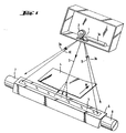
- the known system shown in Fig. 1 for checking a material web 4 by means of transmitted light comprises a laser source 1 a, from which a laser beam 1 is thrown onto a rotating mirror wheel 2, from which a reflected beam 3 emanates, which is one of the most deflected beam paths 3a and 3b passes over the limited area, its point of impact on its path from 3a to 3b also crossing the path 4 perpendicular to the direction of movement indicated by the arrow W.
- the beam 3 is modified by the web 4 and partially let through, and falls into the window 5 of the receiver 6, which is equipped with the photocells 7 and 8.
- the beam paths 10 and 11 illustrate areas in which the scanning beam does not strike the web during its scanning movement, but in which it reaches the window 5 of the receiver 6 directly.
- FIG. 2 shows, in the same embodiment of the device of the known type shown in FIG. 1, a polarizing strip 109 which is inserted between the web 4 and the opening of the window 5 of the receiver 6.
- the plane of the polarizer strip 109 is inclined at an acute angle with respect to the scanning plane as shown.
- the polarizer strip 109 is arranged so as to protrude over the longitudinal edges of the web on both sides next to the web 4 and is oriented such that it attenuates the light reflecting from it.
- preferred polarization directions 112 are indicated by arrows in the polarizer strip 109 shown in FIG.
- the beam is shown in this figure in the normal direction to the window 5 in the absence of the web 4.
- the polarization direction 113 of the beam 3 is selected such that it forms a small angle 0 with the axis a-a parallel to the edge L-M of the window 5.
- the polarization direction 113 forms an angle (90-0) with the axis b-b parallel to the edge M-N of the window 5.
- 4a and 4b illustrate the effect of a mirror wheel, the mirror surfaces of which are slightly tarnished or fogged.
- FIG. 4 a shows how the beam 1 from the laser source is reflected by a slightly tarnished mirror surface of the mirror wheel 2, with a main beam 3 and a narrow beam cone, which is limited, for example, by the scattered beams 3f i and 3f 2 , axially symmetrical about the main beam 3 is formed around.
- This cone of rays is also referred to below as scattered light.
- 4b shows the profile P of the scattered light cone surrounding the main beam.
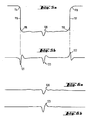
- 5a and 5b show to what extent the known system described above is unsuitable for checking web edge areas.
- a leading portion with scattered beam 3f falls on the web 4 and is partially damped by this before it reaches the receiver 6 through the window 5.
- the signal amplitude therefore begins to decrease, as indicated at 114.
- the main beam 3 now falls on path 4, causing the signal to drop sharply, as shown at 115.
- a trailing portion of the scattered light is additionally damped, which leads to a further, slower drop, as shown at 116.
- a similar abrupt change 117 with leading and trailing rounding effects 118 and 119 suffers the signal amplitude in the opposite sense as soon as the scanning beam 3 leaves the web 4, crossing the opposite web edge.
- the effect of a defect in the web or in its coating is indicated by the deflection 120 in FIG. 5a.
- the transients 121 and 122 caused by the abrupt changes 115 and 117 in the light amplitude together with the effects 114, 116, 118 and 119 are of the same order of magnitude as the transient 123 which is generated by the above-mentioned error location at 120 and are therefore without Appropriate signal suppression and the resulting loss of checking options in the vicinity of the web edges cannot be distinguished from the latter transient 123.
- 6a and 6b illustrate how, according to the present invention, the material web can be checked by means of transmitted light over the entire web surface.
- FIG. 6a shows how, with the aid of a polarizer strip 109 together with a correct polarization of the scanning beam 3, the signal can be influenced which is generated by the scanning beam 3 when the entire area between the beam paths 3a and 3b is scanned.
- the main beam 3 is completely polarized and the scattered light that occurs with it is also predominantly polarized along the same plane.
- each beam be it the main beam 3 or a beam of the scattered light cone surrounding it, is either passed through the polarizer strip 109 and polarized according to the value of 0, or it becomes polarized partially let through the path, where it polarizes arbitrarily on the polarizer strip 109 and then by one independent of 0 Amount is dampened.
- the resulting combined signal is therefore at the moment the beam crosses the edges
- the only remaining transient 120 is the one generated by a real flaw, so it is now possible to check the entire surface of the web 4.
- 6b shows the signal 123 after suitable filtering in order to distinguish abrupt changes from slow ones.
- FIG. 7 a shows how, by suitable choice of the angle of inclination of the polarizer strip 109, a portion of the light falling past the edge of the web 4 or scattered by the web near one of its two edges through the surface of the polarizer strip 109 to a second receiver or detector 124 can be reflected. The rest of the light is transmitted through the polarizer strip 109 in the manner already described.
- FIG. 7b schematically shows the same arrangement as FIG. 7a, but in a side view.
- FIG. 7c shows the response signal 125 generated by the auxiliary photo cell 124 when the scanning beam crosses a web edge.
- the steep change 126 in the course of the signal curve can be used for electronic switching purposes.
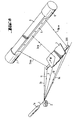
- a laser beam 1 is directed onto the rotating facets of a mirror wheel 2, from which the reflected beam is directed in such a way that it sweeps over a scanning path delimited by the boundary beams 3a and 3b and thereby also falls on the web 4.
- the point of incidence of the scanning beam 3 crosses the path in a direction perpendicular to the direction of travel W of the path.
- the beam 3 is modified and partially reflected by the path as beam 3 rw , which falls into the window 5 of the receiver containing the photocells 7 and 8.
- the beam 3 not only sweeps over the web 4 but also to the right and left of the same additional areas in which it remains unchanged on the reflection strip 209.
- Rays 10 and 11 are shown as individual rays in this edge region, for example, which are reflected along directions 10rm and 11rm, respectively, and which fall into the same window 5 of receiver 6.
- the figure shows in side view how a damping filter 212 in the path of deflected rays such. B. can be placed with 10rm and 11 rm.
- the density of the filter is chosen so that the average strength of the electrical signal generated by the photocells 7 and 8 due to the light reflected by the web is equal to the average strength of the deflected by the mirror 209 via the filter 212 to the receiver 6 Light generated signal is.
- the web runs over the two carrier rollers 213 and 214.
- FIGS. 4a and 4b show the effect of a slightly tarnished mirror surface of the mirror wheel, as a result of which a narrow beam cone is generated, the cladding of which is given by the two scattered light beams 3f 1 and 3f 2 .
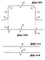
- Figures 10a and 10b show curves that illustrate that without the presence of the filter 212, the system would not be able to inspect the areas of the web extending along the web edges.
- 10a shows how the combined unfiltered signal generated in the photocells 7 and 8 changes while the scanning beam 3 scans the distance between the boundary beam paths 3a and 3b.
- 10b shows the curve shape of the signal after passing through a suitable high-pass filter. It can be seen from this that the transients 222 and 223 caused by the steep changes 216 and 218 and the rounding effects 215, 217, 219 and 220 are in the same order of magnitude as the transient 224 caused by a damaged area and therefore without suitable signal suppression and a corresponding loss cannot be distinguished from the transient 224 when checking the path over its entire surface.
- Figs. 1 1 and 11 b illustrate a web of material with incident light a review of the total web surface can be realized according to the invention as aspect of checking.
- a beam whether it is the main beam 3 or a beam of the scattered light cone, is either reflected by the web 4 so that it falls into the receiver 6 and thus its photocells 7 and 8 activated, or it is deflected by means of the mirror 209 and through the filter 212 into the same receiver and to its photocells.
- the signal caused by each such individual beam is therefore practically the same, regardless of whether the beam has hit the material web 4 or whether it has passed it laterally.
- the resulting combined signal is therefore essentially free of transients caused by crossing the web edges.
- the only remaining transient 221 is that caused by an actually existing fault location. It is therefore now possible to check the web 4 over its entire surface.
- 11 b shows the signal after a suitable high-pass filtering in order to distinguish between abrupt and slow changes.
- FIG. 12 shows a further embodiment of the device according to the invention.
- FIG. 13 shows how, in a further embodiment of the device according to the invention, the web 4 can be supported along the scanning path by a roller 229 which is polished to a high gloss.
- the light reflected by the web 4 is often scattered over a finite range of radiation directions, which is typically limited by the planes 230 and 231 indicated by lines in FIG. 13. Accordingly, the light is reflected on the polished roller 229 in the end regions of the scanning path along the plane 232.
- An adaptation of the average strengths of the signals caused on the one hand by the web and on the other hand by the roller can be achieved in such a way that a thin strip or a plate 233 made of filter material of suitable optical density is arranged in the plane 232.
- FIG. 14a and 14b show a further embodiment of the system according to the invention, which is equipped with a web edge detector.
- a beam splitter 234 is in the deflected by the light paths rays such. B. 10rm and 11rm level formed. This beam splitter 234 deflects a portion of the redirected light so that it, such as. B. is the case with beam 236, incident in an auxiliary photo cell 235.
- FIG. 14 b shows the course of the response signal 237, which is generated by the auxiliary photo cell 235 when crossing a web edge by the scanning beam 3.
- the steep amplitude change 238 can be used for electronic switching purposes.
- FIG. 15 A further embodiment of the device according to the invention is shown in FIG. 15, in which the light is focused into a photocell 242 with the aid of a lens.
- the beam 1 from a laser source is projected onto a rotating mirror wheel 2, from which it is reflected and, after further reflection at a mirror 239, is caused to sweep over a scanning distance delimited by the end points at 3a and 3b, the scanning beam 3 being directed onto the path 4 and strikes the reflective strips 209 on both sides of the web edges past the web.
- the scanning beam 3 which crosses the path 4 between the beam paths 3e 1 and 3e2 is reflected by the path and forms a reflection beam 3rw which sweeps over an area located between the boundary beam paths 3e i rw and 3e 2 rw on the flat front side of the focusing lens 243 and through the lens is concentrated in a focal point 240 near the window 241 of a photocell 242, whereupon it falls into the input window 241.
- Rays such as B. 10 rm and 11 rm in the path-free areas located between the web edges and the boundary beam paths 3a and 3b hit and are reflected by the mirror 209 are similarly concentrated by the focusing lens 243 at the focal point 244 and then likewise fall into that Input window 241 of the photocell 242.
- the adaptation of the rays to one another by reflection on the web 4 on the one hand and by reflection on the reflection strip 209 on the other hand is achieved by interposing a gray wedge 245 in the focal point 244, the gray wedge 245 but not intercepting rays focused in the focal point 240 may. Furthermore, a beam splitter 234 is inserted into the beam path immediately in front of the gray wedge 245 in order to direct a portion of the light reflected by the mirror 209 onto the auxiliary photo cell 235.
- the scanning beam 10 passing the web falls directly on a first auxiliary photocell 246 arranged next to and below the web 4, before it crosses the edge of the web 4 first encountered in the direction of sweep when it covers the route 3a-3b. Accordingly, after it has left the web 4, crossing its opposite edge, the scanning beam 11 falls on a second auxiliary photocell 247 arranged next to the other web edge.
- 16b schematically shows how signals from the photocells 7 and 8 caused by light rays 3rw reflected by the web 4 are added in an adder 248 and then amplified in the amplifier 249. Similarly, signals from auxiliary photocells 246 and 247 caused by light beams 10 and 11 are added in an adder 250 and then amplified in a control amplifier 251.
- the control amplifier 251 is set so that the amplitude of its output signal becomes equal to that of the amplifier 249.
- each beam regardless of whether it is the main beam 3 itself or a beam within the scattered light cone, is either reflected by the web 4 so that it is reflected in the receiver 6 falls and thus reaches the photocells 7 or 8, or it falls directly on the photocell 246 or 247.
- the signal caused by each such individual beam at the output of the adder 252 is practically always the same, regardless of whether the beam is from the Or not, and the only remaining transients in the signal obtained therefrom after filtering are those generated by real defective spots. Again, this makes it possible to inspect the entire surface of the web 4.
- the signal from the amplifier 251 can also be used for electronic switching purposes, for example.
- the method according to the invention minimizes abrupt changes in the electronic signals generated in the measuring unit when crossing the web edges by the scanning beam. The occurrence of stray light is also reduced.
Landscapes
- Engineering & Computer Science (AREA)
- Textile Engineering (AREA)
- Physics & Mathematics (AREA)
- Health & Medical Sciences (AREA)
- Life Sciences & Earth Sciences (AREA)
- Chemical & Material Sciences (AREA)
- Analytical Chemistry (AREA)
- Biochemistry (AREA)
- General Health & Medical Sciences (AREA)
- General Physics & Mathematics (AREA)
- Immunology (AREA)
- Pathology (AREA)
- Investigating Materials By The Use Of Optical Means Adapted For Particular Applications (AREA)
- Length Measuring Devices By Optical Means (AREA)
Claims (22)
Applications Claiming Priority (8)
| Application Number | Priority Date | Filing Date | Title |
|---|---|---|---|
| GB8118575 | 1981-06-17 | ||
| GB8118576 | 1981-06-17 | ||
| GB8118576 | 1981-06-17 | ||
| GB8118575 | 1981-06-17 | ||
| GB8129538 | 1981-09-30 | ||
| GB8129538 | 1981-09-30 | ||
| GB8135928 | 1981-11-27 | ||
| GB8135928 | 1981-11-27 |
Publications (2)
| Publication Number | Publication Date |
|---|---|
| EP0069061A1 EP0069061A1 (fr) | 1983-01-05 |
| EP0069061B1 true EP0069061B1 (fr) | 1985-01-23 |
Family
ID=27449252
Family Applications (1)
| Application Number | Title | Priority Date | Filing Date |
|---|---|---|---|
| EP82810250A Expired EP0069061B1 (fr) | 1981-06-17 | 1982-06-11 | Procédé et dispositif pour l'injection de bandes de matériel |
Country Status (3)
| Country | Link |
|---|---|
| US (1) | US4522497A (fr) |
| EP (1) | EP0069061B1 (fr) |
| DE (1) | DE3262033D1 (fr) |
Families Citing this family (18)
| Publication number | Priority date | Publication date | Assignee | Title |
|---|---|---|---|---|
| EP0130797B1 (fr) * | 1983-07-04 | 1989-04-19 | Konica Corporation | Méthode pour l'inspection de la surface d'un papier photographique |
| JPS60205337A (ja) * | 1984-03-30 | 1985-10-16 | Eisai Co Ltd | 不良アンプル剤を検出する方法及び装置 |
| JPS6175237A (ja) * | 1984-09-20 | 1986-04-17 | Nippon Soken Inc | 塗装面測定装置 |
| GB8424084D0 (en) * | 1984-09-24 | 1984-10-31 | Sira Ltd | Inspection apparatus |
| JPS61221063A (ja) * | 1985-03-25 | 1986-10-01 | Kanai Gakuen | 整列糸の糸切れ探知方法,および同方法に用いるフイ−ラ |
| DE3629004A1 (de) * | 1986-08-27 | 1988-03-10 | Agie Ag Ind Elektronik | Stromzufuehrung fuer eine drahtelektrode einer elektroerosionsmaschine |
| ES2033268T3 (es) * | 1987-08-18 | 1993-03-16 | Krauss U. Reichert Gmbh + Co. Kg Spezialmaschinenfabrik | Procedimiento y dispositivo para detectar y registrar defectos en piezas continuas de tejido. |
| JP2571245B2 (ja) * | 1987-12-29 | 1997-01-16 | ホーヤ株式会社 | 表面検査装置 |
| US4857747A (en) * | 1988-02-24 | 1989-08-15 | Albany International Corporation | Method and apparatus for analyzing the formation of a web of material via generating a formation index |
| JPH0641923B2 (ja) * | 1988-09-20 | 1994-06-01 | 株式会社東芝 | 表面検査装置 |
| JP3044713B2 (ja) * | 1989-01-12 | 2000-05-22 | 株式会社小森コーポレーション | 印刷物の品質検査装置及びその方 |
| EP0379281A3 (fr) * | 1989-01-19 | 1991-03-20 | Cosmopolitan Textile Company Limited | Méthode et appareil d'inspection d'une bande |
| JPH06207910A (ja) * | 1993-01-11 | 1994-07-26 | Fuji Photo Film Co Ltd | 表面検査装置 |
| US5867261A (en) * | 1997-04-28 | 1999-02-02 | International Business Machines Corporation | Surface inspection tool |
| DE10254880B4 (de) * | 2001-12-14 | 2009-06-10 | Heidelberger Druckmaschinen Ag | Verfahren zum Erkennen von Kanten von blattförmigen Materialien |
| US20050041251A1 (en) * | 2003-08-18 | 2005-02-24 | Hong Cao | Method and apparatus for measuring loading of waterproofing agent in carbon substrate |
| US8812149B2 (en) | 2011-02-24 | 2014-08-19 | Mss, Inc. | Sequential scanning of multiple wavelengths |
| US8524442B1 (en) | 2012-02-13 | 2013-09-03 | David A. Recchia | Integrated membrane lamination and UV exposure system and method of the same |
Family Cites Families (11)
| Publication number | Priority date | Publication date | Assignee | Title |
|---|---|---|---|---|
| DE1296822B (de) * | 1959-12-22 | 1969-06-04 | Feldmuehle Ag | Vorrichtung zur laufenden UEberwachung von Papier, Pappe, Folien oder sonstigen bahn- oder blattfoermigen Erzeugnissen auf optisch erkennbare Abweichungen (Fehlerstellen) |
| DE1125679B (de) * | 1960-10-14 | 1962-03-15 | Philips Nv | Vorrichtung zur Anzeige von Flecken auf einer Oberflaeche |
| DE1573641C3 (de) * | 1965-05-08 | 1974-01-03 | Paul 5450 Neuwied Lippke | Vorrichtung zur Verbesserung des Verhältnisses zwischen den Störsignalen und dem Nutzsignal bei der elektronischoptischen, auf Lichtreflexion beruhenden Prüfung von Papieren |
| DE1573900A1 (de) * | 1966-11-07 | 1970-09-03 | Walter Neubert | Pruefgeraet zum Pruefen fehlerhafter Folien |
| DE2043876A1 (de) * | 1970-09-04 | 1972-03-09 | Licentia Gmbh | Anordnung zur Erfassung von Fehlern in durchsichtigen Bahnen |
| GB1366369A (en) * | 1971-11-30 | 1974-09-11 | Ferranti Ltd | Detection of faults on surfaces |
| US3826578A (en) * | 1972-12-08 | 1974-07-30 | Laser Sciences Inc | Scanning inspection system and method |
| US3843890A (en) * | 1973-07-27 | 1974-10-22 | Du Pont | Optical-electrical web inspection system |
| CH608628A5 (fr) * | 1975-11-21 | 1979-01-15 | Sick Optik Elektronik Erwin | |
| GB2018985B (en) * | 1978-02-13 | 1983-01-06 | Sira Institute | Detecting flaws in sheets |
| US4422766A (en) * | 1981-07-27 | 1983-12-27 | Ppg Industries, Inc. | Method of and device for reducing apparatus response time during the testing for moisture content in moving spaced plastic sheets |
-
1982
- 1982-06-07 US US06/385,593 patent/US4522497A/en not_active Expired - Fee Related
- 1982-06-11 EP EP82810250A patent/EP0069061B1/fr not_active Expired
- 1982-06-11 DE DE8282810250T patent/DE3262033D1/de not_active Expired
Also Published As
| Publication number | Publication date |
|---|---|
| EP0069061A1 (fr) | 1983-01-05 |
| DE3262033D1 (en) | 1985-03-07 |
| US4522497A (en) | 1985-06-11 |
Similar Documents
| Publication | Publication Date | Title |
|---|---|---|
| EP0069061B1 (fr) | Procédé et dispositif pour l'injection de bandes de matériel | |
| DE3309584C2 (fr) | ||
| DE19960653B4 (de) | Verfahren und Vorrichtung für die Detektion oder Lagebestimmung von Kanten | |
| DE3728210C2 (fr) | ||
| DE69307322T2 (de) | Vorrichtung zur erfassung von fehlern in fasermaterialien | |
| DE2827704C3 (de) | Optische Vorrichtung zur Bestimmung der Lichtaustrittswinkel | |
| DE2256736A1 (de) | Verfahren zur automatischen oberflaechenprofilmessung und vorrichtung zur durchfuehrung des verfahrens | |
| DE2152510A1 (de) | Verfahren zum Nachweisen von Oberflaechenfehlern | |
| DE2802286C2 (fr) | ||
| EP0123929A2 (fr) | Dispositif pour la détection de défauts | |
| DE3446355A1 (de) | Optisches fehlersuchgeraet | |
| DE3507139C2 (fr) | ||
| DE4007401A1 (de) | Messvorrichtung | |
| DE2532603B2 (de) | Optische Vorrichtung zur Bestimmung des Lichtaustrittswinkels | |
| DE2344579A1 (de) | Vorrichtung zum auffinden von fehlern in flaechen oder bahnen | |
| DE69421649T2 (de) | Optische Prüfvorrichtung für die Füllung von Zigaretten | |
| EP0218865B1 (fr) | Dispositif pour la détection sans contact de défauts dans des surfaces non structurées | |
| EP0331272B1 (fr) | Procédé et dispositif pour l'inspection de bandes transparentes | |
| DE2718711C2 (fr) | ||
| DE3017672A1 (de) | Vorrichtung und verfahren zum nachweis von loechern in platten-, blatt- oder folienmaterial | |
| DE3786888T2 (de) | Detektor zum Abtasten der Grösse eines Dokuments für ein Kopiergerät. | |
| DE2827705B2 (de) | Gerät zur Feststellung von Fehlern an Bahnmaterial | |
| EP1122536A2 (fr) | Méthode et dispositif pour détecter optiquement des déformations locales d'un support de données optiques, notamment des bulles | |
| DE2518828A1 (de) | Lichtschranke | |
| DE4006618C2 (de) | Vorrichtung zur Auskoppelung einer Meßstrahlung aus einem Laserstrahl |
Legal Events
| Date | Code | Title | Description |
|---|---|---|---|
| PUAI | Public reference made under article 153(3) epc to a published international application that has entered the european phase |
Free format text: ORIGINAL CODE: 0009012 |
|
| 17P | Request for examination filed |
Effective date: 19820614 |
|
| AK | Designated contracting states |
Designated state(s): BE CH DE FR GB IT LI |
|
| ITF | It: translation for a ep patent filed | ||
| GRAA | (expected) grant |
Free format text: ORIGINAL CODE: 0009210 |
|
| AK | Designated contracting states |
Designated state(s): BE CH DE FR GB IT LI |
|
| REF | Corresponds to: |
Ref document number: 3262033 Country of ref document: DE Date of ref document: 19850307 |
|
| ET | Fr: translation filed | ||
| PLBE | No opposition filed within time limit |
Free format text: ORIGINAL CODE: 0009261 |
|
| STAA | Information on the status of an ep patent application or granted ep patent |
Free format text: STATUS: NO OPPOSITION FILED WITHIN TIME LIMIT |
|
| 26N | No opposition filed | ||
| PGFP | Annual fee paid to national office [announced via postgrant information from national office to epo] |
Ref country code: FR Payment date: 19890414 Year of fee payment: 8 |
|
| PGFP | Annual fee paid to national office [announced via postgrant information from national office to epo] |
Ref country code: GB Payment date: 19890430 Year of fee payment: 8 |
|
| PGFP | Annual fee paid to national office [announced via postgrant information from national office to epo] |
Ref country code: DE Payment date: 19890510 Year of fee payment: 8 |
|
| PGFP | Annual fee paid to national office [announced via postgrant information from national office to epo] |
Ref country code: CH Payment date: 19890620 Year of fee payment: 8 |
|
| PGFP | Annual fee paid to national office [announced via postgrant information from national office to epo] |
Ref country code: BE Payment date: 19890622 Year of fee payment: 8 |
|
| ITTA | It: last paid annual fee | ||
| PG25 | Lapsed in a contracting state [announced via postgrant information from national office to epo] |
Ref country code: GB Effective date: 19900611 |
|
| PG25 | Lapsed in a contracting state [announced via postgrant information from national office to epo] |
Ref country code: LI Effective date: 19900630 Ref country code: CH Effective date: 19900630 Ref country code: BE Effective date: 19900630 |
|
| BERE | Be: lapsed |
Owner name: CIBA-GEIGY A.G. Effective date: 19900630 |
|
| GBPC | Gb: european patent ceased through non-payment of renewal fee | ||
| PG25 | Lapsed in a contracting state [announced via postgrant information from national office to epo] |
Ref country code: FR Effective date: 19910228 |
|
| REG | Reference to a national code |
Ref country code: CH Ref legal event code: PL |
|
| PG25 | Lapsed in a contracting state [announced via postgrant information from national office to epo] |
Ref country code: DE Effective date: 19910301 |
|
| REG | Reference to a national code |
Ref country code: FR Ref legal event code: ST |